EP0639760B1 - Halbleiter für Differentialdruck-Messapparat und Verfahren zu seiner Herstellung - Google Patents
Halbleiter für Differentialdruck-Messapparat und Verfahren zu seiner Herstellung Download PDFInfo
- Publication number
- EP0639760B1 EP0639760B1 EP93113215A EP93113215A EP0639760B1 EP 0639760 B1 EP0639760 B1 EP 0639760B1 EP 93113215 A EP93113215 A EP 93113215A EP 93113215 A EP93113215 A EP 93113215A EP 0639760 B1 EP0639760 B1 EP 0639760B1
- Authority
- EP
- European Patent Office
- Prior art keywords
- diaphragm
- etching
- silicon
- concave portion
- differential pressure
- Prior art date
- Legal status (The legal status is an assumption and is not a legal conclusion. Google has not performed a legal analysis and makes no representation as to the accuracy of the status listed.)
- Expired - Lifetime
Links
Images







Classifications
-
- G—PHYSICS
- G01—MEASURING; TESTING
- G01L—MEASURING FORCE, STRESS, TORQUE, WORK, MECHANICAL POWER, MECHANICAL EFFICIENCY, OR FLUID PRESSURE
- G01L19/00—Details of, or accessories for, apparatus for measuring steady or quasi-steady pressure of a fluent medium insofar as such details or accessories are not special to particular types of pressure gauges
- G01L19/06—Means for preventing overload or deleterious influence of the measured medium on the measuring device or vice versa
- G01L19/0618—Overload protection
-
- G—PHYSICS
- G01—MEASURING; TESTING
- G01L—MEASURING FORCE, STRESS, TORQUE, WORK, MECHANICAL POWER, MECHANICAL EFFICIENCY, OR FLUID PRESSURE
- G01L19/00—Details of, or accessories for, apparatus for measuring steady or quasi-steady pressure of a fluent medium insofar as such details or accessories are not special to particular types of pressure gauges
- G01L19/06—Means for preventing overload or deleterious influence of the measured medium on the measuring device or vice versa
- G01L19/0627—Protection against aggressive medium in general
- G01L19/0636—Protection against aggressive medium in general using particle filters
-
- G—PHYSICS
- G01—MEASURING; TESTING
- G01L—MEASURING FORCE, STRESS, TORQUE, WORK, MECHANICAL POWER, MECHANICAL EFFICIENCY, OR FLUID PRESSURE
- G01L9/00—Measuring steady of quasi-steady pressure of fluid or fluent solid material by electric or magnetic pressure-sensitive elements; Transmitting or indicating the displacement of mechanical pressure-sensitive elements, used to measure the steady or quasi-steady pressure of a fluid or fluent solid material, by electric or magnetic means
- G01L9/0041—Transmitting or indicating the displacement of flexible diaphragms
- G01L9/0042—Constructional details associated with semiconductive diaphragm sensors, e.g. etching, or constructional details of non-semiconductive diaphragms
-
- G—PHYSICS
- G01—MEASURING; TESTING
- G01L—MEASURING FORCE, STRESS, TORQUE, WORK, MECHANICAL POWER, MECHANICAL EFFICIENCY, OR FLUID PRESSURE
- G01L9/00—Measuring steady of quasi-steady pressure of fluid or fluent solid material by electric or magnetic pressure-sensitive elements; Transmitting or indicating the displacement of mechanical pressure-sensitive elements, used to measure the steady or quasi-steady pressure of a fluid or fluent solid material, by electric or magnetic means
- G01L9/0041—Transmitting or indicating the displacement of flexible diaphragms
- G01L9/0051—Transmitting or indicating the displacement of flexible diaphragms using variations in ohmic resistance
- G01L9/0052—Transmitting or indicating the displacement of flexible diaphragms using variations in ohmic resistance of piezoresistive elements
- G01L9/0055—Transmitting or indicating the displacement of flexible diaphragms using variations in ohmic resistance of piezoresistive elements bonded on a diaphragm
Definitions
- the present invention relates to a compact and low cost differential pressure measurement apparatus having a simple structure and yet elaborate, which can manufactured without any special pressure resistant casing or any protective mechanism against overpressure, and free of pressure-resistant hermetic terminals.
- the present invention also relates to a semiconductor type differential pressure measurement apparatus comprising a measuring diaphragm provided on both sides thereof with two measuring chambers each having a predetermined spacing such that they may be immediately backed by the wall of the measuring chamber when an over pressure is applied to the measuring diaphragm; it directly utilizes the strain detector for measuring the pressure difference as the detector element for overpressure, and therefore is a simple and inexpensive semiconductor type differential pressure measurement apparatus yet highly reliable for detecting overpressure.
- the present invention further relates to a semiconductor type differential pressure measurement apparatus manufacturing method which is inexpensive and can manufacture diaphragms with highly precise thicknesses.
- the present invention also relates to a method for manufacturing a semiconductor type differential pressure measure apparatus by sacrificial layer etching method whereby there is no possibility diaphragm to the substrate.
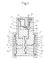
- FIG. 1 is an explanatory drawing of a prior art structure. Reference may be made, for example, to FIG. 1 of JP-A-59-56137 (the term "JP-A-" as referred to herein signifies "a published unexamined Japanese patent application").
- a flange 2 and another flange 3 are fitted and assembled on both sides of a housing 1 by means of welding or the like, and an inlet 5 for introducing a high pressure fluid with a pressure of P H and an inlet 4 for a low pressure fluid with a pressure of P L are provided on both of the flanges 2 and 3.
- a pressure measuring chamber 6 equipped with a center diaphragm 7 and a silicon diaphragm 8 is established inside the housing 1.
- the center diaphragm 7 and the silicon diaphragm 8 are each separately fixed on the wall of the pressure measuring chamber 6 to divide the chamber 6 into two parts.
- Back plates 6A and 6B are provided on the wall of the pressure measuring chamber 6 in such a manner that they face the center diaphragm 7.
- the periphery of the center diaphragm is welded to the housing 1.
- the silicon diaphragm 8 is made entirely from a single crystal substrate.
- strain gauges 80 are formed on one side of a silicon substrate by selective diffusion of an impurity such as boron, and the other side is subjected to machining and etching to form a concave diaphragm.
- an impurity such as boron
- the strain gauges are connected to a Wheatstone bridge to detect the change of differential pressure ⁇ P as a change in electric resistance.
- a lead 81 is attached at one end to the strain gauge 80, and is connected to a hermetic terminal 82 at the other end.
- the hermetic terminal is held by a support 9.
- the end of the support 9 facing the pressure measuring chamber 6 is fixed and adhered to the silicon diaphragm 8 using a low melting point glass or the like.
- Pressure-introducing chambers 10 and 11 are provided between the housing 1 and each of the flanges 1 and 2.
- Liquid separation diaphragms 12 and 13 are further provided inside the pressure-introducing chambers 10 and 11, and back plates 10A and 11A having shapes similar to the liquid separation diaphragms 12 and 13 are formed on the wall of the housing 1 in such a manner that they face the liquid separation diaphragms 12 and 13.
- the liquid separation diaphragms 12 and 13 together with the back plates 10A and 11A define a space communicating with the pressure measuring chamber 6 via communicating holes 14 and 15.
- Portions 101 and 102 filled with a sealed liquid such as silicon oil are provided between the liquid separation diaphragms 12 and 13 in such a manner that the sealed liquid may reach the upper and the lower planes of the silicon diaphragm through the communicating holes 16 and 17.
- the sealed liquid is separated into the portions 101 and 102 by the center diaphragm 7 and the silicon diaphragm 8 such that the amounts in both are substantially equal.
- the aforementioned construction allows transmission of a pressure being exerted from the high pressure side, by transmitting the pressure applied to the liquid separation diaphragm 13, to the silicon diaphragm 8 via the sealed liquid portion 102.
- a pressure is applied from the low pressure side, on the other hand, the pressure exerted to the liquid separation diaphragm 12 is transmitted to the silicon diaphragm 8 via the sealed liquid portion 101.
- the silicon diaphragm 8 is deformed by the pressure difference between the pressure on the high pressure side and that on the low pressure side.
- This quantity of deformation i.e., strain
- the strain gauge 80 for measuring differential pressure.
- Such an overpressure protection means is disclosed e.g. in EP-A-0 490 486, providing a differential pressure transducer formed on semiconductor substrates.
- the substrates include a membran being mounted to and sealed to the substrate at the peripheral edges of the membran.
- the bottom of the cavity forms an overpressure stop to prevent overdeflections of the membran towards the substrate.
- An overpressure stop formed as a bridge extends above the membran and is spaced therefrom to allow the membran to deflect freely under normal pressure situations but prevent overdeflections.
- the present invention provides means for overcoming the aforementioned problems.
- An object of the present invention is to provide, economically, a high performance compact differential pressure measuring apparatus free from any special pressure resistant casing or a separate protective mechanism against over pressure, yet without using any pressure resistant hermetically sealed terminals.
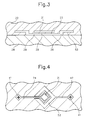
- FIG. 2 is an explanatory figure of the essential portion of an embodiment according to the present invention.
- FIG. 3 shows a cross sectional view taken along line A-A of FIG. 2
- FIG. 4 is a cross sectional view taken along line B-B of FIG. 2.
- a first chamber 21 having an extremely narrow predetermined spacing is provided on a silicon substrate 22 to form a diaphragm 23.
- a first communicating hole 24 which communicates with the first chamber 21 at one of its ends is established on a silicon substrate 22, and a thin film concave portion 25 is provided in the diaphragm 23 on the side opposite to the face on which the first chamber 21 is provided.
- a second chamber 26 communicating with the concave portion 25 is provided on the silicon substrate 22, and the diaphragm 23 is surrounded by this second chamber in a ring-like manner except at the first communicating hole 24.
- a strain detector element 27 is provided on the side of the diaphragm 23 facing the concave portion 25.
- a support substrate 28 is joined by one surface thereof with the surface of the silicon substrate 22 on which the concave portion is provided, and it, together with the concave portion 25, defines a chamber 29 and the second chamber 26.
- connection 31 is formed by introducing impurities into the joint surface between the silicon substrate 22 and the support substrate 28, and is connected to the strain detector element 27 at one end.
- a contact 32 is provided to support substrate 28 on the joint side with the silicon substrate 22, and is connected to the connection 31 at one end.
- a groove 33 is formed on the silicon substrate 22 at the vicinity of the contact 32.
- the groove 33 imparts an appropriate repulsive force to the contact portion between the silicon substrate 22 and the contact 32 to assure stable contact between the contact 32 and the connection 31.
- a filter portion 41 is provided to the silicon substrate 22 to prevent the inclusions contained in the fluid, i.e., the pressure medium, from entering the first chamber 21 or the chamber 29.
- two filter portions are established in the structure.
- the inclusion of unfavorable dust or particles is avoided by applying a semiconductor fabrication process to provide a sufficiently small gap d for the filter portion 41. That is, the gap d of the filter portion 41 is formed in such a manner that it may be sufficiently small as to satisfy the relation d ⁇ (A - B), wherein A represents the spacing of the first chamber 21, and B represents the displacement of the diaphragm 23.
- One side of the filter portion 41 is connected to the first communicating hole 24, and the other side is connected to the chamber 29 via the second communicating hole 42.
- a first connection hole 51 for introducing pressure is established on the supporting substrate 28 and connected to one of the sides of the filter portion 41. The other end of this hole 51 is left open to the atmosphere.
- a second connection hole 52 for introducing pressure is established on the supporting substrate 28 and connected to one of the sides of the filter portion 41. The other end of this hole 52 is left open to the atmosphere.
- An extending portion, or overhang, 53 is connected to the second chamber 26.
- the overhang 53 is provided such that it may receive a high pressure in case such a high pressure is applied to the overhang 53, thereby preventing great stress from generating at the joint portion between the silicon substrate 22 and the support substrate 28.
- the measuring pressure of the high pressure side is applied to the first chamber 21 whereas that of the low pressure side is applied to the chamber 29.
- the silicon diaphragm 23 is deformed in accordance with the pressure difference between the higher and lower pressure sides, and the strain thus generated is electrically detected by the strain detector element 27.
- differential pressure can be measured by drawing out the strain externally as an electrical signal via a lead 31 and a contact 32.
- a desired pattern 102 is etched out on an SOI (silicon on insulator) wafer 101 by RIE (reactive ion enhanced) etching a silicon oxide layer 103 and a silicon layer 104.
- RIE reactive ion enhanced
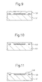
- An epitaxially grown layer 105 is established on the surface of the SOI wafer 101 as shown in FIG. 9.
- the surface of the epitaxially grown layer 105 is polished as in FIG. 10 to obtain a mirror surface.
- the surface of the epitaxially grown layer 105 is etched by RIE etching to form a concave portion 106.
- a hole 107 for etching the buried silicon oxide layer 103 is formed by either RIE etching or wet etching using potassium hydroxide.
- the surface of the silicon oxide layer 103 is etched using an aqueous hydrogen fluoride solution or a hydrogen fluoride gas, as illustrated in FIG. 13.
- a silicon substrate 22 is anodically joined to a support substrate 28 made from Pyrex glass.
- the resulting structure is shown in FIG. 14.
- the present invention economically provides, a high performance compact differential pressure measurement apparatus free from any special pressure resistant casing or a separate protective mechanism against overpressure, yet without using any pressure resistant hermetically sealed terminals.
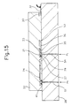
- FIG. 15 is an explanatory figure showing the essential portion of an apparatus according to another embodiment of the present invention.
- the apparatus according to the present embodiment is characterized in that a third connection hole 54 for introducing pressure and communicating directly to a chamber 29 is provided on a support substrate 28.
- the support substrate 28 may be made of silicon or polysilicon (polycrystalline silicon) instead of Pyrex.
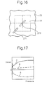
- strain detector elements 271 and 272 are arranged generally on the diaphragm 23 in such a manner that maximum sensitivity is achieved. More specifically, one element is placed at the center and the other on the edge of the diaphragm 23, so that they may undergo reverse phase operation.
- the differential pressure measurement apparatus shown in FIG. 2 receives overpressure directly with the diaphragm 23. Accordingly, the measuring diaphragm 23 displaces and, if it surpasses the predetermined spacing, immediately backs onto the wall of the first chamber 21 or the chamber 29 which both function as a measuring chamber.
- the relationship between the strain detected by the strain detector elements 271 and 272 and the applied pressure is shown in FIG. 17.
- the curves indicated by A and B in the graph are strain curves obtained by the detector elements 271 and 272, respectively, and the curve indicated by C corresponds to the difference between the strain obtained by the detector elements 271 and 272.
- a tensile strain can be detected when an overpressure is applied from the direction indicated with an arrow marked D until the diaphragm 23 touches the wall of the first chamber 21.
- the detected strain ⁇ cannot be definitely designated an overpressure, because the strain as read may be identified as either a pressure P1 within the allowable measurement range or a pressure P2 belonging to the overpressure range.
- the detector element 271 is subject to various changes in conditions with respect to, for example, static pressure and temperature.
- a static pressure is applied in addition to differential pressure, for instance, the strain detected by the strain detector element 271 includes an additional offset. Accordingly, the true characteristic curve for the strain indicated by E in the graph of FIG. 23 may be displaced to give curve F as shown in the same graph. If the initial strain under overpressure should be determined as ⁇ , the actual overpressure may slip from P3 to P4 making detection thereof impossible.
- the difference between the output signals from the strain detector elements 271 and 272 may be calculated and used for judging the overpressure.
- FIG. 25 is given the relation between the applied overpressure and the strain detected by the strain detector element 272 (the curve marked with G) and that between the applied pressure and the strain detected by the strain detector element 271 (the curve marked with H).
- a means of providing a detector element for detecting overpressure in addition to the strain detector elements 271 and 272 can be considered.
- the installation of an additional strain detector element for detecting overpressure requires novel structures and electric circuits to be incorporated. This inevitably causes an increase in the manufacturing cost and additional process steps to be incorporated in the manufacturing method.
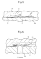
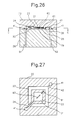
- FIG. 26 is shown an explanatory figure of the essential portion of another embodiment according to the present invention.
- FIG. 27 shows a cross sectional view taken along line C-C of FIG. 26.
- a first strain detector element 61 is placed at the edge portion of the measuring diaphragm 23.
- a second strain detector element 62 is placed at a position slightly offset from the center of the diaphragm 23 in such a manner that the differential between the output signal therefrom and that from the first strain detector element 61 may change as a single-value function (i.e., the differential signal is in one-to-one correspondence with the applied pressure).
- a means 63 for detecting overpressure which detects the differential signal between the signals from the first strain detector element 61 and the second strain detector element 62 is provided to judge whether an overpressure is applied or not.
- the means 63 for detecting overpressure may comprise a CPU (central processing unit) 65 to perform differential calculation on the signals from the first strain detector element 61 and the second strain detector element 62, and a signal based on the judgement after comparing the differential with the standard signal 67 using a comparator is output as an overpressure judging signal 68.
- a detection signal 71 for the differential of measured pressure is also output from the results obtained through the calculation in the CPU 65.
- a measuring pressure of the high pressure side and a measuring pressure of the low pressure side are applied respectively to the measuring chambers 21 and 29 provided on both sides of the measuring diaphragm 23. Then, as a result, the silicon diaphragm 23 deforms in correspondence to the pressure difference between the applied higher and lower pressures.
- the strain resulting from the deformation of the diaphragm is electrically detected by the strain detector elements 61 and 62, and the signal corresponding to the strain is output to the exterior via a lead 31 and a contact 32 to give the differential pressure.
- FIG. 30 is given the relation between the applied overpressure and the strain detected by the strain detector element 61 (the curve marked with I) and that between the applied pressure and the strain detected by the strain detector element 62 (the curve marked with J).
- the graph shown in FIG. 31 shows the relation between the overpressure and the difference between the strain detected by the detector elements 61 and 62.
- the signal for the difference in strain yields a characteristic curve exhibiting an abrupt decrease from the point where the diaphragm 23 contacts with the wall of the measuring chambers 21 and 29. Reference may be made to FIG. 24 for such a characteristic curve.
- that according to the present invention yields a uniformly increasing curve as shown in FIG. 31 for the differential of the detected strains. Since the strain can be expressed as a single-valued function of the applied pressure (i.e., the difference between the detected strains is in one-to-one correspondence to the applied pressure), whether an overpressure is applied or not can be easily judged.
- This advantage in the apparatus according to the present invention is believed to be attributable to the fact that decrease in the detected strain for the strain detector element 62 is somewhat relaxed as compared with the abrupt recovery of the strain in the conventional strain detector element 272. More specifically, it is believed that the strain recovery occurs only in a part of the fixed portions of the strain detector element 62 and that it does not take place at other fixed portions.
- a semiconductor type differential pressure measurement apparatus capable of detecting overpressure with high reliability.
- the overpressure can be detected with high reliability by using a semiconductor differential pressure measuring apparatus equipped with a measuring diaphragm 23 which can be readily backed up by the walls of chambers 21 and 29, provided that one of the strain detector elements, i.e., the element 62, is placed slightly offset from the center of the diaphragm 23, and thereby calculating the difference between the strain detected by the strain detector element 62 and the strain detector element 61 established on the edge portion of the diaphragm 23.
- the apparatus according to the present invention can be manufactured without a separate strain detector element for detecting overpressure. Accordingly, a simple and highly reliable semiconductor type differential pressure measurement apparatus can be economically obtained with good economy.
- the apparatus according to the present invention can be obtained by slightly displacing the position of the strain detector element from the position in a conventional apparatus. It follows that the apparatus according to the present invention can be fabricated by a slight change in the semiconductor fabrication process such as changing the etching pattern. Thus, the acquired knowledge in manufacturing semiconductors can be fully utilized to obtain good product yield.
- the present invention realizes a simple and economical semiconductor type differential pressure measurement apparatus which is capable of detecting overpressure with high reliability.
- the precision of finishing the diaphragm 23 to a desired thickness depends on the polishing step as shown in FIG. 10. Polishing methods in general yield a precision of about ⁇ 5 ⁇ m for a finished thickness of 500 ⁇ m, and a higher precision cannot be achieved.
- the thickness of the diaphragm used in the apparatus according to the present invention is about 20 ⁇ m. However, a dimensional precision of ⁇ 5 ⁇ m is too large and impairs the product yield. A poor product yield raises the manufacturing cost.
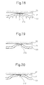
- FIGs. 32 to 41 another embodiment according to the present invention for overcoming the problem above is described below. More specifically, a method for manufacturing a semiconductor type differential pressure measurement apparatus as illustrated in FIG. 2 is explained. The present method provides an apparatus equipped with a diaphragm whose thickness dimension is controlled with high precision, and yet which is economical.
- an SOI wafer having a silicon oxide layer 203 and a silicon layer 204 is subjected to RIE etching to remove the predetermined portions 202.
- the silicon substrate 204 is about 600 ⁇ m in thickness, and comprises thereon the silicon oxide layer 203 which is about 1 ⁇ m thick and the silicon layer 204 which is about 0.5 ⁇ m thick.
- An epitaxially grown layer 205 is then grown to a thickness of about 20 ⁇ m on the surface of the SOI wafer 201.
- the resulting structure is shown in FIG. 33.
- the thickness of the diaphragm 23 depends on the thickness of this epitaxially grown layer 205.
- a silicon oxide film 206 is then patterned on the peripheral surface of the epitaxially grown layer 205. This structure is shown in FIG. 34.
- the thus patterned silicon oxide film 206 functions as a stopper in the selective polishing.
- an epitaxially grown layer 207 is developed at a predetermined thickness on the surface of the previously obtained epitaxially grown layer 205.
- the epitaxially grown layer 207 may be established, for instance, at a thickness of about 5 ⁇ m.
- the resulting structure is subjected to selective polishing using the silicon oxide film 206 as a stopper.
- This step is conducted by mechanical polishing using a polishing solution comprising a weakly alkaline solution having suspended therein colloidal silica (a fine powder of silicon oxide). Because the ratio of the polishing rate of silicon to that of silicon oxide amounts to about 100, polishing does not advance beyond the silicon oxide film 206.
- the silicon oxide film 206 is then removed by etching to give the structure shown in FIG. 37.
- a concave portion 208 is etched on the epitaxially grown layer 205 by RIE etching to give the structure shown in FIG. 38.
- a hole 208 for use in etching the silicon oxide layer 203 in the SOI wafer is perforated in the epitaxially grown layer 205 by etching, using either RIE etching or potassium hydroxide.
- the silicon oxide layer 203 is etched using either an aqueous hydrogen fluoride solution or a hydrogen fluoride gas.
- a silicon substrate 22 is anodically joined with a support substrate 28 made of Pyrex glass to obtain the structure shown in FIG. 41.
- the thus obtained structure readily results in a semiconductor type differential pressure measurement apparatus comprising a diaphragm 23 having a thickness controlled with high precision.
- a diaphragm with high dimensional precision was achieved by patterning a silicon oxide film 206 on the surface of the periphery of the epitaxially grown layer 205 and conducting thereafter selective polishing using the silicon oxide film 206 as the stopper.
- This method as a result, has a greatly reduced manufacturing cost.
- the diaphragm 23 was obtained at a thickness of 20 ⁇ m and with a precision as high as ⁇ 0.5 ⁇ m.
- the SOI substrate may be replaced by a silicon substrate obtained by forming thereon a patterned silicon oxide film and further thereon a polysilicon layer.
- the present invention provides a method for manufacturing a semiconductor type differential pressure measurement apparatus capable of economically realizing a diaphragm of high dimensional precision.
- a sacrificial layer etching technique may be applied in the establishment of the first chamber 21 between the diaphragm 23 and the silicon substrate 22.
- sacrificial layer etching refers to a method in which first a sacrificial layer is provided between a substrate and a structural layer (a layer which functions as a constituent of a structure), and finally the sacrificial layer alone is removed by selective etching to provide an opening between the structure and the substrate.
- a structural layer a layer which functions as a constituent of a structure
- the sacrificial layer alone is removed by selective etching to provide an opening between the structure and the substrate.
- the diaphragm 23 On drying the diaphragm 23 after rinsing, the diaphragm 23 tends to be adsorbed into the silicon substrate 22 by the surface tension of the rinsing solution, and it often occurs that the diaphragm cannot be easily separated from the silicon substrate 22.
- the surfaces of the diaphragm 23 and the silicon substrate 22 are rendered adhesive after the silicon oxide layer 103 is etched, because hydroxyl ion (OH - ) groups remain attached to the dangling bonds of the surface silicon atoms. Since those OH - groups readily combine with each other to generate H 2 O, the silicon atoms are thereby combined by oxygen atoms.
- FIGs. 42 to 49 another embodiment according to the present invention for overcoming the problem above is described below. More specifically, a method for manufacturing a semiconductor type differential pressure measurement apparatus free from mutual adhesion of the diaphragm 23 and the silicon substrate 22 is described below.
- FIG. 42 an SOI wafer having a silicon oxide layer 303 and then a silicon layer 304 is subjected to RIE etching to remove the predetermined portions 302.
- FIG. 43 gives a planar view of the structure shown in FIG. 42.
- An epitaxially grown layer 305 is then established on the surface of the SOI wafer 301.
- the resulting structure is shown in FIG. 44.
- the surface of the epitaxially grown layer 305 is subjected to polishing to obtain a mirror surface.
- the thus obtained epitaxially grown layer 305 is then subjected to RIE etching to give a concave portion 306.
- the resulting structure is shown in FIG. 46.
- a hole 307 for use in etching the buried silicon oxide layer 303 in the SOI wafer is perforated in the epitaxially grown layer 306 by etching, using either RIE etching or potassium hydroxide.
- the structure is subjected to vapor phase etching in a mixed gas comprising hydrogen fluoride gas and a trace amount of water vapor, using the silicon oxide layer 303 as the sacrificial layer.
- the vapor phase etching of the sacrificial layer may be conducted, for example, in a mixed gas containing 95% nitrogen gas, 4.99% hydrogen fluoride gas, and 0.01% water vapor.
- the mixing ratio of the gas components is given only as an example, and other gas mixtures may be used so long as vapor phase etching might be conducted therein.
- a silicon substrate 22 is anodically joined with a support substrate 28 made of Pyrex glass to obtain the structure shown in FIG. 49.
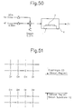
- FIG. 50 An etching apparatus according to the present invention is shown schematically in FIG. 50.
- the apparatus comprises a chamber K, a sample support L with a wafer M to be etched being mounted thereon.
- the vapor phase etching in this apparatus proceeds according to a reaction scheme expressed as follows: SiO 2 + HF + H 2 O ⁇ SiF 4 ⁇ + H 2 O ⁇ Nitrogen (N 2 ) gas is circulated at a sufficient amount to drive out gaseous silicon fluoride (SiF 4 ) and water (H 2 O) from the system and thereby prevent liquefaction from occurring.
- the diaphragm 23 and the silicon substrate 22 can be prevented from adhering to each other by the surface tension of the remaining liquid.
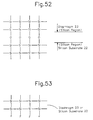
- a wet etching process produces silicon surfaces as illustrated in FIG. 51 upon etching of silicon oxide (SiO 2 ). It can be easily understood that the diaphragm 23 and the silicon substrate 22 readily combines with each other through a tight chemical bonding as shown schematically in FIG. 52.
- the etching of the silicon oxide sacrificial layer 303 using vapor phase etching not only avoids adhesion of the constituent members in the etching step, but also provides an inert surface after etching. Accordingly, this process is extremely effective in preventing adhesion.
- the etching of the silicon oxide employing a vapor phase etching process using hydrogen fluoride gas prevents adhesion of the surface of the constituent members ascribed to the surface tension of an etching solution, and also terminates the surface silicon atoms generated by etching with fluorine atoms to render the surface non-adhesive.
- a semiconductor type differential pressure measurement apparatus free from mutual adhesion of the diaphragm 23 and the silicon substrate 22 is realized according to another embodiment of the present invention.
Landscapes
- Physics & Mathematics (AREA)
- General Physics & Mathematics (AREA)
- Chemical & Material Sciences (AREA)
- Analytical Chemistry (AREA)
- Measuring Fluid Pressure (AREA)
Claims (9)
- Differenzdruck-Meßgerät vom Halbleitertyp mit einer Meßmembran (23), das mit ersten und zweiten Kammern (21, 29) auf deren beiden Seiten versehen ist;gekennzeichnet durchwobei die erste Kammer (21) durch einen vorbestimmten Raum definiert ist, der zwischen einem Siliziumsubstrat (22) und der auf dem Siliziumsubstrat (22) gebildeten Membran (23) vorgesehen ist;einem ersten Verbindungsloch (24), das auf dem Siliziumsubstrat (22) vorgesehen ist, wobei das eine Ende mit der ersten Kammer (21) in Verbindung steht;einer zweiten Kammer (29), die auf dem Siliziumsubstrat (22) vorgesehen ist;einem zweiten Verbindungsloch (42), das auf dem Siliziumsubstrat (22) vorgesehen ist;einem Dehnungsdetektorelement (27), das auf bzw. an der Membran (23) vorgesehen ist; undeinem Trägersubstrat (28);einen konkaven Teil (25), der auf der Oberfläche des Siliziumsubstrats (22) auf einer Seite der Membran (23) vorgesehen ist, die derjenigen abgewandt ist, auf der die erste Kammer (21) vorgesehen ist;die zweite Kammer (29), die aus einem langgestreckten Teil (53), einer Ringkammer (26) und dem konkaven Teil (25) besteht;die Ringkammer (26), die außer beim ersten Verbindungsloch (24) um die Membran (23) ringartig angeordnet ist und von der ein Ende mit dem konkaven Teil (25) in Verbindung steht und deren anderes Ende mit dem langgestreckten Teil (53) in Verbindung steht;das zweite Verbindungsloch (42), von dem ein Ende mit dem langgestreckten Teil (53) in Verbindung steht;das Dehnungsdetektorelement (27), das auf einer Seite vorgesehen ist, auf der der konkave Teil (25) gebildet ist; unddas Trägersubstrat (28), dessen eine Oberfläche mit der Oberfläche des Siliziumsubstrats (22) mit dem darauf vorgesehenen konkaven Teil (25) verbunden ist, wobei das Trägersubstrat (28) zusammen mit dem konkaven Teil (25) die zweite Kammer (29) definiert.
- Differenzdruck-Meßgerät vom Halbleitertyp nach Anspruch 1, wobei der Träger (28) aus Pyrex besteht.
- Differenzdruck-Meßgerät vom Halbleitertyp nach Anspruch 1, wobei der Träger (28) aus Silizium besteht.
- Differenzdruck-Meßgerät vom Halbleitertyp nach Anspruch 1, wobei der Träger (28) aus Polysilizium besteht.
- Differenzdruck-Meßgerät vom Halbleitertyp nach Anspruch 1, ferner gekennzeichnet durch:eine Verbindung (31), die aus einem Leiter besteht und durch Einführen von Störstellen bzw. Fremdatomen in die Verbindungsfläche zwischen dem Siliziumsubstrat (22) und dem Trägersubstrat (28) gebildet wird, das mit dem Dehnungsdetektorelement (27) an dessen einem Ende verbunden ist;einen Kontakt (32), der auf dem Trägersubstrat auf einer Verbindungsseite mit dem Siliziumsubstrat (22) vorgesehen und an dessen einem Ende mit der Verbindung (31) verbunden ist; undeine Rille (33), die auf dem Siliziumsubstrat (22) in der Nähe des Kontaktes (32) gebildet ist, der auf den Kontaktteil zwischen dem Siliziumsubstrat (22) und dem Kontakt (32) eine geeignete Abstoßungskraft ausübt.
- Differenzdruck-Meßgerät vom Halbleitertyp nach Anspruch 1, ferner gekennzeichnet durch:Filter (41), die jeweils bei einer Lücke d an den entgegengesetzten Enden der ersten und zweiten Verbindungslöcher (24, 42) vorgesehen sind, wobei die Lücke d ausreichend klein ist, um die Beziehung d ≤ (A - B) zu erfüllen, worin A den Zwischenraum der ersten Kammer (21) darstellt und B die Verschiebung der Membran (23) darstellt.
- Differenzdruck-Meßgerät vom Halbleitertyp nach Anspruch 1, gekennzeichnet durchein erstes Dehnungsdetektorelement (61, 271), das auf einem Randteil der Membran (23) auf der Seite liegt, auf der der konkave Teil (25) gebildet ist;ein zweites Dehnungsdetektorelement (62, 272), das auf der Meßmembran (23) auf der Seite, auf der der konkave Teil (25) gebildet ist, und an einer Stelle liegt, die von der Mitte der Meßmembran (23) geringfügig versetzt ist, wobei das zweite Dehnungsdetektorelement (272) so angeordnet ist, daß es zumindest innerhalb einer zulässigen Meßgrenze ein Umkehrphasensignal bezüglich des Ausgangssignals des ersten Dehnungsdetektorelements (271) ausgeben kann, vorausgesetzt, dieses Differenzsignal der Ausgangssignale der ersten und zweiten Dehnungsdetektorelemente (61, 62, 271, 272) verhält sich wie eine einwertige Funktion des angewandten Drucks; undeine Einrichtung (63) zum Detektieren eines Überdrucks, die beurteilt, ob ein Überdruck einwirkt oder nicht, indem die Differenz der Ausgangssignale der ersten und zweiten Dehnungsdetektorelemente (61, 62, 271, 272) detektiert wird.
- Verfahren zum Herstellen eines Differenzdruck-Meßgeräts vom Halbleitertyp nach Anspruch 1 mit einer Meßmembran (23), das auf deren beiden Seiten mit Meßkammern (21, 29) versehen ist, umfassend ein:(a) Ätzen vorbestimmter Teile (202) aus Siliziumoxid (203) und Silizium (204) eines SOI-Wafers;(b) Bilden einer epitaktisch gewachsenen Schicht (205) auf der Oberfläche des SOI-Wafers;(c) Bilden einer ersten Siliziumoxidschicht, die für eine Stopp- bzw. Sperreinrichtung verwendet wird, auf der Oberfläche der epitaktisch gewachsenen Schicht und anschließendes Ätzen der vorbestimmten Teile (206) der Siliziumoxidschicht;(d) weiteres Bilden einer epitaktisch gewachsenen Schicht (207) mit einer vorbestimmten Dicke auf der Oberfläche der vorher gebildeten, epitaktisch gewachsenen Schicht (205);(e) Durchführen eines selektiven Polierens auf der resultierenden Struktur unter Verwendung der Siliziumoxidschicht (206) als Stopp- bzw. Sperreinrichtung;(f) Bilden eines konkaven Teils (208) auf der Oberfläche der epitaktisch gewachsenen Schicht;(g) Bilden eines Lochs (209) in der epitaktisch gewachsenen Schicht zur Verwendung beim Ätzen der Siliziumoxidschicht im SOI-Wafer entweder durch RIE-Ätzen oder durch einen Ätzprozeß unter Verwendung einer alkalischen Lösung,(h) Ätzen der Siliziumoxidschicht in dem SOI-Wafer unter Verwendung einer wäßrigen Fluorwasserstofflösung oder eines Fluorwasserstoffgases; und(i) anodisches Verbinden eines Trägersubstrats (28) mit dem SOI-Wafer auf der Seite, an der der konkave Teil gebildet ist.
- Verfahren zum Herstellen eines Differenzdruck-Meßgeräts vom Halbleitertyp nach Anspruch 1 mit einer Meßmembran (23), das auf deren beiden Seiten mit Meßkammern (21, 29) versehen ist, umfassend ein:(a) Ätzen vorbestimmter Teile (302) aus Siliziumoxid (303) und Silizium (304) eines SOI-Wafers (301) unter Anwendung eines RIE-Ätzens;(b) Bilden einer epitaktisch gewachsenen Schicht (305) auf der Oberfläche des SOI-Wafers;(c) Polieren der Oberfläche der epitaktisch gewachsenen Schicht, um eine Spiegelfläche zu erhalten;(d) Bilden eines konkaven Teils (306) auf der Oberfläche der epitaktisch gewachsenen Schicht durch RIE-Ätzen;(e) Bilden eines Lochs (307) in der epitaktisch gewachsenen Schicht zur Verwendung beim Ätzen der vergrabenen Siliziumoxidschicht auf dem SOI-Wafer entweder durch RIE-Ätzen oder einen Ätzprozeß unter Verwendung einer alkalischen Lösung,(f) Dampfphasenätzen der resultierenden Struktur in einem Gas, das Fluorwasserstoffgas und Wasserdampf enthält, unter Verwendung der Siliziumoxidschicht auf dem SOI-Wafer als Schutzschicht; und(g) anodisches Verbinden eines Trägersubstrats (28) mit dem SOI-Wafer auf einer Seite, an der der konkave Teil gebildet ist.
Priority Applications (7)
| Application Number | Priority Date | Filing Date | Title |
|---|---|---|---|
| AU44735/93A AU658524B1 (en) | 1993-08-17 | 1993-08-17 | Semiconductor type differential pressure measurement apparatus and method for manufacturing the same |
| EP93113215A EP0639760B1 (de) | 1993-08-17 | 1993-08-18 | Halbleiter für Differentialdruck-Messapparat und Verfahren zu seiner Herstellung |
| DE1993621717 DE69321717T2 (de) | 1993-08-18 | 1993-08-18 | Halbleiter für Differentialdruck-Messapparat und Verfahren zu seiner Herstellung |
| DE0639760T DE639760T1 (de) | 1993-08-17 | 1993-08-18 | Halbleiter für Differentialdruck-Messapparat und Verfahren zu seiner Herstellung. |
| US08/110,582 US5375473A (en) | 1993-08-17 | 1993-08-24 | Semiconductor type differential pressure measurement apparatus and method for manufacturing the same |
| BR9303705A BR9303705A (pt) | 1993-08-17 | 1993-09-03 | Aparelho do tipo a semicondutor para medida da pressão diferencial, e processo para sua fabricação |
| CA002105728A CA2105728C (en) | 1993-08-17 | 1993-09-08 | Semiconductor type differential pressure measurement apparatus and method for manufacturing the same |
Applications Claiming Priority (5)
| Application Number | Priority Date | Filing Date | Title |
|---|---|---|---|
| AU44735/93A AU658524B1 (en) | 1993-08-17 | 1993-08-17 | Semiconductor type differential pressure measurement apparatus and method for manufacturing the same |
| EP93113215A EP0639760B1 (de) | 1993-08-17 | 1993-08-18 | Halbleiter für Differentialdruck-Messapparat und Verfahren zu seiner Herstellung |
| US08/110,582 US5375473A (en) | 1993-08-17 | 1993-08-24 | Semiconductor type differential pressure measurement apparatus and method for manufacturing the same |
| BR9303705A BR9303705A (pt) | 1993-08-17 | 1993-09-03 | Aparelho do tipo a semicondutor para medida da pressão diferencial, e processo para sua fabricação |
| CA002105728A CA2105728C (en) | 1993-08-17 | 1993-09-08 | Semiconductor type differential pressure measurement apparatus and method for manufacturing the same |
Publications (2)
| Publication Number | Publication Date |
|---|---|
| EP0639760A1 EP0639760A1 (de) | 1995-02-22 |
| EP0639760B1 true EP0639760B1 (de) | 1998-10-21 |
Family
ID=27506916
Family Applications (1)
| Application Number | Title | Priority Date | Filing Date |
|---|---|---|---|
| EP93113215A Expired - Lifetime EP0639760B1 (de) | 1993-08-17 | 1993-08-18 | Halbleiter für Differentialdruck-Messapparat und Verfahren zu seiner Herstellung |
Country Status (6)
| Country | Link |
|---|---|
| US (1) | US5375473A (de) |
| EP (1) | EP0639760B1 (de) |
| AU (1) | AU658524B1 (de) |
| BR (1) | BR9303705A (de) |
| CA (1) | CA2105728C (de) |
| DE (1) | DE639760T1 (de) |
Families Citing this family (12)
| Publication number | Priority date | Publication date | Assignee | Title |
|---|---|---|---|---|
| US5969591A (en) * | 1991-03-28 | 1999-10-19 | The Foxboro Company | Single-sided differential pressure sensor |
| JP2852602B2 (ja) * | 1994-03-17 | 1999-02-03 | 株式会社山武 | 圧力測定装置 |
| US5520054A (en) * | 1994-03-29 | 1996-05-28 | Rosemount Inc. | Increased wall thickness for robust bond for micromachined sensor |
| EP0753728A3 (de) * | 1995-07-14 | 1998-04-15 | Yokogawa Electric Corporation | Halbleiter-Druckdifferenzmessvorrichtung |
| ES2120384B1 (es) * | 1996-12-18 | 1999-05-01 | Consejo Superior Investigacion | Medidor de caudal de elemento estrangulador con microsensor de presion incorporado. |
| AT408920B (de) * | 2000-03-14 | 2002-04-25 | Vujanic Aleksandar Dipl Ing Dr | Differenzdruck-messzelle |
| DE10062637B4 (de) * | 2000-12-15 | 2009-05-28 | Infineon Technologies Ag | Differenzdrucksensor |
| US6920795B2 (en) * | 2002-01-09 | 2005-07-26 | Red Wing Technologies, Inc. | Adapter for coupling a sensor to a fluid line |
| DE102005031603A1 (de) * | 2005-07-06 | 2007-01-11 | Robert Bosch Gmbh | Mikromechanischer Drucksensor |
| DE102013106601B4 (de) * | 2013-06-25 | 2025-12-04 | Endress+Hauser SE+Co. KG | Druckmessgerät, insbesondere Differenzdruckmessgerät |
| US9719872B2 (en) * | 2015-09-29 | 2017-08-01 | Rosemount Inc. | High over-pressure capable silicon die pressure sensor with extended pressure signal output |
| US10809139B2 (en) * | 2018-02-14 | 2020-10-20 | Carefusion 303, Inc. | Integrated sensor to monitor fluid delivery |
Family Cites Families (16)
| Publication number | Priority date | Publication date | Assignee | Title |
|---|---|---|---|---|
| JPS54123077A (en) * | 1978-03-17 | 1979-09-25 | Hitachi Ltd | Pressure sensor |
| JPS6189668A (ja) * | 1984-10-09 | 1986-05-07 | Matsushita Electric Ind Co Ltd | 半導体装置の製造方法 |
| IT1187900B (it) * | 1986-02-10 | 1987-12-23 | Marelli Autronica | Dispositivo sensore di pressione |
| US4773269A (en) * | 1986-07-28 | 1988-09-27 | Rosemount Inc. | Media isolated differential pressure sensors |
| US4852408A (en) * | 1987-09-03 | 1989-08-01 | Scott Fetzer Company | Stop for integrated circuit diaphragm |
| EP0338102B1 (de) * | 1988-04-19 | 1993-03-10 | International Business Machines Corporation | Verfahren zur Herstellung von integrierten Halbleiterstrukturen welche Feldeffekttransistoren mit Kanallängen im Submikrometerbereich enthalten |
| DE3918769C2 (de) * | 1988-06-08 | 2001-12-13 | Denso Corp | Halbleiterdrucksensor und Verfahren zu seiner Herstellung |
| JP2626913B2 (ja) * | 1988-07-29 | 1997-07-02 | 三菱電機株式会社 | シリコン表面の処理方法 |
| US5029479A (en) * | 1988-08-15 | 1991-07-09 | Imo Industries, Inc. | Differential pressure transducers |
| US4879627A (en) * | 1988-12-30 | 1989-11-07 | United Technologies Corporation | Differential capacitive pressure sensor with over-pressure protection |
| JPH0797649B2 (ja) * | 1990-03-07 | 1995-10-18 | 三菱電機株式会社 | 半導体圧力センサ装置およびその製造方法 |
| JPH03276640A (ja) * | 1990-03-26 | 1991-12-06 | Toshiba Corp | 半導体装置とその製造方法 |
| JP2503290B2 (ja) * | 1990-05-21 | 1996-06-05 | 株式会社日立製作所 | 半導体圧力・差圧測定ダイヤフラム |
| US5189777A (en) * | 1990-12-07 | 1993-03-02 | Wisconsin Alumni Research Foundation | Method of producing micromachined differential pressure transducers |
| US5295395A (en) * | 1991-02-07 | 1994-03-22 | Hocker G Benjamin | Diaphragm-based-sensors |
| US5174158A (en) * | 1991-06-07 | 1992-12-29 | Maclean-Fogg Company | Resistive strain gauge pressure sensor |
-
1993
- 1993-08-17 AU AU44735/93A patent/AU658524B1/en not_active Ceased
- 1993-08-18 DE DE0639760T patent/DE639760T1/de active Pending
- 1993-08-18 EP EP93113215A patent/EP0639760B1/de not_active Expired - Lifetime
- 1993-08-24 US US08/110,582 patent/US5375473A/en not_active Expired - Lifetime
- 1993-09-03 BR BR9303705A patent/BR9303705A/pt not_active IP Right Cessation
- 1993-09-08 CA CA002105728A patent/CA2105728C/en not_active Expired - Lifetime
Also Published As
| Publication number | Publication date |
|---|---|
| EP0639760A1 (de) | 1995-02-22 |
| CA2105728A1 (en) | 1995-03-09 |
| US5375473A (en) | 1994-12-27 |
| AU658524B1 (en) | 1995-04-13 |
| DE639760T1 (de) | 1995-10-12 |
| CA2105728C (en) | 1999-11-09 |
| BR9303705A (pt) | 1995-04-25 |
Similar Documents
| Publication | Publication Date | Title |
|---|---|---|
| EP1012552B1 (de) | 5 Mikrometer tiefer spitzer Kanalhohlraum durch oxidierendes Fusion Bonding von Silizium Substraten und Stop Ätzung | |
| US5188983A (en) | Polysilicon resonating beam transducers and method of producing the same | |
| US5683594A (en) | Method for making diaphragm-based sensors and apparatus constructed therewith | |
| CA2105728C (en) | Semiconductor type differential pressure measurement apparatus and method for manufacturing the same | |
| US6109113A (en) | Silicon micromachined capacitive pressure sensor and method of manufacture | |
| JP3444639B2 (ja) | 一体型圧力変換器の製造方法および装置 | |
| US5632854A (en) | Pressure sensor method of fabrication | |
| EP0451992A2 (de) | Schwingungserkennung eines Mikrobalkens durch eine Hülle | |
| EP0672898B1 (de) | Halbleiter-Druckwandler mit Polysilizium-Membran und Einkristall-Dehnungsmesstreifen und Herstellungsverfahren dazu | |
| JPH1068666A (ja) | 圧力差検出装置及びその製造方法 | |
| EP0672899B1 (de) | Halbleiter-Druckwandler mit Einkristall-Silizium-Membran und Einkristall-Dehnungsmessstreifen und Herstellungsverfahren dazu | |
| US7918138B2 (en) | Wireless microelectromechanical systems (MEMS) pressure sensor with built-in calibration | |
| EP0780675A1 (de) | Sensor und Herstellunsgverfahren dazu | |
| JPH08107219A (ja) | 半導体加速度センサ及び半導体加速度センサの製造方法 | |
| JP3196194B2 (ja) | 半導体圧力測定装置及びその製造方法 | |
| JPH0749281A (ja) | 半導体差圧測定装置の製造方法 | |
| JP3105680B2 (ja) | 半導体差圧センサ及びそれを用いた差圧伝送器 | |
| JP3067382B2 (ja) | 差圧測定装置 | |
| US5980762A (en) | Method of micromachining a semiconductor | |
| JP3709967B2 (ja) | 半導体圧力測定装置とその製造方法 | |
| KR970010657B1 (ko) | 반도체형 차압력 측정장치 및 그 제조방법 | |
| DE69321717T2 (de) | Halbleiter für Differentialdruck-Messapparat und Verfahren zu seiner Herstellung | |
| JP2905902B2 (ja) | 半導体圧力計およびその製造方法 | |
| CN223243790U (zh) | 压电谐振式压力传感器及补偿系统 | |
| JPH0749280A (ja) | 半導体差圧測定装置 |
Legal Events
| Date | Code | Title | Description |
|---|---|---|---|
| PUAI | Public reference made under article 153(3) epc to a published international application that has entered the european phase |
Free format text: ORIGINAL CODE: 0009012 |
|
| 17P | Request for examination filed |
Effective date: 19930915 |
|
| AK | Designated contracting states |
Kind code of ref document: A1 Designated state(s): DE FR GB NL |
|
| EL | Fr: translation of claims filed | ||
| TCNL | Nl: translation of patent claims filed | ||
| DET | De: translation of patent claims | ||
| 17Q | First examination report despatched |
Effective date: 19960702 |
|
| GRAG | Despatch of communication of intention to grant |
Free format text: ORIGINAL CODE: EPIDOS AGRA |
|
| GRAG | Despatch of communication of intention to grant |
Free format text: ORIGINAL CODE: EPIDOS AGRA |
|
| GRAH | Despatch of communication of intention to grant a patent |
Free format text: ORIGINAL CODE: EPIDOS IGRA |
|
| GRAH | Despatch of communication of intention to grant a patent |
Free format text: ORIGINAL CODE: EPIDOS IGRA |
|
| GRAA | (expected) grant |
Free format text: ORIGINAL CODE: 0009210 |
|
| AK | Designated contracting states |
Kind code of ref document: B1 Designated state(s): DE FR GB NL |
|
| REF | Corresponds to: |
Ref document number: 69321717 Country of ref document: DE Date of ref document: 19981126 |
|
| ET | Fr: translation filed | ||
| PLBE | No opposition filed within time limit |
Free format text: ORIGINAL CODE: 0009261 |
|
| STAA | Information on the status of an ep patent application or granted ep patent |
Free format text: STATUS: NO OPPOSITION FILED WITHIN TIME LIMIT |
|
| 26N | No opposition filed | ||
| REG | Reference to a national code |
Ref country code: GB Ref legal event code: IF02 |
|
| PGFP | Annual fee paid to national office [announced via postgrant information from national office to epo] |
Ref country code: FR Payment date: 20090814 Year of fee payment: 17 |
|
| PGFP | Annual fee paid to national office [announced via postgrant information from national office to epo] |
Ref country code: NL Payment date: 20090816 Year of fee payment: 17 Ref country code: GB Payment date: 20090812 Year of fee payment: 17 |
|
| REG | Reference to a national code |
Ref country code: NL Ref legal event code: V1 Effective date: 20110301 |
|
| GBPC | Gb: european patent ceased through non-payment of renewal fee |
Effective date: 20100818 |
|
| REG | Reference to a national code |
Ref country code: FR Ref legal event code: ST Effective date: 20110502 |
|
| PG25 | Lapsed in a contracting state [announced via postgrant information from national office to epo] |
Ref country code: NL Free format text: LAPSE BECAUSE OF NON-PAYMENT OF DUE FEES Effective date: 20110301 |
|
| PG25 | Lapsed in a contracting state [announced via postgrant information from national office to epo] |
Ref country code: FR Free format text: LAPSE BECAUSE OF NON-PAYMENT OF DUE FEES Effective date: 20100831 |
|
| PG25 | Lapsed in a contracting state [announced via postgrant information from national office to epo] |
Ref country code: GB Free format text: LAPSE BECAUSE OF NON-PAYMENT OF DUE FEES Effective date: 20100818 |
|
| PGFP | Annual fee paid to national office [announced via postgrant information from national office to epo] |
Ref country code: DE Payment date: 20120816 Year of fee payment: 20 |
|
| REG | Reference to a national code |
Ref country code: DE Ref legal event code: R071 Ref document number: 69321717 Country of ref document: DE |
|
| REG | Reference to a national code |
Ref country code: DE Ref legal event code: R071 Ref document number: 69321717 Country of ref document: DE |
|
| PG25 | Lapsed in a contracting state [announced via postgrant information from national office to epo] |
Ref country code: DE Free format text: LAPSE BECAUSE OF EXPIRATION OF PROTECTION Effective date: 20130820 |