EP0639029A2 - Dispositif pour convertir le format d'image d'un signal de télévision - Google Patents
Dispositif pour convertir le format d'image d'un signal de télévision Download PDFInfo
- Publication number
- EP0639029A2 EP0639029A2 EP94112276A EP94112276A EP0639029A2 EP 0639029 A2 EP0639029 A2 EP 0639029A2 EP 94112276 A EP94112276 A EP 94112276A EP 94112276 A EP94112276 A EP 94112276A EP 0639029 A2 EP0639029 A2 EP 0639029A2
- Authority
- EP
- European Patent Office
- Prior art keywords
- output
- signal
- line
- video signal
- filtering
- Prior art date
- Legal status (The legal status is an assumption and is not a legal conclusion. Google has not performed a legal analysis and makes no representation as to the accuracy of the status listed.)
- Ceased
Links
Images


Classifications
-
- H—ELECTRICITY
- H04—ELECTRIC COMMUNICATION TECHNIQUE
- H04N—PICTORIAL COMMUNICATION, e.g. TELEVISION
- H04N7/00—Television systems
- H04N7/01—Conversion of standards, e.g. involving analogue television standards or digital television standards processed at pixel level
- H04N7/0135—Conversion of standards, e.g. involving analogue television standards or digital television standards processed at pixel level involving interpolation processes
-
- H—ELECTRICITY
- H04—ELECTRIC COMMUNICATION TECHNIQUE
- H04N—PICTORIAL COMMUNICATION, e.g. TELEVISION
- H04N7/00—Television systems
- H04N7/01—Conversion of standards, e.g. involving analogue television standards or digital television standards processed at pixel level
-
- H—ELECTRICITY
- H04—ELECTRIC COMMUNICATION TECHNIQUE
- H04N—PICTORIAL COMMUNICATION, e.g. TELEVISION
- H04N7/00—Television systems
- H04N7/01—Conversion of standards, e.g. involving analogue television standards or digital television standards processed at pixel level
- H04N7/0117—Conversion of standards, e.g. involving analogue television standards or digital television standards processed at pixel level involving conversion of the spatial resolution of the incoming video signal
- H04N7/012—Conversion between an interlaced and a progressive signal
Definitions
- the present invention relates in general to the conversion of a frame format of a television signal, and more particularly to an apparatus for converting the frame format of the television signal in which a scanning format and the number of scanning lines of a video signal are converted with no degradation of a resolution of a high definition television receiver.
- the frame formats of the high definition television signal may generally be classified into progressive scanning formats with 787.5 vertical scanning lines and progressive and interlaced scanning formats with 1050 vertical scanning lines. For this reason, conversion must be performed among the various frame formats.
- any one of the various frame formats, as mentioned above, transmitted from a broadcasting station must be converted into the display format of the monitor.
- the present invention has been made in view of the above problem, and it is an object of the present invention to provide an apparatus for converting a frame format of a television signal transmitted from a broadcasting station into a display format of a monitor with no degradation of a resolution of a high definition television receiver.
- an apparatus for converting a frame format of a television signal comprising scanning format conversion means for converting a scanning format of an input video signal into a progressive scanning type if it is of an interlaced scanning type; scanning line conversion means for converting the number of vertical scanning lines of an output video signal from said scanning format conversion means into that of a display format, said scanning line conversion means including 3:4 line conversion means for converting the number of the vertical scanning lines of the video signal from said scanning format conversion means into 1050 if it is 787.5, 4:3 line conversion means for converting the number of the vertical scanning lines of the video signal from said scanning format conversion means into 787.5 if it is 1050, 2:1 line conversion means for converting the number of the vertical scanning lines of the video signal from said scanning format conversion means into 525 if it is 1050 and 3:2 line conversion means for converting the number of the vertical scanning lines of the video signal from said scanning format conversion means into 525 if it is 787.5;
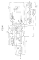
- the frame format conversion apparatus comprises a scanning format conversion circuit 100, a scanning line conversion circuit 200, a horizontal pixel conversion circuit 300 and a format control circuit 400.
- the scanning format conversion circuit 100 is adapted to convert a scanning format of an input video signal Vi into a progressive scanning type under control of the format control circuit 400 if it is of an interlaced scanning type and output the video signal of the converted scanning format to the scanning line conversion circuit 200.
- the scanning line conversion circuit 200 is adapted to convert the number of vertical scanning lines of the video signal from the scanning format conversion circuit 100 into that of a display format of a monitor under the control of the format control circuit 400.
- the scanning line conversion circuit 200 includes a 3:4 line converter 210 for converting the number of the vertical scanning lines of the video signal from the scanning format conversion circuit 100 into 1050 under the control of the format control circuit 400 if it is 787.5, a 4:3 line converter 220 for converting the number of the vertical scanning lines of the video signal from the scanning format conversion circuit 100 into 787.5 under the control of the format control circuit 400 if it is 1050, a 2:1 line converter 230 for converting the number of the vertical scanning lines of the video signal from the scanning format conversion circuit 100 into 525 under the control of the format control circuit 400 if it is 1050, and a 3:2 line converter 240 for converting the number of the vertical scanning lines of the video signal from the scanning format conversion circuit 100 into 525 under the control of the format control circuit 400 if it is 1050
- the horizontal pixel conversion circuit 300 is adapted to convert the number of horizontal pixels of an output video signal from the scanning line conversion circuit 200 into that of the display format of the monitor under the control of the format control circuit 400.
- the horizontal pixel conversion circuit 300 includes a 3:4 pixel converter 310 for converting the number of horizontal pixels of an output video signal from the 3:4 line converter 210 in the scanning line conversion circuit 200 at a ratio of 3:4 under the control of the format control circuit 400, a 4:3 pixel converter 320 for converting the number of horizontal pixels of an output video signal from the 4:3 line converter 220 in the scanning line conversion circuit 200 at a ratio of 4:3 under the control of the format control circuit 400, a 2:1 pixel converter 330 for converting the number of horizontal pixels of an output video signal from the 2:1 line converter 230 in the scanning line conversion circuit 200 at a ratio of 2:1 under the control of the format control circuit 400, and a 3:2 pixel converter 340 for converting the number of horizontal pixels of an output video signal from the 3:2 line
- the format control circuit 400 is adapted to control the scanning format conversion circuit 100, the 3:4 line converter 210, the 4:3 line converter 220, the 2:1 line converter 230 and the 3:2 line converter 240 in the scanning line conversion circuit 200, and the 3:4 pixel converter 310, the 4:3 pixel converter 320, the 2:1 pixel converter 330 and the 3:2 pixel converter 340 in the horizontal pixel conversion circuit 300 to convert a frame format of the input video signal Vi into the display format of the monitor.
- the format control circuit 400 controls automatically the conversion of the frame format of the input video signal Vi in response to a control signal designating the frame format of the input video signal Vi, transmitted from a broadcasting station, and the display format of the monitor. Alternatively, the frame format conversion may directly be controlled by the user as occasion demands.
- the scanning format conversion circuit 100, the 3:4 line converter 210, the 4:3 line converter 220, the 2:1 line converter 230 and the 3:2 line converter 240 in the scanning line conversion circuit 200, and the 3:4 pixel converter 310, the 4:3 pixel converter 320, the 2:1 pixel converter 330 and the 3:2 pixel converter 340 in the horizontal pixel conversion circuit 300 are selectively enabled by the format control circuit 400 on the basis of the frame format of the input video signal Vi and the display format of the monitor. Then, the enabled devices are operated to convert the frame format of the input video signal Vi into the display format of the monitor and output the video signal of the converted frame format to the monitor.
- the 3:4 line converter 210 and the 3:4 pixel converter 310 are enabled by the format control circuit 400 to convert the number of the vertical scanning lines and the number of the horizontal pixels of the input video signal Vi into those of the display format of the monitor and output the video signal of the converted frame format to the monitor.
- the 4:3 line converter 220 and the 4:3 pixel converter 320 are enabled by the format control circuit 400 to convert the number of the vertical scanning lines and the number of the horizontal pixels of the input video signal Vi into those of the display format of the monitor and output the video signal of the converted frame format to the monitor.
- the 2:1 line converter 230 and the 2:1 pixel converter 330 are enabled by the format control circuit 400 to convert the number of the vertical scanning lines and the number of the horizontal pixels of the input video signal Vi into those of the display format of the monitor and output the video signal of the converted frame format to the monitor.
- the 3:2 line converter 240 and the 3:2 pixel converter 340 are enabled by the format control circuit 400 to convert the number of the vertical scanning lines and the number of the horizontal pixels of the input video signal Vi into those of the display format of the monitor and output the video signal of the converted frame format to the monitor.
- the scanning format conversion circuit 100, the 4:3 line converter 220 and the 4:3 pixel converter 320 are enabled by the format control circuit 400 to convert the scanning format, the number of the vertical scanning lines and the number of the horizontal pixels of the input video signal Vi into those of the display format of the monitor and output the video signal of the converted frame format to the monitor.
- the scanning format conversion circuit 100, the 2:1 line converter 230 and the 2:1 pixel converter 330 are enabled by the format control circuit 400 to convert the scanning format, the number of the vertical scanning lines and the number of the horizontal pixels of the input video signal Vi into those of the display format of the monitor and output the video signal of the converted frame format to the monitor.
- the scanning format conversion circuit 100 includes a line average calculation circuit 101 for delaying the input video signal Vi and calculating an average of pixels in the same positions of upper and lower lines of the input video signal Vi, a first-in-first-out (FIFO) memory 102 for storing temporarily the delayed video signal from the line average calculation circuit 101, an FIFO memory 103 for storing temporarily the calculated average from the line average calculation circuit 101, and a multiplexer 104 for selecting alternately output signals from the FIFO memories 102 and 103.
- the scanning format conversion circuit 100 converts the interlaced scanning format into the progressive scanning format by interpolating the average of the pixels in the same positions of the upper and lower lines of the input video signal Vi into the input video signal Vi.
- the line average calculation circuit 101 includes a line memory 105 for storing and delaying the input video signal Vi in the unit of line and outputting the delayed video signal to the FIFO memory 102, an adder 106 for adding the delayed video signal from the line memory 105 to the input video signal Vi, and a divider 107 for dividing an output signal from the adder 106 by 2 and outputting the divided signal to the FIFO memory 103.
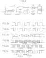
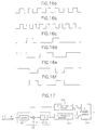
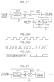
- Figs. 3A to 3F are waveform diagrams of the signals from the components in Fig. 2.
- the input video signal Vi as shown in Fig. 3C is stored and delayed in the unit of the line by the line memory 105 and then applied to the FIFO memory 102, a read operation of which is performed in response to an input line clock as shown in Fig. 3A, which controls input timing of the video signal.
- the delayed video signal from the line memory 105 is also applied to the adder 106, which also receives the input video signal Vi directly.
- the adder 106 adds the pixels in the same positions of the upper and lower lines of the input video signal Vi together by adding the delayed video signal from the line memory 105 to the input video signal Vi.
- the output signal from the adder 106 is divided by 2 by the divider 107 and then applied to the FIFO memory 103, a read operation of which is performed in response to an inverted one (Fig. 3B) of the input line clock as shown in Fig. 3A.
- the output signals from the FIFO memories 102 and 103 as shown in Figs. 3D and 3E are alternately selected by the multiplexer 104 and then outputted as shown in Fig. 3F.
- an odd line between adjacent even lines or an even line between adjacent odd lines is interpolated with an average of the adjacent lines. Namely, every input line is interpolated with the average of the upper and lower lines. In this manner, the scanning format of the input video signal is converted from the interlaced scanning type into the progressive scanning type.
- the scanning format conversion circuit 100 includes a line average calculation circuit 110, a frame average calculation circuit 120, a motion detection circuit 130 and an output signal selection circuit 140.
- the frame average calculation circuit 120 is adapted to calculate an average of pixels in the same positions of preceding and following frames of the input video signal Vi.
- the frame average calculation circuit 120 includes a field memory 121 for storing the input video signal Vi in the unit of field, a field memory 122 for storing an output signal from the field memory 121 in the unit of the field, an adder 123 for adding an output signal from the field memory 122 to the input video signal Vi, and a divider 124 for dividing an output signal from the adder 123 by 2.
- the line average calculation circuit 110 is adapted to calculate an average of pixels in the same positions of upper and lower lines of the input video signal Vi.
- the line average calculation circuit 110 includes a line memory 111 for storing and delaying the output signal from the field memory 121 in the frame average calculation circuit 120 in the unit of line, an adder 112 for adding an output signal from the line memory 111 to the output signal from the field memory 121, and a divider 113 for dividing an output signal from the adder 112 by 2.
- the motion detection circuit 130 is adapted to detect a motion of the input video signal Vi in response to output signals from the frame average calculation circuit 120 and the line average calculation circuit 110.
- the motion detection circuit 130 includes a subtracter 131 for calculating a difference between the output signal from the field memory 121 in the frame average calculation circuit 120 and the output signal from the line memory 111 in the line average calculation circuit 110, a subtracter 133 for calculating a difference between an output signal from the divider 124 in the frame average calculation circuit 120 and an output signal from the divider 113 in the line average calculation circuit 110, a comparator 132 for comparing an output signal from the subtracter 131 with a predetermined threshold value T1, a comparator 134 for comparing an output signal from the subtracter 133 with a predetermined threshold value T2, and an AND gate 135 for ANDing output signals from the comparators 132 and 134.
- the output signal selection circuit 140 is adapted to select one of the output signals from the frame average calculation circuit 120 and the line average calculation circuit 110 under control of the motion detection circuit 130 and output alternately the selected signal and the input video signal Vi.
- the output signal selection circuit 140 includes a multiplexer 141 for selecting one of the output signal from the divider 124 in the frame average calculation circuit 120 and the output signal from the divider 113 in the line average calculation circuit 110 under control of the AND gate 135 in the motion detection circuit 130, an FIFO memory 142 for storing temporarily an output signal from the multiplexer 141, an FIFO memory 143 for storing temporarily the output signal from the line memory 111 in the line average calculation circuit 110, and a multiplexer 144 for selecting one of output signals from the FIFO memories 142 and 143.
- Fig. 5 is a flowchart illustrating the operation of the scanning format conversion circuit 100 in Fig. 4 in accordance with the present invention.
- the input video signal Vi is sequentially stored in the unit of the field by the field memories 121 and 122 and then applied to the adder 123, which also receives the input video signal Vi directly.
- the adder 123 adds the output signal from the field memory 122 to the input video signal Vi.
- the divider 124 obtains the average (
- the output signal from the field memory 121 is also applied to the line average calculation circuit 110.
- the output signal from the field memory 121 is stored in the unit of the line by the line memory 111 and then applied to the adder 112, which also receives the output signal from the field memory 121 directly.
- the adder 112 adds the output signal from the line memory 111 to the output signal from the field memory 121.
- the divider 113 obtains the average (
- the subtracter 133 calculates the difference X2 between the average (
- X2
- the subtracter 131 calculates the difference X1 between the output signal from the field memory 121 in the frame average calculation circuit 120 and the output signal from the line memory 111 in the line average calculation circuit 110, namely, the difference between the pixels in the same positions of the adjacent upper and lower lines of the input video signal Vi.
- X1
- the calculated differences X1 and X2 from the subtracters 131 and 133 are compared with the predetermined threshold values T1 and T2 by the comparators 132 and 134, respectively. Then, the compared results from the comparators 132 and 134 are applied to the AND gate 135. That is, it is discriminated at the step 160 whether the difference X1 from the subtracter 131 is smaller than the predetermined threshold value T1. It is also discriminated at the step 160 whether the difference X2 from the subtracter 133 is smaller than the predetermined threshold value T2.
- the present video portion is determined as the still one.
- the present video portion is interpolated with the average (
- the present video portion is determined as the motion one. As a result, the present video portion is interpolated with the average (
- the multiplexer 141 is operated in response to the output signal from the AND gate 135 in the motion detection circuit 130 to select one of the output signal from the divider 124 or the average (
- the output signal from the multiplexer 141 is temporarily stored in the FIFO memory 142 and the output signal from the line memory 111 is temporarily stored in the FIFO memory 143.
- the multiplexer 144 selects alternately the output signals from the FIFO memories 142 and 143. In this manner, the scanning format of the input video signal is converted from the interlaced scanning type into the progressive scanning type.
- the 3:4 line converter 210 includes a filtering circuit 211, a signal output circuit 212 and an output controller 213.
- the filtering circuit 211 is adapted to delay and filter the video signal from the scanning format conversion circuit 100.
- the filtering circuit 211 includes a line memory 2111 for storing and delaying the video signal from the scanning format conversion circuit 100 in the unit of line and outputting the delayed video signal to the signal output circuit 212, an adder 2112 for adding an output signal from the line memory 2111 to the video signal from the scanning format conversion circuit 100, and a divider 2113 for dividing an output signal from the adder 2112 by 2 to obtain an average of pixels in the same positions of adjacent lines of the video signal from the scanning format conversion circuit 100 and outputting the divided signal to the signal output circuit 212.
- the signal output circuit 212 is adapted to select one of a plurality of output signals from the filtering circuit 211 and output the selected signal to the 3:4 pixel converter 310.
- the signal output circuit 212 includes an FIFO memory 2121 for storing temporarily the output signal from the line memory 2111 in the filtering circuit 211, an FIFO memory 2122 for storing temporarily an output signal from the divider 2113 in the filtering circuit 211, and a multiplexer 2123 for selecting one of output signals from the FIFO memories 2121 and 2122.
- the output controller 213 is adapted to control the signal output circuit 212 in response to input/output line clocks for controlling input/output timing of the video signal.
- the output controller 213 includes a line counter 2131 for counting the output line clock in the unit of 2 bits, a line counter 2132 for counting the input line clock in the unit of the 2 bits, an OR gate 2133 for ORing two output bits from the line counter 2131 and outputting the ORed signal to the FIFO memory 2122 and the multiplexer 2123 in the signal output circuit 212, a NOR gate 2134 for NORing two output bits from the line counter 2132 and outputting the NORed signal to the FIFO memory 2121 in the signal output circuit 212, and a NOT gate 2135 for inverting an output signal from the OR gate 2133 and outputting the inverted signal to the FIFO memory 2121 in the signal output circuit 212.
- Figs. 7A to 7E are waveform diagrams of the signals from the components in Fig. 6.
- the video signal from the scanning format conversion circuit 100 is stored and delayed in the unit of the line by the line memory 2111 and then applied to the adder 2112, which also receives the video signal from the scanning format conversion circuit 100 directly.
- the adder 2112 adds the output signal from the line memory 2111 to the video signal from the scanning format conversion circuit 100.
- the divider 2113 obtains the average of the pixels in the same positions of the adjacent lines of the video signal from the scanning format conversion circuit 100 by dividing the output signal from the adder 2112 by 2.
- the output signals from the line memory 2111 and the divider 2113 are temporarily stored in the FIFO memories 2121 and 2122 in the signal output circuit 212, respectively.
- the output line clock as shown in Fig. 7A is counted in the unit of the 2 bits by the line counter 2131.
- the two output bits from the line counter 2131 are ORed by the OR gate 2133, which thus outputs the ORed signal as shown in Fig. 7E.
- a read operation of the FIFO memory 2122 in the signal output circuit 212 and the operation of the multiplexer 2123 therein are controlled.
- the output signal from the OR gate 2133 is inverted as shown in Fig. 7D by the NOT gate 2135 and then applied to the FIFO memory 2121 in the signal output circuit 212 for the control of a read operation thereof.
- the input line clock as shown in Fig. 7B is counted in the unit of the 2 bits by the line counter 2132.
- the two output bits from the line counter 2132 are NORed by the NOR gate 2134, which thus outputs the NORed signal as shown in Fig. 7C to the FIFO memory 2121 in the signal output circuit 212 for the control of a write operation thereof.
- the output signals from the NOR gate 2134, the NOT gate 2135 and the OR gate 2133 as shown in Figs. 7C, 7D and 7E are adapted to control the FIFO memories 2121 and 2122 and the multiplexer 2123, thereby causing the number of the vertical scanning lines to be converted from 787.5 into 1050. Namely, only a first one of successive three lines of the video signal from the line memory 2111 is written into the FIFO memory 2121 in response to the output signal from the NOT gate as shown in Fig. 7C.
- the first line stored in the FIFO memory 2121 and the pixel average stored in the FIFO memory 2122 are alternately read according to the output timing based on the output signals from the NOT gate 2135 and the OR gate 2133 as shown in Figs. 7D and 7E.
- the signal which is outputted from the multiplexer 2123 in response to the output signal from the OR gate 2133 as shown in Fig. 7E consists of four lines, the first line from the FIFO memory 2121 and successive three lines of the pixel average from the FIFO memory 2122. Therefore, the number of the vertical scanning lines is converted from 787.5 into 1050.
- sequentially outputted from the multiplexer 2123 are the first input line, the average of the pixels in the same positions of the first and second input lines, the average of the pixels in the same positions of the second and third input lines, and the average of the pixels in the same positions of the third and fourth input lines.
- the 3:4 pixel converter 310 includes a filtering circuit 311 for delaying and filtering the video signal from the 3:4 line converter 210, a 1:3 demultiplexer 312 for 1:3-demultiplexing the filtered video signal from the filtering circuit 311, and a 4:1 multiplexer 313 for 4:1-multiplexing the delayed video signal from the filtering circuit 311 and output signals from the 1:3 demultiplexer 312.
- the filtering circuit 311 includes a latch 3111 for storing and delaying the video signal from the 3:4 line converter 210 in the unit of pixel and outputting the delayed video signal to the 4:1 multiplexer 313, an adder 3112 for adding an output signal from the latch 3111 to the video signal from the 3:4 line converter 210, and a divider 3113 for dividing an output signal from the adder 3112 by 2 to obtain an average of adjacent pixels of the video signal from the 3:4 line converter 210 and outputting the divided signal to the 1:3 demultiplexer 312.
- the video signal from the 3:4 line converter 210 is stored and delayed in the unit of the pixel by the latch 3111 and then applied to the adder 3112, which also receives the video signal from the 3:4 line converter 210 directly.
- the adder 3112 adds the output signal from the latch 3111 to the video signal from the 3:4 line converter 210.
- the divider 3113 obtains the average of the adjacent pixels, or left and right pixels, of the video signal from the 3:4 line converter 210 by dividing the output signal from the adder 3112 by 2.
- the pixel average from the divider 3113 is 1:3-demultiplexed by the 1:3 demultiplexer 312 and then applied to the 4:1 multiplexer 313, which also receives the output signal from the latch 3111.
- the 4:1 multiplexer 313 selects alternately the output signal from the latch 3111 and the three output signals from the 1:3 demultiplexer 312. As a result, the number of pixels per line is converted at the ratio of 3:4.
- sequentially outputted from the 4:1 multiplexer 313 are the first input pixel, the average of the first and second input pixels, the average of the second and third input pixels, and the average of the third and fourth input pixels.
- the 3:4 line converter 210 includes a coefficient generation circuit 216, a filtering circuit 214 and a signal output circuit 215.
- the coefficient generation circuit 216 is adapted to generate two filtering coefficients K1 and K2 in response to an input line clock for controlling input timing of the video signal and a synchronous signal.
- the coefficient generation circuit 216 includes a line counter 2161 for counting the input line clock in the unit of 2 bits in response to the synchronous signals a multiplexer 2162 for selecting one of three input coefficients A1, B1 and C1 in response to two output bits S1 and S2 from the line counter 2161 and outputting the selected input coefficient as the filtering coefficient K1 to the filtering circuit 214, and a multiplexer 2163 for selecting one of three input coefficients D1, E1 and F1 in response to the two output bits S1 and S2 from the line counter 2161 and outputting the selected input coefficient as the filtering coefficient K2 to the filtering circuit 214.
- the filtering circuit 214 is adapted to filter the video signal from the scanning format conversion circuit 100 using a weighted average in consideration of a relative position of an output line with respect to an input line in response to the filtering coefficients K1 and K2 from the coefficient generation circuit 216.
- the filtering circuit 214 includes a line memory 2141 for storing and delaying the video signal from the scanning format conversion circuit 100 in the unit of line, a multiplier 2142 for multiplying an output signal from the line memory 2141 by the filtering coefficient K1 from the multiplexer 2162 in the coefficient generation circuit 216, a multiplier 2144 for multiplying the video signal from the scanning format conversion circuit 100 by the filtering coefficient K2 from the multiplexer 2163 in the coefficient generation circuit 216, and an adder 2143 for adding output signals from the multipliers 2142 and 2144 and outputting the added signal to the signal output circuit 215.
- a line memory 2141 for storing and delaying the video signal from the scanning format conversion circuit 100 in the unit of line
- a multiplier 2142 for multiplying an output signal from the line memory 2141 by the filtering coefficient K1 from the multiplexer 2162 in the coefficient generation circuit 216
- a multiplier 2144 for multiplying the video signal from the scanning format conversion circuit 100 by the filtering coefficient K2 from the multiplexer 2163 in
- the signal output circuit 215 is adapted to selectively output a plurality of output signals from the filtering circuit 214.
- the signal output circuit 215 includes an FIFO memory 2151 for storing temporarily the output signal from the line memory 2141 in the filtering circuit 214, an FIFO memory 2152 for storing temporarily an output signal from the adder 2143 in the filtering circuit 214, a multiplexer 2153 for selecting one of output signals from the FIFO memories 2151 and 2152, and an output controller 2154 for controlling the FIFO memories 2151 and 2152 and the multiplexer 2153 in response to the input line clock.
- the input line clock controlling the input timing of the video signal is counted in the unit of the 2 bits by the line counter 2161 in response to the synchronous signal.
- the two output bits S1 and S2 from the line counter 2161 are applied to the multiplexer 2162, thereby causing the multiplexer 2162 to select one of the input coefficients A1, B1 and C1 and output the selected coefficient as the filtering coefficient K1 to the multiplier 2142 in the filtering circuit 214.
- the two output bits S1 and S2 from the line counter 2161 are also applied to the multiplexer 2163, thereby causing the multiplexer 2163 to select one of the input coefficients D1, E1 and F1 and output the selected coefficient as the filtering coefficient K2 to the multiplier 2144 in the filtering circuit 214.
- the sum of the filtering coefficients K1 and K2 from the multiplexers 2162 and 2163 always becomes "1". Namely, at a period of three lines, the filtering coefficient K1 becomes sequentially 0.25, 0.5 and 0.75, while the filtering coefficient K2 becomes sequentially 0.75, 0.5 and 0.25, resulting in insertion of the first input line in the unit of the three lines.
- the line counter 2161 is reset, thereby allowing the multiplexers 2162 and 2163 to sequentially select the input coefficients A1, B1 and C1, and D1, E1 and F1 in the unit of the three lines.
- the video signal from the scanning format conversion circuit 100 is multiplied by the filtering coefficient K2 from the multiplexer 2163 by the multiplier 2144 and then applied to the adder 2143. Also, the video signal from the scanning format conversion circuit 100 is stored and delayed in the unit of the line by the line memory 2141, multiplied by the filtering coefficient K1 from the multiplexer 2162 by the multiplier 2142 and then applied to the adder 2143.
- the adder 2143 obtains the weighted average in consideration of the relative position of the output line with respect to the input line by adding the output signals from the multipliers 2142 and 2144. Then, in the signal output circuit 215, the output signal from the line memory 2141 is temporarily stored in the FIFO memory 2151 and the output signal from the adder 2143 is temporarily stored in the FIFO memory 2152 under the control of the output controller 2154.
- the multiplexer 2153 is operated under the control of the output controller 2154 to output sequentially the first input line from the FIFO memory 2151, the weighted average of the first and second input lines from the FIFO memory 2152, the weighted average of the second and third input lines from the FIFO memory 2152, and the weighted average of the third and first input lines from the FIFO memory 2152.
- the output controller 2154 includes a 2-bit counter 2155 for counting the input line clock in the unit of the 2 bits, and an OR gate 2156 for ORing two output bits from the 2-bit counter 2155.
- the input line clock is counted in the unit of the 2 bits by the 2-bit counter 2155.
- the two output bits from the 2-bit counter 2155 are ORed by the OR gate 2156 and then applied to the FIFO memories 2151 and 2152 and the multiplexer 2153 to control them.
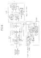
- the 3:4 line converter 210 includes a line memory 217, a weighted average calculation circuit 218, a line counter 219 and a signal output circuit 215'.
- the line memory 217 is adapted to store and delay the video signal from the scanning format conversion circuit 100 in the unit of line.
- the weighted average calculation circuit 218 is adapted to calculate a weighted average in consideration of a relative position of an output line with respect to an input line in response to the video signal from the scanning format conversion circuit 100 and an output signal from the line memory 217.
- the weighted average calculation circuit 218 includes a 4-divider 2181 for dividing the video signal from the scanning format conversion circuit 100 by 4, a 2-divider 2182 for dividing the video signal from the scanning format conversion circuit 100 by 2, an adder 2183 for adding output signals from the 4-divider 2181 and the 2-divider 2182, a multiplexer 2184 for selecting one of the output signals from the 4-divider 2181 and the 2-divider 2182 and an output signal from the adder 2183 under control of the line counter 219, a 4-divider 2185 for dividing the output signal from the line memory 217 by 4, a 2-divider 2186 for dividing the output signal from the line memory 217 by 2, an adder 2187 for adding output signals from the 4-divider 2185 and the 2-divider 2186, a multiplexer 2188 for selecting
- the line counter 219 is adapted to count an input line clock for controlling input timing of the video signal in the unit of 2 bits in response to a synchronous signal and control the multiplexers 2184 and 2188 in the weighted average calculation circuit 218 in accordance with the counted result.
- the line counter 219 is reset upon inputting three of the input line clocks.
- the signal output circuit 215' has the same construction and operation as those of the signal output circuit 215 in Fig. 9. Namely, the signal output circuit 215' is adapted to selectively output the output signal from the line memory 217 and an output signal from the weighted average calculation circuit 218.
- the signal output circuit 215' includes an FIFO memory 2151' for storing temporarily the output signal from the line memory 217, an FIFO memory 2152' for storing temporarily an output signal from the adder 2189 in the weighted average calculation circuit 218, a multiplexer 2153' for selecting one of output signals from the FIFO memories 2151' and 2152', and an output controller 2154' for controlling the FIFO memories 2151' and 2152' and the multiplexer 2153' in response to the input line clock.
- the output controller 2154' has the same construction and operation as those of the output controller 2154 in Fig. 10 and details thereof will thus be omitted.
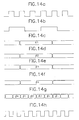
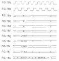
- Figs. 12A to 12F are waveform diagrams of the signals from the components in Fig. 11.
- the video signal from the scanning format conversion circuit 100 as shown in Fig. 12B is divided by 4 by the 4-divider 2181 and also divided by 2 by the 2-divider 2182.
- the output signals from the 4-divider 2181 and the 2-divider 2182 are added by the adder 2183 and then applied to the multiplexer 2184.
- the video signal from the scanning format conversion circuit 100 as shown in Fig. 12B is stored and delayed in the unit of the line by the line memory 217 and then applied to the weighted average calculation circuit 218. Then, in the weighted average calculation circuit 218, the output signal from the line memory 217 is divided by 4 by the 4-divider 2185 and also divided by 2 by the 2-divider 2186. The output signals from the 4-divider 2185 and the 2-divider 2186 are added by the adder 2187 and then applied to the multiplexer 2188.
- the multiplexers 2184 and 2188 sequentially select the output signals from the 4-divider 2181 and the adder 2187, the output signals from the 2-divider 2182 and the 2-divider 2186 and the output signals from the adder 2183 and the 4-divider 2185 to the adder 2189 as shown in Figs. 12F and 12E.
- the output signal from the 4-divider 2181 is the same as the result obtained by multiplying the video signal from the scanning format conversion circuit 100 by a filtering coefficient of 0.25.
- the output signal from the 2-divider 2182 is the same as the result obtained by multiplying the video signal from the scanning format conversion circuit 100 by a filtering coefficient of 0.5.
- the output signal from the adder 2183 is the same as the result obtained by multiplying the video signal from the scanning format conversion circuit 100 by a filtering coefficient of 0.75.
- the output signal from the 4-divider 2185 is the same as the result obtained by multiplying the next line of the video signal from the line memory 217 by the filtering coefficient of 0.25.
- the output signal from the 2-divider 2186 is the same as the result obtained by multiplying the next line of the video signal from the line memory 217 by the filtering coefficient of 0.5.
- the output signal from the adder 2187 is the same as the result obtained by multiplying the next line of the video signal from the line memory 217 by the filtering coefficient of 0.75.
- the weighted average in consideration of the relative position of the output line with respect to the input line is obtained in such a manner that the signals making the sum of the filtering coefficients "1" are selected by the multiplexers 2184 and 2188 and then added by the adder 2189 under the control of the line counter 219.
- the input line clock as shown in Fig. 12A is counted in the unit of the 2 bits by the line counter 219 in response to the synchronous signal.
- the two output bits from the line counter 219 as shown in Figs. 12C and 12D are applied to the multiplexers 2184 and 2188 in the weighted average calculation circuit 218, thereby causing the multiplexers 2184 and 2188 to select the output signals from the 4-dividers 2181 and 2185, the 2-dividers 2182 and 2186 and the adders 2183 and 2187 in the weighted average calculation circuit 218 to make the sum of the filtering coefficients "1".
- the multiplexer 2184 selects alternately the output signals from the 4-divider 2181, the 2-divider 2182 and the adder 2183 at a period of three lines and the multiplexer 2188 selects alternately the output signals from the 4-divider 2185, the 2-divider 2186 and the adder 2187 at the period of the three lines.
- the multiplexer 2153' is operated under the control of the output controller 2154' to output sequentially the first input line from the FIFO memory 2151', the weighted average of the first and second input lines from the FIFO memory 2152', the weighted average of the second and third input lines from the FIFO memory 2152', and the weighted average of the third and first input lines from the FIFO memory 2152'.
- the 3:4 pixel converter 310 includes a coefficient generation circuit 316, a filtering circuit 314 and a signal output circuit 315.
- the coefficient generation circuit 316 is adapted to generate two filtering coefficients K3 and K4 in response to an input sample clock for controlling input timing of the video signal and a synchronous signal.
- the coefficient generation circuit 316 includes a 2-bit counter 3161 for counting the input sample clock in the unit of 2 bits in response to the synchronous signal, a multiplexer 3162 for selecting one of three input coefficients A2, B2 and C2 in response to two output bits S3 and S4 from the 2-bit counter 3161 and outputting the selected input coefficient as the filtering coefficient K3 to the filtering circuit 314, and a multiplexer 3163 for selecting one of three input coefficients D2, E2 and F2 in response to the two output bits S3 and S4 from the 2-bit counter 3161 and outputting the selected input coefficient as the filtering coefficient K4 to the filtering circuit 314.
- the filtering circuit 314 is adapted to filter the video signal from the 3:4 line converter 210 using a weighted average in consideration of a relative position of an output pixel with respect to an input pixel in response to the filtering coefficients K3 and K4 from the coefficient generation circuit 316.
- the filtering circuit 314 includes a latch 3141 for storing and delaying the video signal from the 3:4 line converter 210 in the unit of pixel, a multiplier 3142 for multiplying an output signal from the latch 3141 by the filtering coefficient K3 from the multiplexer 3162 in the coefficient generation circuit 316, a multiplier 3144 for multiplying the video signal from the 3:4 line converter 210 by the filtering coefficient K4 from the multiplexer 3163 in the coefficient generation circuit 316, and an adder 3143 for adding output signals from the multipliers 3142 and 3144 and outputting the added signal to the signal output circuit 315.
- the signal output circuit 315 is adapted to select one of a plurality of output signals from the filtering circuit 314.
- the signal output circuit 315 includes a latch 3151 for storing temporarily and delaying the output signal from the latch 3141 in the filtering circuit 314, a 1:3 demultiplexer 3152 for 1:3-demultiplexing an output signal from the adder 3143 in the filtering circuit 314, a latch 3153 for storing temporarily and delaying an output signal from the latch 3151, a latch 3154 for storing temporarily and delaying a first output signal from the 1:3 demultiplexer 3152, a latch 3155 for storing temporarily and delaying a second output signal from the 1:3 demultiplexer 3152, a latch 3156 for storing temporarily and delaying an output signal from the latch 3154, and a 4:1 multiplexer 3157 for selectively outputting output signals from the latches 3153, 3155 and 3156 and a third output signal from the 1:3 demultiplexer 3152.
- Figs. 14A to 14H are waveform diagrams of the signals from the components in Fig. 13.
- the input sample clock as shown in Fig. 14A, controlling the input timing of the video signal is counted in the unit of the 2 bits by the 2-bit counter 3161 in response to the synchronous signal.
- the two output bits S3 and S4 from the 2-bit counter 3161 are applied to the multiplexer 3162, thereby causing the multiplexer 3162 to select one of the input coefficients A2, B2 and C2 and output the selected coefficient as the filtering coefficient K3 to the multiplier 3142 in the filtering circuit 314.
- the two output bits S3 and S4 from the 2-bit counter 3161 are also applied to the multiplexer 3163, thereby causing the multiplexer 3163 to select one of the input coefficients D2, E2 and F2 and output the selected coefficient as the filtering coefficient K4 to the multiplier 3144 in the filtering circuit 314.
- the sum of the filtering coefficients K3 and K4 from the multiplexers 3162 and 3163 always becomes "1". Namely, at a period of three pixels, the filtering coefficient K3 becomes sequentially 0.25, 0.5 and 0.75, while the filtering coefficient K4 becomes sequentially 0.75, 0.5 and 0.25, resulting in insertion of the first input pixel in the unit of the three pixels.
- the 2-bit counter 3161 is reset, thereby allowing the multiplexers 3162 and 3163 to sequentially select the input coefficients A2, B2 and C2, and D2, E2 and F2 in the unit of the three pixels.
- the video signal from the 3:4 line converter 210 is multiplied by the filtering coefficient K4 from the multiplexer 3163 by the multiplier 3144 and then applied to the adder 3143. Also, the video signal from the 3:4 line converter 210 is stored and delayed in the unit of the pixel by the latch 3141, multiplied by the filtering coefficient K3 from the multiplexer 3162 by the multiplier 3142 and then applied to the adder 3143.
- the adder 3143 obtains the weighted average in consideration of the relative position of the output pixel with respect to the input pixel by adding the output signals from the multipliers 3142 and 3144. Then, in the signal output circuit 315, the output signal from the adder 3143 is 1:3-demultiplexed by the 1:3 demultiplexer 3152. Then, the third one of the three output signals from the 1:3 demultiplexer 3152 as shown in Fig. 14F is directly applied to the 4:1 multiplexer 3157.
- the output signal from the latch 3141 in the filtering circuit 314 is temporarily stored in the latch 3151, temporarily stored in the latch 3153 and then applied to the 4:1 multiplexer 3157 in the form as shown in Fig. 14C.
- the second output signal from the 1:3 demultiplexer 3152 is temporarily stored in the latch 3155 and then applied to the 4:1 multiplexer 3157 in the form as shown in Fig. 14D.
- the first output signal from the 1:3 demultiplexer 3152 is temporarily stored in the latch 3154, temporarily stored in the latch 3156 and then applied to the 4:1 multiplexer 3157 in the form as shown in Fig. 14E.
- the 4:1 multiplexer 3157 outputs sequentially the weighted average of the third and first input pixels from the 1:3 demultiplexer 3152 as shown in Fig. 14F, the first input pixel from the latch 3153 as shown in Fig. 14C, the weighted average of the first and second input pixels from the latch 3155 as shown in Fig. 14D and the weighted average of the second and third input pixels from the latch 3156 as shown in Fig. 14E.
- the 4:3 line converter 220 includes a filtering circuit 221, a signal output circuit 222 and an output controller 223.
- the filtering circuit 221 is adapted to delay and filter the video signal from the scanning format conversion circuit 100.
- the filtering circuit 221 includes a line memory 2211 for storing and delaying the video signal from the scanning format conversion circuit 100 in the unit of line and outputting the delayed video signal to the signal output circuit 222, an adder 2212 for adding an output signal from the line memory 2211 to the video signal from the scanning format conversion circuit 100, and a divider 2213 for dividing an output signal from the adder 2212 by 2 to obtain an average of pixels in the same positions of adjacent lines of the video signal from the scanning format conversion circuit 100 and outputting the divided signal to the signal output circuit 222.
- the signal output circuit 222 is adapted to selectively output a plurality of output signals from the filtering circuit 221.
- the signal output circuit 222 includes an FIFO memory 2221 for storing temporarily the output signal from the line memory 2211 in the filtering circuit 221, an FIFO memory 2222 for storing temporarily an output signal from the divider 2213 in the filtering circuit 221, and a multiplexer 2223 for outputting selectively output signals from the FIFO memories 2221 and 2222.
- the output controller 223 is adapted to control the signal output circuit 222 in response to input/output line clocks for controlling input/output timing of the video signal.
- the output controller 223 includes a line counter 2231 for counting the input line clock in the unit of 2 bits, a line counter 2232 for counting the output line clock in the unit of the 2 bits, a NOT gate 2233 for inverting a first output bit S5 from the line counter 2231, a NOR gate 2235 for NORing an output signal from the NOT gate 2233 and a second output bit S6 from the line counter 2231 and outputting the NORed signal to the FIFO memory 2222 in the signal output circuit 222 for the control of a write operation thereof, a latch 2238 for storing temporarily the second output bit S6 from the line counter 2231 for the control of a write operation of the FIFO memory 2221 in the signal output circuit 222, a NOT gate 2234 for inverting a first output bit S7 from the line counter 2232, an OR gate 2236 for OR
- Figs. 16A to 16F are waveform diagrams of the signals from the components in Fig. 15.
- the video signal from the scanning format conversion circuit 100 is stored and delayed in the unit of the line by the line memory 2211 and then applied to the adder 2212, which also receives the video signal from the scanning format conversion circuit 100 directly.
- the adder 2212 adds the output signal from the line memory 2211 to the video signal from the scanning format conversion circuit 100.
- the divider 2213 obtains the average of the pixels in the same positions of the adjacent lines of the video signal from the scanning format conversion circuit 100 by dividing the output signal from the adder 2212 by 2.
- the output signals from the line memory 2211 and the divider 2213 are temporarily stored in the FIFO memories 2221 and 2222 in the signal output circuit 222, respectively.
- the input line clock as shown in Fig. 16B is counted in the unit of the 2 bits by the line counter 2231.
- the first output bit S5 from the line counter 2231 is inverted by the NOT gate 2233 and then NORed by the NOR gate 2235 together with the second output bit S6 from the line counter 2231.
- the resultant signal from the NOR gate 2235 as shown in Fig. 16C is applied to the FIFO memory 2222 in the signal output circuit 222 for the control of the write operation thereof.
- the second output bit S6 from the line counter 2231 is temporarily stored in the latch 2238 and then applied to the FIFO memory 2221 in the signal output circuit 222 in the form as shown in Fig. 16D for the control of the write operation thereof.
- the output line clock as shown in Fig. 16A is counted in the unit of the 2 bits by the line counter 2232.
- the first output bit S7 from the line counter 2232 is inverted by the NOT gate 2234 and then ORed by the OR gate 2236 together with the second output bit S8 from the line counter 2232.
- the resultant signal from the OR gate 2236 as shown in Fig. 16E is applied to the FIFO memory 2221 in the signal output circuit 222 for the control of the read operation thereof.
- the output signal from the OR gate 2236 is inverted by the NOT gate 2237 and then applied to the FIFO memory 2222 in the signal output circuit 222 in the form as shown in Fig. 16F for the control of the read operation thereof.
- the output signal from the NOT gate 2237 as shown in Fig. 16F is also applied to the multiplexer 2223 in the signal output circuit 222 to control it.
- the output signals from the OR gate 2236 and the NOT gate 2237 as shown in Figs. 16E and 16F are adapted to control the reading operations of the FIFO memories 2221 and 2222 and the output of the multiplexer 2223.
- the first line and the average of the pixels in the same positions of the second and third lines are repeatedly outputted from the multiplexer 2223.
- sequentially outputted from the multiplexer 2223 are the first input line, the average of the pixels in the same positions of the second and third input lines, and the fourth input line. Therefore, the number of the vertical scanning lines is converted from 1050 into 787.5.
- the 4:3 pixel converter 320 includes a filtering circuit 321, 1:4 demultiplexers 322 and 323 and a 3:1 multiplexer 324.
- the filtering circuit 321 is adapted to delay and filter the video signal from the 4:3 line converter 220.
- the filtering circuit 321 includes a latch 3211 for storing and delaying the video signal from the 4:3 line converter 220 in the unit of pixel and outputting the delayed video signal to the 1:4 demultiplexer 322, an adder 3212 for adding an output signal from the latch 3211 to the video signal from the 4:3 line converter 220, and a divider 3213 for dividing an output signal from the adder 3212 by 2 to obtain an average of adjacent pixels of the video signal from the 4:3 line converter 220 and outputting the divided signal to the 1:4 demultiplexer 323.
- the 1:4 demultiplexer 322 is adapted to 1:4-demultiplex the delayed video signal from the latch 3211 in the filtering circuit 321.
- the 1:4 demultiplexer 323 is adapted to 1:4-demultiplex the filtered video signal from the divider 3213 in the filtering circuit 321.
- the 3:1 multiplexer 324 is adapted to 3:1-multiplex output signals from the 1:4 demultiplexers 322 and 323.
- Figs. 18A to 18K are waveform diagrams of the signals from the components in Fig. 17.
- the video signal from the 4:3 line converter 220 is stored and delayed in the unit of the pixel by the latch 3211 and then applied to the adder 3212, which also receives the video signal from the 4:3 line converter 220 directly.
- the adder 3212 adds the output signal from the latch 3211 to the video signal from the 4:3 line converter 220.
- the divider 3213 obtains the average of the adjacent pixels of the video signal from the 4:3 line converter 220 by dividing the output signal from the adder 3212 by 2.
- the output signal from the latch 3211 is also applied to the 1:4 demultiplexer 322.
- the 1:4 demultiplexer 322 outputs signals as shown in Figs. 18C-18F and the 1:4 demultiplexer 323 outputs signals as shown in Figs. 18G-18J.
- the 3:1 multiplexer 324 outputs selectively a part of the output signals from the 1:4 demultiplexers 322 and 323 in response to the output sample clock as shown in Fig. 18B. Namely, sequentially outputted from the 3:1 multiplexer 324 are the first input pixel, the average of the second and third input pixels, and the fourth input pixel, as shown in Fig. 18K.
- the 4:3 line converter 220 includes a coefficient generation circuit 226, a filtering circuit 224 and a signal output circuit 225.
- the coefficient generation circuit 226 is adapted to generate two filtering coefficients K5 and K6 in response to an input line clock for controlling input timing of the video signal and a synchronous signal.
- the coefficient generation circuit 226 includes a line counter 2261 for counting the input line clock in the unit of 2 bits in response to the synchronous signal, a multiplexer 2262 for selecting one of four input coefficients A3, B3, C3 and D3 in response to two output bits S9 and S10 from the line counter 2261 and outputting the selected input coefficient as the filtering coefficient K5 to the filtering circuit 224, and a multiplexer 2263 for selecting one of four input coefficients E3, F3, G3 and H3 in response to the two output bits S9 and S10 from the line counter 2261 and outputting the selected input coefficient as the filtering coefficient K6 to the filtering circuit 224.
- the filtering circuit 224 is adapted to filter the video signal from the scanning format conversion circuit 100 using a weighted average in consideration of a relative position of an output line with respect to an input line in response to the filtering coefficients K5 and K6 from the coefficient generation circuit 226.
- the filtering circuit 224 includes a line memory 2241 for storing and delaying the video signal from the scanning format conversion circuit 100 in the unit of line, a multiplier 2242 for multiplying an output signal from the line memory 2241 by the filtering coefficient K5 from the multiplexer 2262 in the coefficient generation circuit 226, a multiplier 2244 for multiplying the video signal from the scanning format conversion circuit 100 by the filtering coefficient K6 from the multiplexer 2263 in the coefficient generation circuit 226, and an adder 2243 for adding output signals from the multipliers 2242 and 2244 and outputting the added signal to the signal output circuit 225.
- the signal output circuit 225 is adapted to selectively output an output signal from the filtering circuit 224.
- the signal output circuit 225 includes an FIFO memory 2251 for storing temporarily an output signal from the adder 2243 in the filtering circuit 224, and an output controller 2252 for controlling a write operation of the FIFO memory 2251 in response to the input line clock.
- the input line clock controlling the input timing of the video signal is counted in the unit of the 2 bits by the line counter 2261 in response to the synchronous signal.
- the two output bits S9 and S10 from the line counter 2261 are applied to the multiplexer 2262, thereby causing the multiplexer 2262 to select one of the input coefficients A3, B3, C3 and D3 and output the selected coefficient as the filtering coefficient K5 to the multiplier 2242 in the filtering circuit 224.
- the two output bits S9 and S10 from the line counter 2261 are also applied to the multiplexer 2263, thereby causing the multiplexer 2263 to select one of the input coefficients E3, F3, G3 and H3 and output the selected coefficient as the filtering coefficient K6 to the multiplier 2244 in the filtering circuit 224.
- the sum of the filtering coefficients K5 and K6 from the multiplexers 2262 and 2263 always becomes "1". Namely, at a period of four lines, the filtering coefficient K5 becomes sequentially 1, 0.69, 0.31 and 0, while the filtering coefficient K6 becomes sequentially 0, 0.31, 0.69 and 1. For this reason, the fourth input line is removed in the unit of the four lines. Namely, the line corresponding to the filtering coefficients K5 and K6 of "1" is not needed. Therefore, the multiplexers 2262 and 2263 sequentially select the input coefficients A3, B3, C3 and D3, and E3, F3, G3 and H3 in the unit of the four lines.
- the video signal from the scanning format conversion circuit 100 is multiplied by the filtering coefficient K6 from the multiplexer 2263 by the multiplier 2244 and then applied to the adder 2243. Also, the video signal from the scanning format conversion circuit 100 is stored and delayed in the unit of the line by the line memory 2241, multiplied by the filtering coefficient K5 from the multiplexer 2262 by the multiplier 2242 and then applied to the adder 2243.
- the adder 2243 obtains the weighted average in consideration of the relative position of the output line with respect to the input line by adding the output signals from the multipliers 2242 and 2244. Then, in the signal output circuit 225, the output signal from the adder 2243 is temporarily stored in the FIFO memory 2251 and then applied to the 4:3 pixel converter 320 under the control of the output controller 2252.
- the output controller 2252 includes a 2-bit counter 2253 for counting the input line clock in the unit of the 2 bits, a NOT gate 2254 for inverting a first output bit S11 from the 2-bit counter 2253, a NOT gate 2255 for inverting a second output bit S12 from the 2-bit counter 2253, and an OR gate 2256 for ORing output signals from the NOT gates 2254 and 2255 and outputting the ORed signal to the FIFO memory 2251 for the control of the write operation thereof.
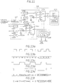
- Figs. 21A and 21B are waveform diagrams of the signals from the components in Fig. 20.
- the input line clock as shown in Fig. 21A is counted in the unit of the 2 bits by the 2-bit counter 2253.
- the two output bits S11 and S12 from the 2-bit counter 2253 are inverted by the NOT gates 2254 and 2255 and then ORed by the OR gate 2256.
- the output signal from the OR gate 2256 as shown in Fig. 21B is applied to the FIFO memory 2251 for the control of the write operation thereof.
- sequentially outputted from the FIFO memory 2251 are the first input line from the adder 2243, the weighted average of the first and second input lines from the adder 2243, and the weighted average of the second and third input lines from the adder 2243, while the fourth input line from the adder 2243 is removed.
- the 4:3 line converter 220 includes a line memory 227, a weighted average calculation circuit 228, a line counter 2296 and a signal output circuit 225'.
- the line memory 227 is adapted to store and delay the video signal from the scanning format conversion circuit 100 in the unit of line.
- the weighted average calculation circuit 228 is adapted to calculate a weighted average in consideration of a relative position of an output line with respect to an input line in response to the video signal from the scanning format conversion circuit 100 and an output signal from the line memory 227.
- the weighted average calculation circuit 228 includes a 16-divider 2281 for dividing the video signal from the scanning format conversion circuit 100 by 16, a 4-divider 2282 for dividing the video signal from the scanning format conversion circuit 100 by 4, a 2-divider 2283 for dividing the video signal from the scanning format conversion circuit 100 by 2, an adder 2284 for adding output signals from the 4-divider 2282 and the 2-divider 2283, an adder 2285 for adding an output signal from the 16-divider 2281 and the output signal from the 4-divider 2282, a subtracter 2286 for obtaining a difference between an output signal from the adder 2284 and the output signal from the 16-divider 2281, a multiplexer 2287 for selecting one of the video signal from the scanning format conversion circuit 100, output signals from the adder 2285 and the
- the line counter 2296 is adapted to count an input line clock controlling input timing of the video signal in the unit of 2 bits in response to a synchronous signal and control the multiplexers 2287 and 2294 in the weighted average calculation circuit 228 in accordance with the counted result.
- the signal output circuit 225' has the same construction and operation as those of the signal output circuit 225 in Fig. 19. Namely, the signal output circuit 225' is adapted to selectively output an output signal from the weighted average calculation circuit 228. To this end, the signal output circuit 225' includes an FIFO memory 2251' for storing temporarily an output signal from the adder 2295 in the weighted average calculation circuit 228, and an output controller 2252' for controlling a write operation of the FIFO memory 2251' in response to the input line clock. Also, the output controller 2252' has the same construction and operation as those of the output controller 2252 in Fig. 20 and details thereof will thus be omitted.
- Figs. 23A to 23F are waveform diagrams of the signals from the components in Fig. 22.
- the video signal from the scanning format conversion circuit 100 is stored and delayed in the unit of the line by the line memory 227 and then applied to the weighted average calculation circuit 228.
- the output signal from the line memory 227 as shown in Fig. 23B is divided by 16 by the 16-divider 2288, divided by 4 by the 4-divider 2289 and divided by 2 by the 2-divider 2290.
- the output signals from the 16-divider 2288 and the 4-divider 2289 are added by the adder 2292 and then applied to the multiplexer 2294.
- the output signals from the 4-divider 2289 and the 2-divider 2290 are added by the adder 2291 and then applied to the subtracter 2293, which also receives the output signal from the 16-divider 2288 directly.
- the subtracter 2293 obtains the difference between the output signal from the adder 2291 and the output signal from the 16-divider 2288 and outputs the obtained difference to the multiplexer 2294.
- the multiplexer 2294 inputs the output signal from the line memory 227, the output signals from the adder 2292 and the subtracter 2293 and the ground signal of "0".
- the output signal from the line memory 227 is the same as the result obtained by multiplying the output signal from the line memory 227 by a filtering coefficient of 1.
- the output signal from the subtracter 2293 is the same as the result obtained by multiplying the output signal from the line memory 227 by a filtering coefficient of 0.69.
- the output signal from the adder 2292 is the same as the result obtained by multiplying the output signal from the line memory 227 by a filtering coefficient of 0.31.
- the ground signal is the same as the result obtained by multiplying the output signal from the line memory 227 by a filtering coefficient of 0.
- the video signal from the scanning format conversion circuit 100 is applied to the weighted average calculation circuit 228.
- the video signal from the scanning format conversion circuit 100 is divided by 16 by the 16-divider 2281, divided by 4 by the 4-divider 2282 and divided by 2 by the 2-divider 2283.
- the output signals from the 16-divider 2281 and the 4-divider 2282 are added by the adder 2285 and then applied to the multiplexer 2287.
- the output signals from the 4-divider 2282 and the 2-divider 2283 are added by the adder 2284 and then applied to the subtracter 2286, which also receives the output signal from the 16-divider 2281 directly.
- the subtracter 2286 obtains the difference between the output signal from the adder 2284 and the output signal from the 16-divider 2281 and outputs the obtained difference to the multiplexer 2287.
- the multiplexer 2287 inputs the video signal from the scanning format conversion circuit 100, the output signals from the adder 2285 and the subtracter 2286 and the ground signal of "0".
- the video signal from the scanning format conversion circuit 100 is the same as the result obtained by multiplying the video signal from the scanning format conversion circuit 100 by the filtering coefficient of 1.
- the output signal from the subtracter 2286 is the same as the result obtained by multiplying the video signal from the scanning format conversion circuit 100 by the filtering coefficient of 0.69.
- the output signal from the adder 2285 is the same as the result obtained by multiplying the video signal from the scanning format conversion circuit 100 by the filtering coefficient of 0.31.
- the ground signal is the same as the result obtained by multiplying the video signal from the scanning format conversion circuit 100 by the filtering coefficient of 0.
- the multiplexers 2287 and 2294 sequentially select the ground signal and the output signal from the line memory 227, the output signals from the subtracter 2286 and the adder 2292, the output signals from the adder 2285 and the subtracter 2293, and the video signal from the scanning format conversion circuit 100 and the ground signal. Therefore, the weighted average in consideration of the relative position of the output line with respect to the input line is obtained in such a manner that the signals making the sum of the filtering coefficients "1" are selected by the multiplexers 2287 and 2294 and then added by the adder 2295 under the control of the line counter 2296.
- the input line clock as shown in Fig. 23A is counted in the unit of the 2 bits by the line counter 2296 in response to the synchronous signal.
- the two output bits from the line counter 2296 as shown in Figs. 23C and 23D are applied to the multiplexers 2287 and 2294 in the weighted average calculation circuit 228, thereby causing the multiplexers 2287 and 2294 to select the video signal from the scanning format conversion circuit 100, the output signal from the line memory 227, the ground signal and the output signals from the subtracters 2286 and 2293 and the adders 2285 and 2292 in the weighted average calculation circuit 228 to make the sum of the filtering coefficients "1".
- the multiplexer 2287 selects alternately the ground signal, the output signal from the subtracter 2286, the output signal from the adder 2285 and the video signal from the scanning format conversion circuit 100 at a period of four lines and the multiplexer 2294 selects alternately the output signal from the line memory 227, the output signal from the adder 2292, the output signal from the subtracter 2293 and the ground signal at the period of the four lines.
- the multiplexer 2294 outputs, as shown in Fig. 23E, a first one of successive four lines of the video signal, the resultant signal obtained by multiplying the second line by 0.69, the resultant signal obtained by multiplying the third line by 0.31 and the ground signal obtained by multiplying the fourth line by 0.
- the multiplexer 2287 outputs, as shown in Fig. 23F, the ground signal obtained by multiplying the second line by 0, the resultant signal obtained by multiplying the third line by 0.31, the resultant signal obtained by multiplying the fourth line by 0.69 and the first line.
- the output signals from the multiplexers 2294 and 2287 are added by the adder 2295 and then outputted through the FIFO memory 2251' in the signal output circuit 225'.
- sequentially outputted from the FIFO memory 2251' are the first input line, the weighted average of the pixels in the same positions of the first and second input lines, and the weighted average of the pixels in the same positions of the second and third input lines, while the fourth input line is not selected.
- the 4:3 pixel converter 320 includes a coefficient generation circuit 327, a filtering circuit 325 and a signal output circuit 326.
- the coefficient generation circuit 327 is adapted to generate two filtering coefficients K7 and K8 in response to an input sample clock for controlling input timing of the video signal and a synchronous signal.
- the coefficient generation circuit 327 includes a 2-bit counter 3271 for counting the input sample clock in the unit of 2 bits in response to the synchronous signal, a multiplexer 3272 for selecting one of four input coefficients A4, B4, C4 and D4 in response to two output bits S13 and S14 from the 2-bit counter 3271 and outputting the selected input coefficient as the filtering coefficient K7 to the filtering circuit 325, and a multiplexer 3273 for selecting one of four input coefficients E4, F4, G4 and H4 in response to the two output bits S13 and S14 from the 2-bit counter 3271 and outputting the selected input coefficient as the filtering coefficient K8 to the filtering circuit 325.
- the filtering circuit 325 is adapted to filter the video signal from the 4:3 line converter 220 using a weighted average in consideration of a relative position of an output pixel with respect to an input pixel in response to the filtering coefficients K7 and K8 from the coefficient generation circuit 327.
- the filtering circuit 325 includes a latch 3251 for storing and delaying the video signal from the 4:3 line converter 220 in the unit of pixel, a multiplier 3252 for multiplying an output signal from the latch 3251 by the filtering coefficient K7 from the multiplexer 3272 in the coefficient generation circuit 327, a multiplier 3254 for multiplying the video signal from the 4:3 line converter 220 by the filtering coefficient K8 from the multiplexer 3273 in the coefficient generation circuit 327, and an adder 3253 for adding output signals from the multipliers 3252 and 3254 and outputting the added signal to the signal output circuit 326.
- the signal output circuit 326 is adapted to selectively output an output signal from the filtering circuit 325 in response to the input sample clock and an output sample clock for controlling output timing of the video signal.
- the signal output circuit 326 includes a 1:4 demultiplexer 3261 for 1:4-demultiplexing an output signal from the adder 3253 in the filtering circuit 325, a 4:1 multiplexer 3262 for 4:1-multiplexing output signals from the 1:4 demultiplexer 3261, and an output controller 3263 for controlling the 1:4 demultiplexer 3261 and the 4:1 multiplexer 3262 in response to the input sample clock and the output sample clock.
- the output controller 3263 includes a 2-bit counter 3264 for counting the input sample clock in the unit of the 2 bits and providing two output bits S15 and S16 to control the 1:4 demultiplexer 3261 in accordance with the counted result, a 2-bit counter 3265 for counting the output sample clock in the unit of the 2 bits and providing two output bits S17 and S18 to control the 4:1 multiplexer 3262 in accordance with the counted result, a NOT gate 3266 for inverting the output bit S17 from the 2-bit counter 3265, and an AND gate 3267 for ANDing the output bit S18 from the 2-bit counter 3265 and an output signal from the NOT gate 3266 and outputting the ANDed signal to the 2-bit counter 3265 to control it.
- a 2-bit counter 3264 for counting the input sample clock in the unit of the 2 bits and providing two output bits S15 and S16 to control the 1:4 demultiplexer 3261 in accordance with the counted result
- a 2-bit counter 3265 for counting the output sample clock in the unit of the 2
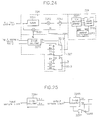
- Figs. 26A to 26H are waveform diagrams of the signals from the components in Fig. 24.
- the input sample clock as shown in Fig. 26A, controlling the input timing of the video signal is counted in the unit of the 2 bits by the 2-bit counter 3271 in response to the synchronous signal.
- the two output bits S13 and S14 from the 2-bit counter 3271 are applied to the multiplexer 3272, thereby causing the multiplexer 3272 to select one of the input coefficients A4, B4, C4 and D4 and output the selected coefficient as the filtering coefficient K7 to the multiplier 3252 in the filtering circuit 325.
- the two output bits S13 and S14 from the 2-bit counter 3271 are also applied to the multiplexer 3273, thereby causing the multiplexer 3273 to select one of the input coefficients E4, F4, G4 and H4 and output the selected coefficient as the filtering coefficient K8 to the multiplier 3254 in the filtering circuit 325.
- the sum of the filtering coefficients K7 and K8 from the multiplexers 3272 and 3273 always becomes "1". Namely, at a period of four pixels, the filtering coefficient K7 becomes sequentially 0, 0.31, 0.69 and 1, while the filtering coefficient K8 becomes sequentially 1, 0.69, 0.31 and 0. For this reason, the fourth input pixel is removed in the unit of the four pixels. To this end, upon the input of four of the input sample clocks, that is, before the input of the fifth pixel after the input of the four pixels, the 2-bit counter 3271 is reset, thereby allowing the multiplexers 3272 and 3273 to sequentially select the input coefficients A4, B4, C4 and D4, and E4, F4, G4 and H4 in the unit of the four pixels.
- the video signal from the 4:3 line converter 220 is multiplied by the filtering coefficient K8 from the multiplexer 3273 by the multiplier 3254 and then applied to the adder 3253. Also, the video signal from the 4:3 line converter 220 is stored and delayed in the unit of the pixel by the latch 3251, multiplied by the filtering coefficient K7 from the multiplexer 3272 by the multiplier 3252 and then applied to the adder 3253.
- the adder 3253 obtains the weighted average in consideration of the relative position of the output pixel with respect to the input pixel by adding the output signals from the multipliers 3252 and 3254. Then, in the signal output circuit 326, the output signal from the adder 3253 is 1:4-demultiplexed by the 1:4 demultiplexer 3261 and then applied to the 4:1 multiplexer 3262.
- the input sample clock as shown in Fig. 26A is counted in the unit of the 2 bits by the 2-bit counter 3264, which thus provides the two output bits S15 and S16 for the control of the 1:4 demultiplexer 3261.
- the 1:4 demultiplexer 3261 outputs the signals as shown in Figs. 26B-26E.
- the output sample clock as shown in Fig. 26H is counted in the unit of the 2 bits by the 2-bit counter 3265, which thus provides the two output bits S17 and S18 as shown in Fig. 26F for the control of the 4:1 multiplexer 3262.
- the 4:1 multiplexer 3262 outputs the output signals from the 1:4 demultiplexer 3261 with the fourth input pixel removed, as shown in Figs. 26G.
- the output bit S17 from the 2-bit counter 3265 is inverted by the NOT gate 3266 and then ANDed by the AND gate 3267 together with the output bit S18 from the 2-bit counter 3265. Then, the output signal from the AND gate 3267 is applied to the 2-bit counter 3265 to reset it upon the counting of the three output sample clocks. Therefore, sequentially outputted from the 4:1 multiplexer 3262 are a first one of successive four pixels of the video signal as shown in Fig. 26B, the weighted average of the second and third input pixels as shown in Fig. 26C, and the weighted average of the third and fourth input pixels as shown in Fig. 26D, while the fourth input pixel as shown in Fig. 26E is removed.
- the 2:1 line converter 230 includes a filtering circuit 231, an FIFO memory 232 and an output controller 233.
- the filtering circuit 231 is adapted to delay and filter the video signal from the scanning format conversion circuit 100.
- the filtering circuit 231 includes a line memory 2311 for storing and delaying the video signal from the scanning format conversion circuit 100 in the unit of line, an adder 2312 for adding an output signal from the line memory 2311 to the video signal from the scanning format conversion circuit 100, and a divider 2313 for dividing an output signal from the adder 2312 by 2 to obtain an average of pixels in the same positions of adjacent lines of the video signal from the scanning format conversion circuit 100 and outputting the divided signal to the FIFO memory 232.
- the FIFO memory 232 is adapted to store temporarily an output signal from the divider 2313 in the filtering circuit 231.
- the output controller 233 is adapted to control the FIFO memory 232 in response to an input line clock for controlling input timing of the video signal.
- the output controller 233 includes a line counter 2331 for counting the input line clock in the unit of 2 bits, and a NOT gate 2332 for inverting a first one of two output bits from the line counter 2331 and outputting the inverted signal to the FIFO memory 232 to control a write operation thereof.
- Figs. 28A to 28C are waveform diagrams of the signals from the components in Fig. 27.
- the filtering circuit 231 the video signal from the scanning format conversion circuit 100 is stored and delayed in the unit of the line by the line memory 2311 and then applied to the adder 2312, which also receives the video signal from the scanning format conversion circuit 100 directly.
- the adder 2312 adds the output signal from the line memory 2311 to the video signal from the scanning format conversion circuit 100.
- the divider 2313 obtains the average of the pixels in the same positions of the adjacent lines of the video signal from the scanning format conversion circuit 100 by dividing the output signal from the adder 2312 by 2. Noticeably, the divider 2313 obtains the average of the pixels in the same positions of the adjacent lines at a period of two input lines.
- the input line clock as shown in Fig. 28B is counted in the unit of the 2 bits by the line counter 2331.
- the first output bit from the line counter 2331 is inverted by the NOT gate 2332 and then applied to the FIFO memory 232 for the control of the write operation thereof.
- a signal as shown in Fig. 28C is read from the FIFO memory 232 in response to an output line clock as shown in Fig. 28A.
- the 2:1 pixel converter 330 includes a filtering circuit 331 for delaying and filtering the video signal from the 2:1 line converter 230, and a 1:2 demultiplexer 332 for 1:2-demultiplexing an output signal from the filtering circuit 331.
- the filtering circuit 331 includes a latch 3311 for storing and delaying the video signal from the 2:1 line converter 230 in the unit of pixel, an adder 3312 for adding an output signal from the latch 3311 to the video signal from the 2:1 line converter 230, and a divider 3313 for dividing an output signal from the adder 3312 by 2 to obtain an average of adjacent pixels of the video signal from the 2:1 line converter 230 and outputting the divided signal to the 1:2 demultiplexer 332.
- the video signal from the 2:1 line converter 230 is stored and delayed in the unit of the pixel by the latch 3311 and then applied to the adder 3312, which also receives the video signal from the 2:1 line converter 230 directly.
- the adder 3312 adds the output signal from the latch 3311 to the video signal from the 2:1 line converter 230.
- the divider 3313 obtains the average of the adjacent pixels of the video signal from the 2:1 line converter 230 by dividing the output signal from the adder 3312 by 2.
- the pixel average from the divider 3313 is 1:2-demultiplexed by the 1:2 demultiplexer 332.
- the 3:2 line converter 240 includes a filtering circuit 241, an FIFO memory 242 and an output controller 243.
- the filtering circuit 241 is adapted to delay and filter the video signal from the scanning format conversion circuit 100.
- the filtering circuit 241 includes a line memory 2411 for storing and delaying the video signal from the scanning format conversion circuit 100 in the unit of line, an adder 2412 for adding an output signal from the line memory 2411 to the video signal from the scanning format conversion circuit 100, and a divider 2413 for dividing an output signal from the adder 2412 by 2 to obtain an average of pixels in the same positions of adjacent lines of the video signal from the scanning format conversion circuit 100 and outputting the divided signal to the FIFO memory 242.
- the FIFO memory 242 is adapted to store temporarily an output signal from the divider 2413 in the filtering circuit 241.
- the output controller 243 is adapted to control the FIFO memory 242 in response to an input line clock for controlling input timing of the video signal.
- the output controller 243 includes a line counter 2431 for counting the input line clock in the unit of 2 bits, a NOT gate 2432 for inverting a first output bit S19 from the line counter 2431 and outputting the inverted signal to the FIFO memory 242 to control a write operation thereof, and an AND gate 2443 for ANDing a second output bit S20 from the line counter 2431 and an output signal from the NOT gate 2432 and outputting the ANDed signal to the line counter 2431 to control it.
- Figs. 31A and 31B are waveform diagrams of the signals from the components in Fig. 30.
- the filtering circuit 241 the video signal from the scanning format conversion circuit 100 is stored and delayed in the unit of the line by the line memory 2411 and then applied to the adder 2412, which also receives the video signal from the scanning format conversion circuit 100 directly.
- the adder 2412 adds the output signal from the line memory 2411 to the video signal from the scanning format conversion circuit 100.
- the divider 2413 obtains the average of the pixels in the same positions of the adjacent lines of the video signal from the scanning format conversion circuit 100 by dividing the output signal from the adder 2412 by 2.
- the input line clock as shown in Fig. 31A is counted in the unit of the 2 bits by the line counter 2431.
- the first output bit S19 from the line counter 2431 is inverted by the NOT gate 2432 and then applied to the FIFO memory 242 for the control of the write operation thereof.
- the FIFO memory 242 is operated in response to the output signal from the NOT gate 2432 as shown in Fig. 31B to sequentially output the average of the pixels in the same positions of first and second ones of successive three lines of the video signal and the average of the pixels in the same positions of the second and third lines.
- the 3:2 pixel converter 340 includes a filtering circuit 341, 1:3 demultiplexers 342 and 343 and a 2:1 multiplexer 344.
- the filtering circuit 341 is adapted to delay and filter the video signal from the 3:2 line converter 240.
- the filtering circuit 341 includes a latch 3411 for storing and delaying the video signal from the 3:2 line converter 240 in the unit of pixel and outputting the delayed video signal to the 1:3 demultiplexer 342, an adder 3412 for adding an output signal from the latch 3411 to the video signal from the 3:2 line converter 240, and a divider 3413 for dividing an output signal from the adder 3412 by 2 to obtain an average of adjacent pixels of the video signal from the 3:2 line converter 240 and outputting the divided signal to the 1:3 demultiplexer 343.
- the 1:3 demultiplexer 342 is adapted to 1:3-demultiplex the delayed video signal from the latch 3411 in the filtering circuit 341.
- the 1:3 demultiplexer 343 is adapted to 1:3-demultiplex the filtered video signal from the divider 3413 in the filtering circuit 341.
- the 2:1 multiplexer 344 is adapted to 2:1-multiplex output signals from the 1:3 demultiplexers 342 and 343.
- the video signal from the 3:2 line converter 240 is stored and delayed in the unit of the pixel by the latch 3411 and then applied to the adder 3412, which also receives the video signal from the 3:2 line converter 240 directly.
- the adder 3412 adds the output signal from the latch 3411 to the video signal from the 3:2 line converter 240.
- the divider 3413 obtains the average of the adjacent pixels of the video signal from the 3:2 line converter 240 by dividing the output signal from the adder 3412 by 2.
- the output signal from the latch 3411 is also applied to the 1:3 demultiplexer 342, which provides only one output.
- the output signal from the divider 3413 is 1:3-demultiplexed by the 1:3 demultiplexer 343, which provides only one output.
- the output signals from the 1:3 demultiplexers 342 and 343 are alternately selected by the 2:1 multiplexer 344.
- sequentially outputted from the 2:1 multiplexer 344 are a first one of successive three pixels of the video signal and the average of the second and third pixels.
- any one of the various frame formats transmitted from the broadcasting station can readily be converted into the display format of the monitor with implementation of a simple hardware.
Applications Claiming Priority (4)
| Application Number | Priority Date | Filing Date | Title |
|---|---|---|---|
| KR1536993 | 1993-08-07 | ||
| KR1019930015372A KR960004327B1 (ko) | 1993-08-07 | 1993-08-07 | 티브이의 프레임 포멧 변환 장치 |
| KR1537293 | 1993-08-07 | ||
| KR1019930015369A KR950012666B1 (ko) | 1993-08-07 | 1993-08-07 | 티브이의 영상 포멧 변환장치 |
Publications (2)
| Publication Number | Publication Date |
|---|---|
| EP0639029A2 true EP0639029A2 (fr) | 1995-02-15 |
| EP0639029A3 EP0639029A3 (fr) | 1995-03-29 |
Family
ID=26629823
Family Applications (1)
| Application Number | Title | Priority Date | Filing Date |
|---|---|---|---|
| EP94112276A Ceased EP0639029A3 (fr) | 1993-08-07 | 1994-08-05 | Dispositif pour convertir le format d'image d'un signal de télévision |
Country Status (3)
| Country | Link |
|---|---|
| US (1) | US5473381A (fr) |
| EP (1) | EP0639029A3 (fr) |
| CN (1) | CN1078420C (fr) |
Cited By (14)
| Publication number | Priority date | Publication date | Assignee | Title |
|---|---|---|---|---|
| EP0735755A2 (fr) * | 1995-03-31 | 1996-10-02 | Matsushita Electric Industrial Co., Ltd. | Convertisseur universel de l'échantillonnage d'un format vidéo |
| EP0743788A1 (fr) * | 1995-05-19 | 1996-11-20 | THOMSON multimedia S.A. | Convertisseur automatique de format de balayage d'image avec commutation sans joint |
| EP0743791A2 (fr) * | 1995-05-19 | 1996-11-20 | THOMSON multimedia | Convertisseur du format de balayage d'image approprié à un système de télévision à haute résolution |
| WO1997014247A1 (fr) * | 1995-10-13 | 1997-04-17 | Apple Computer, Inc. | Procede et appareil de mise a l'echelle et de convolution video pour afficher des donnees informatiques sur un ecran de television classique |
| EP0773684A2 (fr) * | 1995-11-09 | 1997-05-14 | Sony United Kingdom Limited | Réduction de format vidéo |
| EP0790737A2 (fr) * | 1996-02-14 | 1997-08-20 | Brooktree Corporation | Méthodes et systèmes pour afficher un signal vidéo entrelacé sur des moniteurs à signal vidéo non-entrelacés |
| EP0837601A2 (fr) * | 1996-10-15 | 1998-04-22 | Hitachi, Ltd. | Méthode et circuit de traitement de signal pour une conversion de format d'un signal d'image |
| US5881205A (en) * | 1995-03-03 | 1999-03-09 | U.S. Philips Corporation | Video image processing to product recorded media |
| WO1999017528A2 (fr) * | 1997-09-30 | 1999-04-08 | Koninklijke Philips Electronics N.V. | Quadrupleur de ligne pour cinema a domicile utilisant un doubleur de ligne pour la partie audiovisuelle et un adaptateur d'echelle dans le controleur de graphique de la partie pc |
| EP1088455A1 (fr) * | 1999-04-19 | 2001-04-04 | Sarnoff Corporation | Desentrelacement de signaux video |
| WO2001041113A1 (fr) | 1999-12-03 | 2001-06-07 | Matsushita Electric Industrial Co., Ltd. | Dispositif et procede de conversion de signaux video |
| DE10010483C2 (de) * | 1999-03-03 | 2002-11-21 | Nec Corp | Auflösungsumsetzungs-Vorrichtung |
| US8391692B2 (en) | 1996-02-28 | 2013-03-05 | Panasonic Corporation | High-resolution optical disk for recording stereoscopic video, optical disk reproducing device, and optical disk recording device |
| EP2268015B1 (fr) * | 1996-12-04 | 2013-10-16 | Panasonic Corporation | Disque optique haute résolution pour enregistrer une vidéo stéréoscopique, dispositif de reproduction de disque optique et dispositif d'enregistrement de disque optique |
Families Citing this family (25)
| Publication number | Priority date | Publication date | Assignee | Title |
|---|---|---|---|---|
| EP0812439A4 (fr) * | 1995-01-26 | 1999-12-08 | Watkins Johnson Co | Architecture permettant d'obtenir un interpolateur efficace |
| KR960036638A (ko) * | 1995-03-31 | 1996-10-28 | 김광호 | 텔레비젼장치에서 이미지의 수직 신장장치 및 방법 |
| JPH08317295A (ja) * | 1995-05-16 | 1996-11-29 | Olympus Optical Co Ltd | デジタル画像記録装置およびデジタル画像再生装置 |
| KR0157566B1 (ko) * | 1995-09-30 | 1998-11-16 | 김광호 | 고화질을 위한 보간방법 및 장치 |
| DE69608410T2 (de) * | 1995-10-05 | 2000-11-23 | Faroudja Lab Inc | Verfahren zur erzeugung eines aus einem standardbandbreite-farbfernsehsignal erzeugten farbvideosignals mit erhöhter vertikaler auflösung |
| US6088062A (en) * | 1996-10-29 | 2000-07-11 | Sony Corporation | Picture signal processing apparatus |
| US5739867A (en) * | 1997-02-24 | 1998-04-14 | Paradise Electronics, Inc. | Method and apparatus for upscaling an image in both horizontal and vertical directions |
| JPH10327428A (ja) * | 1997-05-27 | 1998-12-08 | Konica Corp | ディジタルカメラ |
| JP3564961B2 (ja) | 1997-08-21 | 2004-09-15 | 株式会社日立製作所 | ディジタル放送受信装置 |
| US6108041A (en) * | 1997-10-10 | 2000-08-22 | Faroudja Laboratories, Inc. | High-definition television signal processing for transmitting and receiving a television signal in a manner compatible with the present system |
| US6014182A (en) | 1997-10-10 | 2000-01-11 | Faroudja Laboratories, Inc. | Film source video detection |
| US6229570B1 (en) * | 1998-09-25 | 2001-05-08 | Lucent Technologies Inc. | Motion compensation image interpolation—frame rate conversion for HDTV |
| US6256069B1 (en) * | 1998-10-06 | 2001-07-03 | Microsoft Corporation | Generation of progressive video from interlaced video |
| US6542198B1 (en) * | 1999-03-30 | 2003-04-01 | Ati International Srl | Method and apparatus for optimizing video playback at arbitrary refresh rates |
| US6727958B1 (en) * | 1999-08-20 | 2004-04-27 | Winbond Electronics Corp. | Method and apparatus for displaying resized pictures on an interlaced target display system |
| JP4240743B2 (ja) * | 2000-03-29 | 2009-03-18 | ソニー株式会社 | 液晶表示装置及びその駆動方法 |
| KR100386579B1 (ko) * | 2000-07-18 | 2003-06-02 | 엘지전자 주식회사 | 멀티 소스용 포맷 변환 장치 |
| US7071992B2 (en) * | 2002-03-04 | 2006-07-04 | Macronix International Co., Ltd. | Methods and apparatus for bridging different video formats |
| US20050094030A1 (en) * | 2003-11-03 | 2005-05-05 | Lsi Logic Corporation | Method and/or circuitry for video frame rate and/or size conversion |
| US7661120B2 (en) * | 2003-11-26 | 2010-02-09 | Wegener Communications, Inc. | Automated transport stream apparatus and method |
| KR100541956B1 (ko) | 2004-06-22 | 2006-01-12 | 삼성전자주식회사 | 외부입력신호를 변환하는 dvd 재생장치 및 그 방법 |
| CN100580765C (zh) * | 2005-06-30 | 2010-01-13 | 康佳集团股份有限公司 | 一种图像点阵显示格式变换的方法 |
| JP4517301B2 (ja) * | 2006-01-06 | 2010-08-04 | ソニー株式会社 | 画像処理装置および画像処理方法、並びにプログラム |
| US8269897B2 (en) * | 2007-01-24 | 2012-09-18 | Analogix Semiconductor, Inc. | Method and apparatus for video format conversion |
| KR101465220B1 (ko) * | 2007-11-29 | 2014-11-26 | 엘지디스플레이 주식회사 | 이중시역 표시장치 및 이의 화상구현 방법 |
Citations (3)
| Publication number | Priority date | Publication date | Assignee | Title |
|---|---|---|---|---|
| US4276565A (en) * | 1978-01-18 | 1981-06-30 | British Broadcasting Corporation | Method and apparatus for standards conversion of television signals |
| US4598314A (en) * | 1983-02-07 | 1986-07-01 | Robert Bosch Gmbh | Method and apparatus for converting a video signal to a corresponding signal of lower line count |
| EP0528548A2 (fr) * | 1991-08-19 | 1993-02-24 | Hewlett-Packard Company | Dispostif de sortie de vidéo universel |
Family Cites Families (3)
| Publication number | Priority date | Publication date | Assignee | Title |
|---|---|---|---|---|
| US4989091A (en) * | 1988-11-16 | 1991-01-29 | Scientific-Atlanta, Inc. | Scan converter for a high definition television system |
| US5095354A (en) * | 1989-09-01 | 1992-03-10 | Matsushita Electric Industrial Co., Ltd. | Scanning format converter with motion compensation |
| GB2251755B (en) * | 1991-01-08 | 1994-07-27 | Sony Broadcast & Communication | Video standards up-conversion |
-
1994
- 1994-08-01 US US08/283,754 patent/US5473381A/en not_active Expired - Lifetime
- 1994-08-05 EP EP94112276A patent/EP0639029A3/fr not_active Ceased
- 1994-08-08 CN CN94109539A patent/CN1078420C/zh not_active Expired - Fee Related
Patent Citations (3)
| Publication number | Priority date | Publication date | Assignee | Title |
|---|---|---|---|---|
| US4276565A (en) * | 1978-01-18 | 1981-06-30 | British Broadcasting Corporation | Method and apparatus for standards conversion of television signals |
| US4598314A (en) * | 1983-02-07 | 1986-07-01 | Robert Bosch Gmbh | Method and apparatus for converting a video signal to a corresponding signal of lower line count |
| EP0528548A2 (fr) * | 1991-08-19 | 1993-02-24 | Hewlett-Packard Company | Dispostif de sortie de vidéo universel |
Non-Patent Citations (1)
| Title |
|---|
| RUNDFUNKTECHNISCHE MITTEILUNGEN, vol.36, no.6, November 1992, NORDERSTEDT DE pages 249 - 253 RICHARDS ET AL. 'EIN BEWEGUNGSKOMPENSIERENDER STANDARD-KONVERTER F]R DIE ABW[RTSKONVERTIERUNG VON HDTV (1125/60/2:1, SMPTE 240M) NACH PAL (625/50/2:1)' * |
Cited By (44)
| Publication number | Priority date | Publication date | Assignee | Title |
|---|---|---|---|---|
| US5881205A (en) * | 1995-03-03 | 1999-03-09 | U.S. Philips Corporation | Video image processing to product recorded media |
| EP0735755A3 (fr) * | 1995-03-31 | 1998-04-29 | Matsushita Electric Industrial Co., Ltd. | Convertisseur universel de l'échantillonnage d'un format vidéo |
| EP0735755A2 (fr) * | 1995-03-31 | 1996-10-02 | Matsushita Electric Industrial Co., Ltd. | Convertisseur universel de l'échantillonnage d'un format vidéo |
| EP0743791A3 (fr) * | 1995-05-19 | 1997-03-26 | Thomson Multimedia Sa | Convertisseur du format de balayage d'image approprié à un système de télévision à haute résolution |
| SG79921A1 (en) * | 1995-05-19 | 2001-04-17 | Thomson Multimedia Sa | Image scanning format converter suitable for a high defination television system |
| CN1083661C (zh) * | 1995-05-19 | 2002-04-24 | 汤姆森多媒体公司 | 无缝切换自动影象扫描格式转换器 |
| US5610661A (en) * | 1995-05-19 | 1997-03-11 | Thomson Multimedia S.A. | Automatic image scanning format converter with seamless switching |
| EP0743791A2 (fr) * | 1995-05-19 | 1996-11-20 | THOMSON multimedia | Convertisseur du format de balayage d'image approprié à un système de télévision à haute résolution |
| EP0743788A1 (fr) * | 1995-05-19 | 1996-11-20 | THOMSON multimedia S.A. | Convertisseur automatique de format de balayage d'image avec commutation sans joint |
| WO1997014247A1 (fr) * | 1995-10-13 | 1997-04-17 | Apple Computer, Inc. | Procede et appareil de mise a l'echelle et de convolution video pour afficher des donnees informatiques sur un ecran de television classique |
| US6028589A (en) * | 1995-10-13 | 2000-02-22 | Apple Computer, Inc. | Method and apparatus for video scaling and convolution for displaying computer graphics on a conventional television monitor |
| EP0773684A2 (fr) * | 1995-11-09 | 1997-05-14 | Sony United Kingdom Limited | Réduction de format vidéo |
| EP0773684A3 (fr) * | 1995-11-09 | 1998-04-15 | Sony United Kingdom Limited | Réduction de format vidéo |
| GB2307129B (en) * | 1995-11-09 | 2000-01-26 | Sony Uk Ltd | Video down-conversion |
| EP0790737A2 (fr) * | 1996-02-14 | 1997-08-20 | Brooktree Corporation | Méthodes et systèmes pour afficher un signal vidéo entrelacé sur des moniteurs à signal vidéo non-entrelacés |
| EP0790737A3 (fr) * | 1996-02-14 | 1999-07-07 | Brooktree Corporation | Méthodes et systèmes pour afficher un signal vidéo entrelacé sur des moniteurs à signal vidéo non-entrelacés |
| US6359654B1 (en) | 1996-02-14 | 2002-03-19 | Conexant Systems, Inc. | Methods and systems for displaying interlaced video on non-interlaced monitors |
| EP2259586B1 (fr) * | 1996-02-28 | 2013-12-11 | Panasonic Corporation | Disque optique haute résolution pour enregistrer une vidéo stéréoscopique, dispositif de reproduction de disque optique et dispositif d'enregistrement de disque optique |
| EP2271090B1 (fr) * | 1996-02-28 | 2013-12-11 | Panasonic Corporation | Disque optique haute résolution pour enregistrer une vidéo stéréoscopique, dispositif de reproduction de disque optique et dispositif d'enregistrement de disque optique |
| EP2259588B1 (fr) * | 1996-02-28 | 2013-12-11 | Panasonic Corporation | Disque optique haute résolution pour enregistrer une vidéo stéréoscopique, dispositif de reproduction de disque optique et dispositif d'enregistrement de disque optique |
| US8391692B2 (en) | 1996-02-28 | 2013-03-05 | Panasonic Corporation | High-resolution optical disk for recording stereoscopic video, optical disk reproducing device, and optical disk recording device |
| US8391689B2 (en) | 1996-02-28 | 2013-03-05 | Panasonic Corporation | High-resolution optical disk for recording stereoscopic video, optical disk reproducing device, and optical disk recording device |
| US8391690B2 (en) | 1996-02-28 | 2013-03-05 | Panasonic Corporation | High-resolution optical disk for recording stereoscopic video, optical disk reproducing device, and optical disk recording device |
| EP2259587B1 (fr) * | 1996-02-28 | 2013-12-11 | Panasonic Corporation | Disque optique haute résolution pour enregistrer une vidéo stéréoscopique, dispositif de reproduction de disque optique et dispositif d'enregistrement de disque optique |
| EP2299702B1 (fr) * | 1996-02-28 | 2013-12-11 | Panasonic Corporation | Disque optique haute résolution pour enregistrer une vidéo stéréoscopique, dispositif de reproduction de disque optique et dispositif d'enregistrement de disque optique |
| US8391686B2 (en) | 1996-02-28 | 2013-03-05 | Panasonic Corporation | High-resolution optical disk for recording stereoscopic video, optical disk reproducing device, and optical disk recording device |
| US8391693B2 (en) | 1996-02-28 | 2013-03-05 | Panasonic Corporation | High-resolution optical disk for recording stereoscopic video, optical disk reproducing device, and optical disk recording device |
| US8391691B2 (en) | 1996-02-28 | 2013-03-05 | Panasonic Corporation | High-resolution optical disk for recording stereoscopic video, optical disk reproducing device, and optical disk recording device |
| EP0837601A3 (fr) * | 1996-10-15 | 1998-05-13 | Hitachi, Ltd. | Méthode et circuit de traitement de signal pour une conversion de format d'un signal d'image |
| EP0837601A2 (fr) * | 1996-10-15 | 1998-04-22 | Hitachi, Ltd. | Méthode et circuit de traitement de signal pour une conversion de format d'un signal d'image |
| US6144412A (en) * | 1996-10-15 | 2000-11-07 | Hitachi, Ltd. | Method and circuit for signal processing of format conversion of picture signal |
| EP2259584B1 (fr) * | 1996-12-04 | 2013-10-16 | Panasonic Corporation | Disque optique haute résolution pour enregistrer une vidéo stéréoscopique, dispositif de reproduction de disque optique et dispositif d'enregistrement de disque optique |
| EP2259585B1 (fr) * | 1996-12-04 | 2013-10-16 | Panasonic Corporation | Disque optique haute résolution pour enregistrer une vidéo stéréoscopique, dispositif de reproduction de disque optique et dispositif d'enregistrement de disque optique |
| EP2268015B1 (fr) * | 1996-12-04 | 2013-10-16 | Panasonic Corporation | Disque optique haute résolution pour enregistrer une vidéo stéréoscopique, dispositif de reproduction de disque optique et dispositif d'enregistrement de disque optique |
| WO1999017528A2 (fr) * | 1997-09-30 | 1999-04-08 | Koninklijke Philips Electronics N.V. | Quadrupleur de ligne pour cinema a domicile utilisant un doubleur de ligne pour la partie audiovisuelle et un adaptateur d'echelle dans le controleur de graphique de la partie pc |
| WO1999017528A3 (fr) * | 1997-09-30 | 1999-06-17 | Koninkl Philips Electronics Nv | Quadrupleur de ligne pour cinema a domicile utilisant un doubleur de ligne pour la partie audiovisuelle et un adaptateur d'echelle dans le controleur de graphique de la partie pc |
| US6437828B1 (en) | 1997-09-30 | 2002-08-20 | Koninklijke Philips Electronics N.V. | Line-quadrupler in home theater uses line-doubler of AV-part and scaler in graphics controller of PC-part |
| DE10010483C2 (de) * | 1999-03-03 | 2002-11-21 | Nec Corp | Auflösungsumsetzungs-Vorrichtung |
| US6522339B1 (en) | 1999-03-03 | 2003-02-18 | Nec Corporation | Resolution conversion method and device |
| EP1088455A1 (fr) * | 1999-04-19 | 2001-04-04 | Sarnoff Corporation | Desentrelacement de signaux video |
| EP1088455A4 (fr) * | 1999-04-19 | 2005-01-19 | Sarnoff Corp | Desentrelacement de signaux video |
| WO2001041113A1 (fr) | 1999-12-03 | 2001-06-07 | Matsushita Electric Industrial Co., Ltd. | Dispositif et procede de conversion de signaux video |
| EP1164568A1 (fr) * | 1999-12-03 | 2001-12-19 | Matsushita Electric Industrial Co., Ltd. | Dispositif et procede de conversion de signaux video |
| EP1164568A4 (fr) * | 1999-12-03 | 2010-03-31 | Panasonic Corp | Dispositif et procede de conversion de signaux video |
Also Published As
| Publication number | Publication date |
|---|---|
| CN1123497A (zh) | 1996-05-29 |
| US5473381A (en) | 1995-12-05 |
| CN1078420C (zh) | 2002-01-23 |
| EP0639029A3 (fr) | 1995-03-29 |
Similar Documents
| Publication | Publication Date | Title |
|---|---|---|
| EP0639029A2 (fr) | Dispositif pour convertir le format d'image d'un signal de télévision | |
| US5835150A (en) | Image format converter for HDTV | |
| US5933196A (en) | Pixel conversion apparatus | |
| US5404170A (en) | Time base converter which automatically adapts to varying video input rates | |
| US4215414A (en) | Pseudogaussian video output processing for digital display | |
| US5861924A (en) | Methods and systems for processing video signal pixel data | |
| US6229574B1 (en) | Screen ratio converter for digital TV | |
| US6380979B1 (en) | Scanning line converting circuit and interpolation coefficient generating circuit | |
| JPH0723350A (ja) | 高画質tv(hdtv)の画像データ動き推定方法及びその装置 | |
| US5388168A (en) | Picture quality improving circuit using a cumulative histogram | |
| US5973707A (en) | Scan converting method and apparatus for raster to block and block to raster using a shared block buffer and two input/output buffers, one being raster, the other scan | |
| JP3172169B2 (ja) | 動き情報を動き情報信号に変換する装置 | |
| EP1067774A2 (fr) | Méthode et circuit d'interpolation de pixels | |
| US5307167A (en) | Digital zooming system utilizing image buffers and employing an approximated bilinear interpolation method | |
| US7034885B1 (en) | Image processing circuit | |
| US6404458B1 (en) | Apparatus for converting screen aspect ratio | |
| JPH04347969A (ja) | 画素密度変換装置 | |
| US4851922A (en) | Video signal processing apparatus | |
| US5909383A (en) | Decimation filter | |
| US5459525A (en) | Video signal converting device and noise eliminator used therein | |
| US20090128691A1 (en) | Signal Processing Device, and Image Output Device | |
| US5552834A (en) | Apparatus for displaying an image in a reduced scale by sampling out an interlace video signal uniformly in a vertical direction without sampling out successive lines | |
| JPH08111852A (ja) | 動き適応形走査線補間装置 | |
| KR960004327B1 (ko) | 티브이의 프레임 포멧 변환 장치 | |
| KR950012666B1 (ko) | 티브이의 영상 포멧 변환장치 |
Legal Events
| Date | Code | Title | Description |
|---|---|---|---|
| PUAI | Public reference made under article 153(3) epc to a published international application that has entered the european phase |
Free format text: ORIGINAL CODE: 0009012 |
|
| PUAL | Search report despatched |
Free format text: ORIGINAL CODE: 0009013 |
|
| AK | Designated contracting states |
Kind code of ref document: A2 Designated state(s): DE FR GB IT |
|
| AK | Designated contracting states |
Kind code of ref document: A3 Designated state(s): DE FR GB IT |
|
| 17P | Request for examination filed |
Effective date: 19950502 |
|
| 17Q | First examination report despatched |
Effective date: 19970526 |
|
| GRAG | Despatch of communication of intention to grant |
Free format text: ORIGINAL CODE: EPIDOS AGRA |
|
| STAA | Information on the status of an ep patent application or granted ep patent |
Free format text: STATUS: THE APPLICATION HAS BEEN REFUSED |
|
| 18R | Application refused |
Effective date: 19990108 |