EP0637622B1 - Flüssigkristallvorrichtung - Google Patents
Flüssigkristallvorrichtung Download PDFInfo
- Publication number
- EP0637622B1 EP0637622B1 EP94112050A EP94112050A EP0637622B1 EP 0637622 B1 EP0637622 B1 EP 0637622B1 EP 94112050 A EP94112050 A EP 94112050A EP 94112050 A EP94112050 A EP 94112050A EP 0637622 B1 EP0637622 B1 EP 0637622B1
- Authority
- EP
- European Patent Office
- Prior art keywords
- liquid crystal
- substrates
- pair
- phase
- crystal device
- Prior art date
- Legal status (The legal status is an assumption and is not a legal conclusion. Google has not performed a legal analysis and makes no representation as to the accuracy of the status listed.)
- Expired - Lifetime
Links
Images


Classifications
-
- G—PHYSICS
- G02—OPTICS
- G02F—OPTICAL DEVICES OR ARRANGEMENTS FOR THE CONTROL OF LIGHT BY MODIFICATION OF THE OPTICAL PROPERTIES OF THE MEDIA OF THE ELEMENTS INVOLVED THEREIN; NON-LINEAR OPTICS; FREQUENCY-CHANGING OF LIGHT; OPTICAL LOGIC ELEMENTS; OPTICAL ANALOGUE/DIGITAL CONVERTERS
- G02F1/00—Devices or arrangements for the control of the intensity, colour, phase, polarisation or direction of light arriving from an independent light source, e.g. switching, gating or modulating; Non-linear optics
- G02F1/01—Devices or arrangements for the control of the intensity, colour, phase, polarisation or direction of light arriving from an independent light source, e.g. switching, gating or modulating; Non-linear optics for the control of the intensity, phase, polarisation or colour
- G02F1/13—Devices or arrangements for the control of the intensity, colour, phase, polarisation or direction of light arriving from an independent light source, e.g. switching, gating or modulating; Non-linear optics for the control of the intensity, phase, polarisation or colour based on liquid crystals, e.g. single liquid crystal display cells
- G02F1/137—Devices or arrangements for the control of the intensity, colour, phase, polarisation or direction of light arriving from an independent light source, e.g. switching, gating or modulating; Non-linear optics for the control of the intensity, phase, polarisation or colour based on liquid crystals, e.g. single liquid crystal display cells characterised by the electro-optical or magneto-optical effect, e.g. field-induced phase transition, orientation effect, guest-host interaction or dynamic scattering
- G02F1/139—Devices or arrangements for the control of the intensity, colour, phase, polarisation or direction of light arriving from an independent light source, e.g. switching, gating or modulating; Non-linear optics for the control of the intensity, phase, polarisation or colour based on liquid crystals, e.g. single liquid crystal display cells characterised by the electro-optical or magneto-optical effect, e.g. field-induced phase transition, orientation effect, guest-host interaction or dynamic scattering based on orientation effects in which the liquid crystal remains transparent
- G02F1/141—Devices or arrangements for the control of the intensity, colour, phase, polarisation or direction of light arriving from an independent light source, e.g. switching, gating or modulating; Non-linear optics for the control of the intensity, phase, polarisation or colour based on liquid crystals, e.g. single liquid crystal display cells characterised by the electro-optical or magneto-optical effect, e.g. field-induced phase transition, orientation effect, guest-host interaction or dynamic scattering based on orientation effects in which the liquid crystal remains transparent using ferroelectric liquid crystals
- G02F1/1416—Details of the smectic layer structure, e.g. bookshelf, chevron, C1 and C2
-
- C—CHEMISTRY; METALLURGY
- C09—DYES; PAINTS; POLISHES; NATURAL RESINS; ADHESIVES; COMPOSITIONS NOT OTHERWISE PROVIDED FOR; APPLICATIONS OF MATERIALS NOT OTHERWISE PROVIDED FOR
- C09K—MATERIALS FOR MISCELLANEOUS APPLICATIONS, NOT PROVIDED FOR ELSEWHERE
- C09K19/00—Liquid crystal materials
- C09K19/02—Liquid crystal materials characterised by optical, electrical or physical properties of the components, in general
Definitions
- the present invention relates to a liquid crystal device, particularly a chiral smectic liquid crystal device, suitable for use in a liquid crystal display device, a liquid crystal shutter, etc. More specifically, the present invention relates to a chiral smectic liquid crystal device having improved display characteristics and drive characteristics through an improvement in alignment state of liquid crystal molecules.
- a display device of the type which controls transmission of light in combination with a polarizing device by utilizing the refractive index anisotropy of ferroelectric liquid crystal molecules has been proposed by Clark and Lagerwall (Japanese Laid-Open Patent Application (JP-A) 56-107216, U.S. Patent No. 4,367,924, etc.).
- the ferroelectric liquid crystal has generally chiral smectic C phase (SmC*) or H phase (SmH*) of a non-helical structure in a specific temperature range and, in the SmC* or SmH* phase, shows a property of assuming either one of a first optically stable state and a second optically stable state responding to an electrical field applied thereto and maintaining such a state in the absence of an electrical field, namely bistability, and also has a quick responsiveness to the change in electric field.
- SmC* chiral smectic C phase
- SmH* H phase
- liquid crystal disposed between a pair of substrates should be in such a molecular alignment state that switching between the above two stable states may occur effectively irrespective of the application of an electrical field.
- the actual layer structure of a smectic liquid crystal in a device is not an initially expected bookshelf layer structure wherein smectic layers are aligned substantially perpendicularly to the substrates without bending of the layers but is a chevron layer structure wherein the layers are bent in the form of a chevron between the substrates because of a decrease in smectic layer thickness (generally called "layer spacing" in the art) accompanying a transition from the SmA phase to the SmC* phase.
- the contrast of a smectic liquid crystal is largely affected by the homogeneity of alignment in direction of smectic layer normals over the planar extension of the device, and the suppression of a transmitted light quantity in the dark state is another important factor.
- the above-mentioned "bistability” is an excellent characteristic of a chiral smectic liquid crystal.
- the drive characteristics thereof can be remarkably degraded by fluctuation of thresholds for switching between the two stable states.
- a phenomenon of "surface memory” because of which the drive characteristics of a conventional chiral smectic liquid crystal device are liable to be impaired thus resulting in an inferior reliability.
- the surface memory is caused by leaving the liquid crystal to stand for a long term in one stable state of the liquid crystal, so that the characteristic is referred to as "standing monostability" (i.e., monostability due to standing).
- an object of the present invention is to provide a liquid crystal device with excellent device characteristics and drive characteristics.
- Another object of the present invention is to provide a liquid crystal device with a high contrast and with few alignment defects.
- Another object of the present invention is to provide a liquid crystal device which has a high contrast and is less liable to cause the surface memory.
- Another object of the present invention is to provide a liquid crystal device which is less liable to cause an irregularity in liquid crystal layer thickness between the substrates due to movement of liquid crystal molecules.
- liquid crystal device as defined in claim 1.
- liquid crystal device as defined in claim 2.
- a liquid crystal device comprising a pair of substrates each having thereon a transparent electrode, and a liquid crystal disposed between the substrates,
- the liquid crystal does not have cholesteric phase and has a layer spacing-changing characteristic such that it provides a layer spacing d A at a first transition point where the layer spacing of the liquid crystal begins to decrease on temperature decrease in the vicinity of a transition temperature from SmA phase to SmC* phase and a layer spacing d min at a second transition point where the layer spacing of the liquid crystal begins to increase on further temperature decrease from the first transition point, satisfying 0.96 ⁇ d min /d A , and
- either one of the pair of substrates is provided with an alignment film for uniaxially aligning the liquid crystal, the alignment film having a glass transition point of at least 200 o C or comprising a polyimide.
- Figure 1 is a sectional view of a liquid crystal device used in the invention.
- Figure 2 is a graph showing a temperature-dependence of the layer spacing (smectic layer thickness) of a liquid crystal composition used in the invention.
- Fig 3 is a sectional view of another liquid crystal device used in the invention.
- Figure 4 through 8 are polarizing microscopic photographs (x 250) showing crystalline textures of chiral smectic liquid crystals in Experimental Examples 4 - 8, respectively.
- Figures 9 through 11 are polarizing microscopic photographs (x 250) showing crystal textures of chiral smectic liquid crystals in Comparative Examples 2 - 4, respectively.
- Figures 12 and 13 are graphs showing temperature-dependence of layer spacing of liquid crystal compositions used in an Example and a Comparative Example, respectively.
- a liquid crystal device may be prepared by using a liquid crystal material having a phase transition series not showing Ch phase (hereinafter referred to as "Ch-free liquid crystal" and providing to the pair of substrates with different aligning treatments thereby providing different Iso - SmA phase transition temperatures at their boundaries.
- Ch-free liquid crystal a liquid crystal material having a phase transition series not showing Ch phase
- a pair of substrates subjected to identical aligning treatments were used, whereby there occurred alignment defects and the planar homogeneity in direction of smectic layer normals was not good.
- the planar homogeneity in smectic layer normal direction was improved.
- the planar homogeneity in smectic layer normal direction of a liquid crystal device using a Ch-free liquid crystal is improved by using an alignment film comprising a material having a glass transition point of at least 200 o C.
- the pair of substrates constituting the liquid crystal device according to the present invention includes at least one transparent substrate and may comprise at least one material selected from glass, polymers, quartz, silicon and aluminum, which may be an insulating material, a semiconductor or a metal.
- the alignment film used in the present invention may comprise a film of an organic polymer, such as polyimide, polyamide, or polyvinyl alcohol; or a film of an inorganic material, such as silicon oxide, silicon nitride, or TiSi. These films may preferably be subjected to a uniaxial aligning treatment such as rubbing or oblique vapor deposition.
- an organic polymer such as polyimide, polyamide, or polyvinyl alcohol
- an inorganic material such as silicon oxide, silicon nitride, or TiSi.
- the selection of the alignment film material and/or aligning treatment may be performed as desired in the respective embodiments of the present invention.
- a pair of substrates may respectively be coated with films of polyimide having a glass transition point of at least 200 °C, and one of the films is subjected to rubbing.
- a liquid crystal device may comprise a pair of substrates including one having a uniaxial alignment as described above and the other comprising an alignment film which has not been subjected to rubbing and has a property of providing a random alignment of liquid crystal molecules in contact therewith.
- Ch-free liquid crystal not a mere Ch-free liquid crystal is used but a Ch-free liquid crystal having a specific temperature-dependence of smectic layer spacing, whereby a bookshelf structure having a remarkably improved planar homogeneity in smectic layer normal direction.
- Figure 2 is a graph showing a relationship between smectic layer spacing (i.e., smectic layer thickness) and temperature of such a liquid crystal showing a specific temperature-dependent layer spacing-changing characteristic.
- d A denotes a maximum value of layer spacing at a temperature (first transition point) where the layer spacing of a liquid crystal begins to decrease on temperature decrease in the vicinity of a phase transition temperature T A from SmA phase to SmC* phase
- d min denotes a minimum value of layer spacing at a temperature (second transition point) where the layer spacing of the liquid crystal begins to increase on further temperature decrease in the temperature range of SmC*.
- the layer spacing values d A and d min it is possible to control the layer spacing values d A and d min by appropriately selecting the species and relative amounts of mesomorphic compounds constituting the liquid crystal. The details thereof will be more specifically described in Examples appearing hereinafter.
- the layer spacings d A and d min were controlled so as to satisfy a relationship of 0.96 ⁇ d min /d A , more preferably 0.99 ⁇ d min /d A , by using a prescribed amount of the following mesomorphic compound having a silicone dimer skeleton:
- the liquid crystal is caused to have a smaller d min /d A of, e.g., below 0.90, as represented by a dot-and-dash line CL, the liquid crystal is liable to cause defects at the time of transition from SmA to SmC*.
- a liquid crystal composition containing a chiral dopant having a siloxane dimer skeleton is capable of controlling the smectic layer spacing-changing characteristic (temperature-dependence) and may be a preferred example of liquid crystal material for providing a liquid crystal device having a bookshelf layer structure and providing a high contrast. Further details of such a dimer-type mesomorphic compound are available in European Patent Publication EP-A-0322703, incorporated herein by reference.
- the chiral smectic liquid crystal (5) used in an embodiment of the present invention is caused to have a difference in Iso - SmA phase transition temperature between at the boundaries at the pair of substrates (3), so that the Iso - SmA phase transition thereof is caused to start from either one boundary of the two substrates (3). Furthermore, because of the characteristic of 0.96 ⁇ d min /d A , preferably 0.99 ⁇ d min /d A , it is possible to align a Ch-free liquid crystal with a good planar homogeneity in a layer normal direction, thereby providing a uniform alignment with an increased apparent tilt angle. As a result, it is possible to realize a chiral smectic liquid crystal device having a large brightness and a large contrast.
- a smectic liquid crystal (16) is provided with a characteristic of 0.96 ⁇ d min /d A , preferably 0.99 ⁇ d min /d A , and either one of the substrates (11a and 11b) is provided with a uniaxial alignment film (14a and 14b), so that it is possible to realize an alignment state with a small layer inclination angle, if any, close to a bookshelf layer structure.
- a smectic liquid crystal even if it has no Ch phase, may be provided with a good planar homogeneity in alignment direction of smectic layer normals to provide a uniform alignment with an increased apparent tilt angle.
- the resultant liquid crystal device is provided with improve display characteristics inclusive of measured brightness and contrast and with almost no surface memory, thereby showing improved drive characteristics due to suppression of a fluctuation in threshold for switching between stable states.
- Figure 1 is a schematic sectional view of a ferroelectric liquid crystal device (cell) according to an embodiment of the present invention.
- the device includes opposing electrodes 1 each comprising a transparent conductor, such as SnO 2 , In 2 O 3 or ITO (indium tin oxide). At least one of the electrodes 1 is covered with a uniaxial alignment film 2 comprising an oblique vapor deposition layer, a rubbed organic polymer layer, an LB (Langmuir-Blodget) film, etc., for aligning a liquid crystal. It is possible to dispose an insulating layer of, e.g., SiN, SiO or TiSi.
- the electrode 1 and the alignment film 2 are disposed on a pair of substrates 3, between which a liquid crystal 5 capable of exhibiting ferroelectricity is disposed.
- the spacing between the substrates 3 is held by a spacer (not shown) disposed therebetween, and a periphery thereof is sealed to provide a cell structure, which is sandwiched between a pair of polarizers 6 disposed in cross nicols.
- the opposing electrodes 1 are supplied with drive signals via lead wires 9 by a voltage supply 10.
- the thus composed liquid crystal device may be driven to control the transmission of light from a light source 11 to form a display.
- the ferroelectric liquid crystal 5 comprises a chiral smectic liquid crystal in its chiral smectic phase, the chiral smectic liquid crystal having no Ch phase and having such a layer spacing-changing characteristic that it shows a first transition point where the layer spacing assumes a maximum d A in the vicinity of the SmA - SmC* phase transition temperature and a second transition point where the layer spacing assumes a minimum d min and begins to increase on further temperature decrease from the first transition point, d min and d A satisfy: 0.99 ⁇ d min /d A .
- Example 1 the following FLC-A and TKF (trade name, a ferroelectric liquid crystal mixture available from Teikoku Kagaku K.K.) were used in Example 1 and Comparative Example 1.
- the above liquid crystal material FLC-A was a mixture of the following components in respectively indicated weight parts.
- a pair of substrates 3 are provided with asymmetrical characters so as to provide a difference in Iso - SmA phase transition temperature in the liquid crystal 5 in contact therewith.
- This may for example be accomplished by changing the thickness of the transparent electrodes, disposing an insulating film on one side of the substrates 3, changing the thickness of the insulating film and using different types of insulating films on the two substrates.
- the liquid crystal 5 in the above-constituted liquid crystal cell is caused to have a difference in Iso - SmA phase transition temperature at boundaries on the two substrates 3, so that the Iso - SmA phase transition is caused to start from one of the boundaries at the two substrates. Further, as a result of the feature of 0.96 ⁇ d min /d A , more preferably 0.99 ⁇ d min /d A , the liquid crystal 5 is provided with a good planar homogeneity in a layer normal direction even though it has no Ch phase, thus resulting in a uniform alignment with an increased apparent tilt angle. As a result, it becomes possible to realize a ferroelectric liquid crystal device having increased brightness and contrast as will be demonstrated in Experimental Examples described hereinafter.
- phase transition temperatures of an objective liquid crystal cell having a pair of substrates having asymmetrical character at the respective substrate boundaries may be obtained by preparing the reference cells each having a pair of substrates of an identical character with that of either one or the other substrate of the objective cell and measuring the phase transition temperatures of the reference cells as representing the phase transition temperatures of the respective substrates of the objective cell.
- the Iso - SmA phase transition temperature of a sample cell was measured by using a temperature controller ("Mettler FP-80") and a hot stage (“FP-82") to hold the sample cell at a temperature of ca. 10 °C in excess of the Iso - SmA phase transition temperature and then gradually cooling the cell at a rate of -1 °C/min to find a temperature where the batonnets of SmA appears.
- a sample cell is sandwiched between a pair of 90 degrees-cross nicol polarizers and is supplied with a pulse of one polarity having a sufficiently large amplitude for switching. Then, the 90 degrees-cross nicol polarizers are rotated to find an extinction position (darkest state) and measure an output of a photomultiplier receiving light transmitted through the cell to determine a dark state transmittance. Then, the cell is supplied with a pulse of an opposite polarity having a sufficiently large amplitude for switching and then the output of the photomultiplier receiving light transmitted through the cell is measured again to determine a bright state transmittance, thereby obtaining a contrast as a ratio between the bright state transmittance and the dark state transmittance.
- a reference transmittance of 0 % is determined from the output of the photomultiplier in the light interrupting state, and a reference transmittance of 100 % is determined from the output of the photomultiplier receiving light transmitted through parallel-nicol polarizers.
- the liquid crystal cell was rotated in a plane perpendicular to the pair of substrates and including the aligning treatment axis and, during the rotation, the cell was illuminated with a helium-neon laser beam having a polarization plane forming an angle of 45 degrees with respect to the rotation plane in a direction normal to the rotation plane, whereby the intensity of the transmitted light was measured by a photodiode from the opposite side through a polarizer having a transmission axis parallel to the polarization plane.
- the method used was basically similar to the method used by Clark and Largerwal (Japan Display '86, Sept. 30 - Oct. 2, 1986, p.p. 456 - 458) or the method of Ohuchi et al (Japanese Journal of Applied Physics, 27 (5) (1988), p.p. 725 - 728).
- the measurement was performed by using a rotary anticathode-type X-ray diffraction apparatus (available from MAC Science) together with CuK ⁇ rays as analyzing rays.
- a sample cell was prepared by using 80 ⁇ m-thick glass sheets ("MICROSHEET", available from Corning Glass Works) as the substrates so as to minimize the X-ray absorption with the glass substrates, otherwise in a similar manner as the production of an objective liquid crystal cell.
- MICROSHEET 80 ⁇ m-thick glass sheets
- a bulk liquid crystal was applied on a sample glass sheet and was subjected to 2 ⁇ / ⁇ scanning in a similar manner as in an ordinary powder X-ray diffraction method. From a measured angle providing a peak of X-ray intensity, a value of d was calculated by the method disclosed in the above-described references. By repeating the above steps plural times at different temperatures, a temperature-dependence of layer spacing as shown in Figure 2 was obtained.
- a 1.5 ⁇ m-gap cell was prepared by using the above-mentioned 80 ⁇ m-thick glass sheets as the substrates and gradually cooled for alignment. Then, the X-ray detector was set at an angle 2 ⁇ for obtaining the layer spacing described above, and the above-prepared cell was subjected to ⁇ -scanning. From the measured values, ⁇ was calculated according to the method disclosed in the above-mentioned references.
- Two 1.1 mm-thick glass substrates each provided with a ca. 150 nm-thick ITO film were provided, and one of them was coated with a 1.5 wt. %-solution of a polyimide precursor ("LQ1802", mfd. by Hitachi Kasei K.K.) in a 1/1-mixture of NMP/nBC by spin coating at 2000 rpm for 20 sec., followed by hot baking at 270 °C for ca. 1 hour to form a first alignment film in a thickness of 20 nm.
- the other substrate was coated with a 1.0 wt. % solution of a polyimide precursor ("LP64", mfd.
- liquid crystal material FLC-A in isotropic phase by vacuum injection and then gradually cooled at a rate of 0.5 °C/min to room temperature, to form a liquid crystal cell.
- the liquid crystal material had an alignment characteristic such that it could be homogeneously aligned even under a rapid cooling.
- the liquid crystal cell was sandwiched between a pair of 90 degrees-cross nicol polarizers, supplied with a pulse of 30 volts and 50 ⁇ sec and then the 90 degrees-cross nicol polarizers were set to an extinction position (darkest state) to measure a transmittance in this state by a photomultiplier. Then, the cell was supplied with an opposite polarity pulse of -30 volts and 50 ⁇ sec. Then, the transmittance in this state (bright state) was measured by the photomultiplier. Thereafter, the 90 degrees-cross nicol polarizer was rotated at an angle 2 ⁇ a to find an extinction position again, thereby obtaining an apparent tilt angle ⁇ a. As a result, the tilt angle ⁇ a was measured to be ca. 12 degrees, the transmittance in the darkest state was 0.15 % and the transmittance in the bright state was 15 %, whereby the contrast ratio was 100:1.
- a cell for phase transition temperature measurement was prepared in the same manner as above except that the non-rubbed first alignment film ("LQ1802") was formed on both substrates and subjected to the measurement of phase transition temperature in the above-described manner whereby the Iso - SmA phase transition temperature was found to be 78.0 °C. On further cooling, the alignment in SmC* phase was in a random alignment state.
- LQ1802 non-rubbed first alignment film
- Another cell for phase transition temperature measurement was also prepared in the same manner as above except that the rubbed second alignment film ("LP64") was formed on both substrates, and the two substrates were superposed on each other so that their rubbing directions were parallel and identical to each other.
- the measured Iso - SmA phase transition temperature was 79.8 °C.
- the resultant alignment state in SmC* phase was accompanied with streak-like defects.
- a cell for pretilt angle measurement was prepared in a similar manner as above except that a pair of substrates each provided with the non-rubbed first alignment film ("LQ1802") were superposed with each other with a gap of 20 ⁇ m therebetween.
- the pretilt angle measurement was performed in the above-described manner whereby the liquid crystal was aligned in a homeotropic alignment state showing no extinction position and the pretilt angle was measured to be ca. 90 degrees.
- Two 1.1 mm-thick glass substrates each provided with a ca. 150 nm-thick ITO film were respectively coated with a 1.5 wt. % solution of a polyimide precursor ("LQ1802" mfd. by Hitachi Kasei K.K.) in a 1/1-mixture of NMP/nBC by spin coating at 2000 rpm for 20 sec., followed by hot baking at 270 °C for ca. 1 hour to form a 20 nm-thick alignment film.
- a polyimide precursor ("LQ1802" mfd. by Hitachi Kasei K.K.
- the alignment film on one substrate was subjected to rubbing in one direction with a rubbing roller covered with a nylon yarn-planted cloth under the conditions of a rubbing roller pressing depth of 0.4 mm, a rotation speed of 1000 rpm and a substrate feed rate of 20 mm/sec to form a first-type substrate, and the alignment film on the other substrate was subjected to rubbing in a similar manner but under the conditions of a pressing depth of 0.25 mm, a rotation speed of 1000 rpm and a substrate feed rate of 50 mm/sec. Thereafter, alumina spacer beads of 1.5 ⁇ m in average diameter were dispersed on one substrate, and the other substrate was superposed thereon so that their rubbing directions were parallel and identical to each other, thereby to form a blank cell.
- the cell was then filled with the abovementioned liquid crystal material FLC-A in isotropic phase by vacuum injection and then gradually cooled at a rate of 1.0 °C/min to room temperature, to form a liquid crystal cell.
- the liquid crystal cell was sandwiched between a pair of 90 degrees-cross nicol polarizers and subjected to measurement of a contrast and an apparent tilt angle in the same manner as in Experimental Example 1, whereby the tilt angle ⁇ a was ca. 11.5 degrees, the transmittance in the darkest state was 0.16 % and the transmittance in the bright state was 14 %, thus providing a contrast ratio of 88:1.
- a cell for phase transition temperature measurement was prepared in the same manner as above except for using two sheets of the first-type substrate, whereby the liquid crystal in the cell showed an Iso - SmA phase transition temperature of 78.5 °C and a random alignment in SmC* phase.
- Another cell for phase temperature measurement was prepared in the same manner as above except for using two sheets of the second-type substrate, whereby the liquid crystal in the cell showed an Iso - SmA phase transition temperature of 79.5 °C, and a defective uniform alignment state in SmC* phase.
- a cell for pretilt angle measurement was prepared in a similar manner as above except that two sheets of the first-type substrate were superposed with each other with a spacing of 20 ⁇ m therebetween so that their rubbing directions were parallel and opposite to each other and subjected to measurement of the pretilt angle in the above-described manner, whereby the pretilt angle was measured to be 58 degrees.
- another cell for pretilt angle measurement was prepared in a similar manner by using two sheets of the second-type substrate whereby the pretilt angle was measured to be ca. 6 degrees.
- Two 1.1 mm-thick glass substrates each provided with a ca. 100 nm-thick ITO film were provided, and one of them was coated with a 1.0 wt. % solution of a polyimide precursor ("LP64", mfd. by Toray K.K.) in a 2/1 mixture of NMP/nBC by spin coating at 2700 rpm for 20 sec., followed by hot baking at 200 °C for ca. 1 hour, to form a 10 nm-thick alignment film.
- the other substrate was coated with a 30 nm-thick alignment film of a silane coupling agent formed by spin coating.
- the alignment films on the two substrates were respectively subjected to rubbing in one direction with a nylon yarn-planted cloth, thereby providing a first-type and a second-type substrate, respectively. Then, alumina spacer beads of 1.5 ⁇ m in average diameter were dispersed on one of the substrates, and the other substrate was superposed thereon so that their rubbing directions were parallel and identical to each other to form a blank cell.
- the cell was then filled with the above-mentioned FLC-A in isotropic phase and gradually cooled at a rate of 1.0 °C/min to room temperature, thereby to form a liquid crystal cell showing a homogeneous alignment. However, when the liquid crystal cell was reheated to 90 °C and then cooled rapidly to room temperature, the homogeneity of alignment was impaired.
- the liquid crystal cell showed a contrast ratio of 85:1.
- a cell for phase transition temperature measurement was prepared in the same manner as above except for using two sheets of the first-type substrate, whereby the liquid crystal in the cell showed an Iso - SmA phase transition temperature of 79.7 degrees and an alignment with streak defects in SmC* phase.
- Another cell was prepared by using two sheets of the second-type substrate, whereby the liquid crystal in the cell showed an Iso - SmA phase transition temperature of 79.5 °C and a random alignment state in SmC* phase.
- a cell for pretilt angle measurement was prepared in a similar manner as above except that two sheets of the first-type substrate were superposed with each other with a spacing of 20 ⁇ m therebetween so that their rubbing directions were parallel and opposite to each other and subjected to measurement of the pretilt angle in the above-described manner, whereby the pretilt angle was measured to be 1.8 degrees.
- another cell for pretilt angle measurement was prepared in a similar manner by using two sheets of the second-type substrate whereby the pretilt angle was measured to be ca. 0.5 degrees.
- a blank cell was prepared in the same manner as in Experimental Example 3 and filled with the above-mentioned liquid crystal material TKF-8616 in isotropic phase and then gradually cooled to room temperature at a rate of 1.0 °C/min, to form a liquid crystal cell.
- the liquid crystal cell was sandwiched between a pair of polarizers and subjected to measurement of a contrast and an apparent tilt angle in the same manner as in Experimental Example 1, whereby the tilt angle ⁇ a was ca. 7 degrees, the transmittance in the darkest state was 1.8 % and the transmittance in the bright state was 11 %, thus providing a contrast ratio of 6:1.
- the alignment state was not a uniform alignment.
- a ferroelectric liquid crystal having no Ch phase is aligned with good planar homogeneity in direction of smectic layer normals and in a uniform alignment showing a large apparent tilt angle. Accordingly, a ferroelectric liquid crystal device exhibiting good display characteristics inclusive of large brightness and contrast can be realized.
- Figure 3 is a schematic sectional view of a ferroelectric liquid crystal device (cell) according to another embodiment of the present invention.
- the device includes a pair of substrates 11a and 11b respectively having thereon transparent electrodes 12a and 12b of In 2 O 3 , ITO (indium tin oxide), etc., short circuit-preventing layers 13a and 13b and alignment films 14a and 14b.
- the spacing between the alignment films 14a and 14b is held by spacer beads 15.
- a chiral smectic liquid crystal 16 is disposed between the alignment films 14a and 14b.
- a cell structure thus formed is sandwiched between a pair of polarizers 17a and 17b disposed outside the substrates 11a and 11b.
- the alignment films 14a and 14b in combination function to uniaxially aligning the chiral smectic liquid crystal 16.
- the alignment film 14a on one substrate 11a is subjected to a uniaxial aligning treatment and is characterized by comprising a resin having a glass transition point of at least 200 °C or a polyimide.
- the alignment film 14b on the other substrate 11b is an alignment film which alone would provide a random alignment of the liquid crystal.
- the chiral smectic liquid crystal 16 comprises a Ch-free liquid crystal in a chiral smectic phase such as chiral smectic C phase (SmC*), H phase (SmH*), I phase (SmI*), K phase (SmK*) or G phase (SmG*).
- a chiral smectic phase such as chiral smectic C phase (SmC*), H phase (SmH*), I phase (SmI*), K phase (SmK*) or G phase (SmG*).
- the ferroelectric liquid crystal 16 used in this embodiment may have such a layer spacing-changing characteristic that it shows a first transition point where the layer spacing assumes a maximum d A in the vicinity of the SmA - SmC* phase transition temperature and a second transition point where the layer spacing assumes a minimum d min and begins to increase on further temperature decrease from the first transition point, d min and d A satisfy: 0.96 ⁇ d min /d A , preferably 0.99 ⁇ d min /d A .
- the above-mentioned liquid crystal device can be supplied with an AC voltage application treatment so as to provide an increased apparent tilt angle between the bistable states.
- the chiral smectic liquid crystal 16 satisfies the layer spacing-changing characteristic satisfying 0.96 ⁇ d min /d A , preferably 0.99 ⁇ d min /d A , and the alignment films 14a and 14b satisfy the above-mentioned characteristic, an alignment state providing a small layer inclination angle and close to a bookshelf layer structure can be realized.
- the chiral smectic liquid crystal 16 though not having Ch phase, may have a good planar homogeneity or uniformity in alignment of smectic layer normals (in other words, the liquid crystal is aligned in smectic layers which provide an identical layer normal direction at any parts over the planar extension of the device) and result in a uniform alignment with an increased apparent tilt angle.
- a ferroelectric liquid crystal device which has improved display characteristics inclusive of increased brightness and contrast and improved drive characteristics because of substantial obviation of surface memory and suppressed fluctuation in switching thresholds between the two stable states, as will be demonstrated in Experimental Examples described hereinafter.
- Bipolar pulses having a sufficient magnitude e.g., AC pulses of 10 volts and 100 Hz in case where a threshold for a single pulse is 10 volts and 50 ⁇ sec
- a threshold for a single pulse is 10 volts and 50 ⁇ sec
- the cross nicol polarizers are rotated to find two extinction positions corresponding to the two switched states while monitoring the optical responses from the device by a photomultiplier.
- a half of the measured angle of rotation of the cross nicol polarizers between the two extinction positions is taken as a true tilt angle H ⁇ .
- a matrix display panel is formed by using a pair of substrates each provided with plural stripe electrodes, applying the substrates to each other so as to form a plurality of pixels each at an intersection of the stripe electrodes on the pair of substrates including two pixels a and b , and disposing a liquid crystal between the substrates.
- the pixels a and b are switched from a stable state A to a stable state B and vice versa to measure the respective thresholds V I(A-B) and V I(B-A) , which denote the thresholds for switching from the state A to state B and from the state B to state A , respectively, thereby also confirming the bistability in this stage.
- the pixels a and b are placed in the stable states A and B , respectively, and held in the respective states for 3 days at 30 °C.
- the thresholds for switching between the two stable states A and B are measured for the pixels a and b , separately, i.e., V A(A-B) as a threshold for switching from A to B after standing at A, and V I(A-B) as a threshold for switching from A-B in the initial stage, V B(A-B) as a threshold for switching from A to B after standing at B, V B(B-A) as a threshold for switching from B to A after standing at B and V A(B-A) as threshold for switching from B to A after standing at A.
- Two 1.1 mm-thick glass substrates were provided, and one of the substrates was coated with a 4 wt. % solution of a polyamic acid in NMP (N-methylpyrrolidone), followed by baking at 270 °C to form a 20 nm-thick alignment film of the following polyimide A.
- NMP N-methylpyrrolidone
- the polyimide alignment film was rubbed in one direction with a nylon rubbing cloth under the conditions of a pressing depth of 0.4 mm, a roller rotation speed of 1000 rpm, and a substrate feed rate of 10 mm/sec., to provide a first-type substrate.
- the other substrate was coated a 3 nm-thick silane coupling agent layer by spin coating, and rubbed in one direction with a nylon rubbing cloth under the conditions of a pressing depth of 0.2 mm, a roller rotation speed of 500 rpm and a substrate feed rate of 50 mm/sec, thereby to obtain a second-type substrate.
- the two substrates were superposed with each other with 3 ⁇ m-dia. silica spacer beads disposed therebetween so that their rubbing directions were parallel and opposite to each other to form a blank cell, which was then filled with the liquid crystal material FLC-A in isotropic phase and cooled to 30 °C, to form a liquid crystal cell.
- the alignment state and device performances of the cell were evaluated. As a result, the cell exhibited a good planar homogeneity in smectic layer normal direction as shown in Figure 4 (a polarizing microscopic photograph at a magnification of 250).
- the cell further showed a contrast of 50 and a response time of 40 ⁇ sec (by application of bipolar pulses of ⁇ 15 volts).
- a cell was prepared in a similar manner as above by using two sheets of the second-type substrate, whereby the FLC-A in the cell showed a random alignment.
- a liquid crystal cell was prepared and evaluated in the same manner as in Experimental Example 4 except that the second-type substrate coated with a silane coupling agent was not subjected to rubbing. As a result, the cell showed a good planar homogeneity in smectic layer normal direction as shown in Figure 5 (a polarizing microscopic photograph at a magnification of 250). The contrast was 50 and the response time was 40 ⁇ sec.
- a liquid crystal cell was prepared and evaluated in the same manner as in Experimental Example 4 except that the second-type substrate was prepared by coating with the polyimide A instead of the silane coupling agent and not performing the rubbing.
- the cell showed a good planar homogeneity in smectic layer normal direction as shown in Figure 6 (a polarizing microscopic photograph at a magnification of 250).
- the contrast was 45 and the response time was 38 ⁇ sec.
- a liquid crystal cell was prepared and evaluated in the same manner as in Experimental Example 4 except that the second-type substrate was prepared by coating with polyvinyl alcohol (PVA) instead of the silane coupling agent and not performing the rubbing.
- PVA polyvinyl alcohol
- the cell showed a good planar homogeneity in smectic layer normal direction as shown in Figure 7 (a polarizing microscopic photograph at a magnification of 250).
- the contrast was 48 and the response time was 41 ⁇ sec.
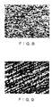
- a liquid crystal cell was prepared and evaluated in the same manner as in Experimental Example 7 except that the polyimide A alignment film for the first substrate was not rubbed. As a result, the cell showed poor homogeneity in smectic layer normal direction as shown in Figure 8 (a polarizing microscopic photograph at a magnification of 250). Further, light leakage in the dark state was noticeable, and only an areal percentage of 20 % could be switched.
- a liquid crystal cell was prepared and evaluated in the same manner as in Experimental Example 7 except that both substrates were prepared by coating with PVA followed by rubbing. As a result, the cell showed poor homogeneity in smectic layer normal direction as shown in Figure 9 (a polarizing microscopic photograph at a magnification of 250). Further, light leakage in the dark state was noticeable, and only an areal percentage of 30 % could be switched.
- a liquid crystal cell was prepared and evaluated in the same manner as in Experimental Example 7 except that the PVA alignment film for the second substrate was rubbed. As a result, the cell showed poor homogeneity in smectic layer normal direction as shown in Figure 10 (a polarizing microscopic photograph at a magnification of 250). Further, light leakage in the dark state was noticeable, and only an areal percentage of 20 % could be switched.
- the cell showed a good planar homogeneity in a layer normal direction as shown in Figure 11 (a polarizing microscopic photograph at a magnification of 250).
- the contrast was 50 and the response time was 45 ⁇ sec.
- a chiral smectic liquid crystal having no Ch phase is aligned with good planar homogeneity with respect to smectic layer normal direction and in a uniform alignment showing a large apparent tilt angle.
- a chiral smectic liquid crystal device exhibiting improved display characteristics including increased brightness and contrast and improved drive characteristics with substantially no surface memory and suppressed change in threshold for switching between the two stable states.
- Figure 12 is a graph showing a temperature-dependent layer spacing-changing characteristic of the liquid crystal material FLC-A used in the above-mentioned Experimental Examples, satisfying d min /d A ⁇ 0.96.
- Figure 13 is a graph showing the liquid crystal material TKF-8616 used in Comparative Example 1, not satisfying d min /d A ⁇ 0.96.
- a chiral smectic liquid crystal device with a good planar homogeneity in a layer normal direction can be constituted by disposing a chiral smectic liquid crystal having no cholesteric phase between a pair of substrates having mutually different characters, particularly in terms of Iso - SmA phase transition temperature.
- the liquid crystal may preferably have a layer spacing-changing characteristic such that it provides a layer spacing d A at a first transition point where the layer spacing of the liquid crystal begins to decrease on temperature decrease in the vicinity of a transition temperature from SmA phase to SmC* phase and a layer spacing d min at a second transition point where the layer spacing of the liquid crystal begins to increase on further temperature decrease from the first transition point, satisfying 0.96 ⁇ d min /d A .
Claims (11)
- Flüssigkristallvorrichtung umfassend:ein Substratpaar und einen dazwischen angeordneten Flüssigkristall, wobei der Flüssigkristall eine Phasenübergangsserie ohne Ausbildung einer cholesterischen Phase aufweist und in eine bistabile chirale smektische Phase versetzt wird und das Substratpaar asymmetrischen Ausrichtungsbehandlungen unterworfen wurde;wobei der Flüssigkristall eine Schichtabstandsänderungseigenschaft aufweist, bei der ein Schichtabstand dA an einem ersten Übergangspunkt bereitgestellt wird, an dem der Schichtabstand des Flüssigkristalls bei Temperaturverringerung in der Nähe einer Übergangstemperatur von der SmA-Phase zur SmC*-Phase abzunehmen beginnt und ein Schichtabstand dmin bei einem zweiten Übergangspunkt bereitgestellt wird, an dem der Schichtabstand des Flüssigkristalls bei weiterer Temperaturverringerung vom ersten Übergangspunkt aus anzusteigen beginnt, wobei gilt 0,96 ≤ dmin/dA.
- Flüssigkristallvorrichtung nach Anspruch 1, umfassend ein Substratpaar mit einer jeweils darauf vorgesehenen transparenten Elektrode und einem zwischen dem Substraten angeordneten Flüssigkristall,wobei der Flüssigkristall keine cholesterische Phase aufweist unddas Elektrodenpaar mit einer Vorrichtung zur Bereitstellung unterschiedlicher Phasenübergangstemperaturen von Iso- zur SmA-Phase an deren Grenzflächen zu dem Flüssigkristall ausgestattet ist.
- Flüssigkristallvorrichtung nach Anspruch 2, wobei die unterschiedlichen Phasenübergangstemperaturen von Iso- zur SmA-Phase voneinander um mindestens 0,5 °C abweichen.
- Flüssigkristallvorrichtung nach Anspruch 2 oder 3, wobei die Vorrichtung zur Bereitstellung unterschiedlicher Phasenübergangstemperatur von Iso- zur SmA-Phase durch eine Asymmetrie zwischen dem Substratpaar gegeben ist.
- Flüssigkristallvorrichtung nach Anspruch 4, wobei das Substratpaar mit gegenseitig unterschiedlichen Ausrichtungsfilmen versehen ist.
- Flüssigkristallvorrichtung nach Anspruch 5, wobei die gegenseitig unterschiedlichen Ausrichtungsfilme unterschiedliche Vortiltwinkel schaffen.
- Flüssigkristallvorrichtung nach Anspruch 1, umfassend ein Substratpaar mit einer jeweils darauf vorgesehenen transparenten Elektrode und einem zwischen den Substraten angeordneten Flüssigkristall,wobei der Flüssigkristall keine cholesterische Phase aufweist undein Substrat des Substratpaars mit einem Ausrichtungsfilm zur uniaxialen Ausrichtung des Flüssigkristalls versehen ist, wobei der Ausrichtungsfilm einen Glasübergangspunkt von wenigstens 200 °C besitzt.
- Flüssigkristallvorrichtung nach Anspruch 1, umfassend ein Substratpaar mit einer jeweils darauf vorgesehenen transparenten Elektrode und einem zwischen dem Substraten angeordneten Flüssigkristall,wobei der Flüssigkristall keine cholesterische Phase besitzt, undein Substrat des Substratpaars mit einem Ausrichtungsfilm zur uniaxialen Ausrichtung des Flüssigkristalls versehen ist, wobei der Ausrichtungsfilm ein Polyimid umfaßt.
- Flüssigkristallvorrichtung nach Anspruch 1, umfassend ein Substratpaar mit einer jeweils darauf vorgesehenen transparenten Elektrode und einem zwischen den Substraten angeordneten Flüssigkristall,wobei der Flüssigkristall keine cholesterische Phase besitzt, undein Substrat des Substratpaars mit einem uniaxialen Ausrichtungsfilm mit einem Glasübergangspunkt von wenigstens 200 °C versehen ist und das andere Substrat des Substratpaars mit einem Ausrichtungsfilm versehen ist, der für sich genommenen eine Zufallsausrichtung des Flüssigkristalls vorsehen würde.
- Flüssigkristallvorrichtung nach Anspruch 1, umfassend ein Substratpaar mit einer jeweils darauf vorgesehenen transparenten Elektrode und einem zwischen den Substraten angeordneten Flüssigkristall,wobei der Flüssigkristall keine cholesterische Phase besitzt, undein Substrat des Substratpaars mit einem uniaxialen Ausrichtungsfilm versehen ist, der ein Polyimid umfaßt und das andere Substrat des Substratpaars mit einem Ausrichtungsfilm versehen ist, der für sich genommen eine Zufallsausrichtung des Flüssigkristalls vorsehen würde.
- Flüssigkristallvorrichtung nach einem der vorhergehenden Ansprüche, wobei für dmin und dA gilt 0,99 ≤ dmin/ dA.
Applications Claiming Priority (4)
| Application Number | Priority Date | Filing Date | Title |
|---|---|---|---|
| JP21226493 | 1993-08-03 | ||
| JP21226593 | 1993-08-03 | ||
| JP212265/93 | 1993-08-03 | ||
| JP212264/93 | 1993-08-03 |
Publications (2)
| Publication Number | Publication Date |
|---|---|
| EP0637622A1 EP0637622A1 (de) | 1995-02-08 |
| EP0637622B1 true EP0637622B1 (de) | 1998-06-10 |
Family
ID=26519109
Family Applications (1)
| Application Number | Title | Priority Date | Filing Date |
|---|---|---|---|
| EP94112050A Expired - Lifetime EP0637622B1 (de) | 1993-08-03 | 1994-08-02 | Flüssigkristallvorrichtung |
Country Status (5)
| Country | Link |
|---|---|
| US (1) | US5825447A (de) |
| EP (1) | EP0637622B1 (de) |
| JP (1) | JP3179976B2 (de) |
| KR (1) | KR0153395B1 (de) |
| DE (1) | DE69410890T2 (de) |
Families Citing this family (14)
| Publication number | Priority date | Publication date | Assignee | Title |
|---|---|---|---|---|
| US5933128A (en) * | 1995-05-17 | 1999-08-03 | Canon Kabushiki Kaisha | Chiral smectic liquid crystal apparatus and driving method therefor |
| JPH09113938A (ja) * | 1995-10-13 | 1997-05-02 | Sony Corp | 液晶光学素子 |
| US5932136A (en) * | 1995-10-20 | 1999-08-03 | Canon Kabushiki Kaisha | Liquid crystal device and liquid crystal apparatus |
| JP3192593B2 (ja) * | 1996-07-22 | 2001-07-30 | キヤノン株式会社 | 液晶素子 |
| US6233027B1 (en) * | 1997-01-07 | 2001-05-15 | Canon Kabushiki Kaisha | Liquid crystal device and process for production thereof |
| US6195147B1 (en) * | 1997-08-01 | 2001-02-27 | Canon Kabushiki Kaisha | Liquid crystal substrate with optical modulation region having different alignment control forces |
| JP3472189B2 (ja) * | 1999-04-08 | 2003-12-02 | キヤノン株式会社 | キャリア輸送素子及び発光素子 |
| US6128064A (en) * | 1999-07-14 | 2000-10-03 | Canon Kabushiki Kaisha | Liquid crystal device and liquid crystal display apparatus |
| JP3667215B2 (ja) * | 1999-08-31 | 2005-07-06 | キヤノン株式会社 | 単結晶性薄膜およびその製造方法 |
| GB9928126D0 (en) * | 1999-11-30 | 2000-01-26 | Secr Defence | Bistable nematic liquid crystal device |
| JP2002201473A (ja) | 2000-10-25 | 2002-07-19 | Canon Inc | スメクチック高分子液晶及びその製造方法、これを用いた液晶素子 |
| JP4535114B2 (ja) | 2007-10-26 | 2010-09-01 | ソニー株式会社 | 撮像装置および撮像方法、表示制御装置および表示制御方法、並びに、プログラム |
| US10690986B2 (en) | 2017-09-13 | 2020-06-23 | Apple Inc. | Electronic devices having electrically adjustable optical shutters |
| KR200487712Y1 (ko) | 2018-06-19 | 2018-10-24 | 김주원 | 수술용 쉐이버 |
Family Cites Families (9)
| Publication number | Priority date | Publication date | Assignee | Title |
|---|---|---|---|---|
| US4367924A (en) * | 1980-01-08 | 1983-01-11 | Clark Noel A | Chiral smectic C or H liquid crystal electro-optical device |
| US4813767A (en) * | 1980-01-08 | 1989-03-21 | Clark Noel A | Surface stabilized ferroelectric liquid crystal devices |
| US4840463A (en) * | 1987-08-19 | 1989-06-20 | Clark Noel A | Surface stabilized ferroelectric liquid crystal devices |
| US4563059A (en) * | 1983-01-10 | 1986-01-07 | Clark Noel A | Surface stabilized ferroelectric liquid crystal devices |
| DE3373193D1 (en) * | 1983-01-06 | 1987-10-01 | Chisso Corp | Liquid crystalline compounds and mixtures thereof |
| JPS61249019A (ja) * | 1985-04-26 | 1986-11-06 | Canon Inc | 液晶素子 |
| JPS626225A (ja) * | 1985-07-02 | 1987-01-13 | Semiconductor Energy Lab Co Ltd | 液晶表示装置 |
| DE3856314T2 (de) * | 1987-12-18 | 1999-09-23 | Canon Kk | Mesomorphische Verbindung, Flüssigkristallzusammensetzung und Flüssigkristallvorrichtung |
| US5417883A (en) * | 1994-04-11 | 1995-05-23 | Minnesota Mining And Manufacturing Company | Process for controlling layer spacing in mixtures of smectic liquid crystal compounds |
-
1994
- 1994-08-02 EP EP94112050A patent/EP0637622B1/de not_active Expired - Lifetime
- 1994-08-02 DE DE69410890T patent/DE69410890T2/de not_active Expired - Fee Related
- 1994-08-03 KR KR1019940019174A patent/KR0153395B1/ko not_active IP Right Cessation
- 1994-08-03 JP JP20283394A patent/JP3179976B2/ja not_active Expired - Fee Related
-
1996
- 1996-06-19 US US08/666,916 patent/US5825447A/en not_active Expired - Fee Related
Also Published As
| Publication number | Publication date |
|---|---|
| EP0637622A1 (de) | 1995-02-08 |
| KR0153395B1 (ko) | 1998-11-16 |
| DE69410890T2 (de) | 1998-12-17 |
| JPH0798458A (ja) | 1995-04-11 |
| JP3179976B2 (ja) | 2001-06-25 |
| US5825447A (en) | 1998-10-20 |
| DE69410890D1 (de) | 1998-07-16 |
Similar Documents
| Publication | Publication Date | Title |
|---|---|---|
| US4783148A (en) | Ferroelectric liquid crystal device | |
| EP0548548B1 (de) | Flüssigkristallzusammensetzung, Flüssigkristallvorrichtung und Anzeigevorrichtung | |
| EP0553727B1 (de) | Verfahren zur Behandlung einer chiralen smektischen Flüssigkristallvorrichtung | |
| EP0637622B1 (de) | Flüssigkristallvorrichtung | |
| US5746939A (en) | Liquid crystal device | |
| EP0539992B1 (de) | Flüssigkristall-Anzeigevorrichtung | |
| US5657141A (en) | Liquid crystal device | |
| US5583682A (en) | Liquid crystal device for gradational display | |
| EP0571955B1 (de) | Flüssigkristallvorrichtung und -apparat | |
| JP2952122B2 (ja) | 液晶素子、及びこれを用いた表示装置 | |
| EP0539991B1 (de) | Flüssigkristallvorrichtung und Anzeigevorrichtung | |
| EP0647695B1 (de) | Flüssigkristallzusammensetzung, Flüssigkristallvorrichtung und diese verwendende Vorrichtung | |
| US5798056A (en) | Aligning method of liquid crystal, production process of liquid crystal device, and liquid crystal device | |
| EP0725124B1 (de) | Flüssigkristallzusammensetzung, Flüssigkristallvorrichtung und Flüssigkristallapparat | |
| EP0227419B1 (de) | Ferroelektrische Flüssigkristall-Mischung und deren Verwendung in einem optischen Modulationselement | |
| EP0725123B1 (de) | Flüssigkristallzusammensetzung, Flüssigkristallvorrichtung und Flüssigkristallapparat | |
| EP0725122B1 (de) | Flüssigkristallzusammensetzung, Flüssigkristallvorrichtung und Flüssigkristallapparat | |
| JP2547974B2 (ja) | スメクチック液晶デバイスおよびその製造方法 | |
| JP2942094B2 (ja) | 液晶組成物、液晶素子および液晶装置 | |
| JP3416374B2 (ja) | 液晶の配向処理方法、液晶素子の製造方法、及び液晶素子 | |
| JPH05323255A (ja) | 液晶組成物およびこれを用いる液晶素子 | |
| JP3221539B2 (ja) | 液晶素子及びこれらを使用した液晶装置並びに液晶表示装置 | |
| JP3585183B2 (ja) | 液晶組成物、それを有する液晶素子及びそれらを有する液晶装置 | |
| JP2663082B2 (ja) | 液晶素子 | |
| JP3585186B2 (ja) | 液晶組成物、それを有する液晶素子及びそれらを有する液晶装置 |
Legal Events
| Date | Code | Title | Description |
|---|---|---|---|
| PUAI | Public reference made under article 153(3) epc to a published international application that has entered the european phase |
Free format text: ORIGINAL CODE: 0009012 |
|
| 17P | Request for examination filed |
Effective date: 19940802 |
|
| AK | Designated contracting states |
Kind code of ref document: A1 Designated state(s): CH DE ES FR GB IT LI NL SE |
|
| 17Q | First examination report despatched |
Effective date: 19960314 |
|
| GRAG | Despatch of communication of intention to grant |
Free format text: ORIGINAL CODE: EPIDOS AGRA |
|
| GRAG | Despatch of communication of intention to grant |
Free format text: ORIGINAL CODE: EPIDOS AGRA |
|
| GRAH | Despatch of communication of intention to grant a patent |
Free format text: ORIGINAL CODE: EPIDOS IGRA |
|
| GRAH | Despatch of communication of intention to grant a patent |
Free format text: ORIGINAL CODE: EPIDOS IGRA |
|
| GRAA | (expected) grant |
Free format text: ORIGINAL CODE: 0009210 |
|
| AK | Designated contracting states |
Kind code of ref document: B1 Designated state(s): CH DE ES FR GB IT LI NL SE |
|
| PG25 | Lapsed in a contracting state [announced via postgrant information from national office to epo] |
Ref country code: NL Free format text: LAPSE BECAUSE OF FAILURE TO SUBMIT A TRANSLATION OF THE DESCRIPTION OR TO PAY THE FEE WITHIN THE PRESCRIBED TIME-LIMIT Effective date: 19980610 Ref country code: LI Free format text: LAPSE BECAUSE OF FAILURE TO SUBMIT A TRANSLATION OF THE DESCRIPTION OR TO PAY THE FEE WITHIN THE PRESCRIBED TIME-LIMIT Effective date: 19980610 Ref country code: IT Free format text: LAPSE BECAUSE OF FAILURE TO SUBMIT A TRANSLATION OF THE DESCRIPTION OR TO PAY THE FEE WITHIN THE PRESCRIBED TIME-LIMIT;WARNING: LAPSES OF ITALIAN PATENTS WITH EFFECTIVE DATE BEFORE 2007 MAY HAVE OCCURRED AT ANY TIME BEFORE 2007. THE CORRECT EFFECTIVE DATE MAY BE DIFFERENT FROM THE ONE RECORDED. Effective date: 19980610 Ref country code: ES Free format text: THE PATENT HAS BEEN ANNULLED BY A DECISION OF A NATIONAL AUTHORITY Effective date: 19980610 Ref country code: CH Free format text: LAPSE BECAUSE OF FAILURE TO SUBMIT A TRANSLATION OF THE DESCRIPTION OR TO PAY THE FEE WITHIN THE PRESCRIBED TIME-LIMIT Effective date: 19980610 |
|
| REG | Reference to a national code |
Ref country code: CH Ref legal event code: EP |
|
| REF | Corresponds to: |
Ref document number: 69410890 Country of ref document: DE Date of ref document: 19980716 |
|
| ET | Fr: translation filed | ||
| PG25 | Lapsed in a contracting state [announced via postgrant information from national office to epo] |
Ref country code: SE Free format text: LAPSE BECAUSE OF FAILURE TO SUBMIT A TRANSLATION OF THE DESCRIPTION OR TO PAY THE FEE WITHIN THE PRESCRIBED TIME-LIMIT Effective date: 19980910 |
|
| NLV1 | Nl: lapsed or annulled due to failure to fulfill the requirements of art. 29p and 29m of the patents act | ||
| REG | Reference to a national code |
Ref country code: CH Ref legal event code: PL |
|
| PLBE | No opposition filed within time limit |
Free format text: ORIGINAL CODE: 0009261 |
|
| STAA | Information on the status of an ep patent application or granted ep patent |
Free format text: STATUS: NO OPPOSITION FILED WITHIN TIME LIMIT |
|
| 26N | No opposition filed | ||
| REG | Reference to a national code |
Ref country code: GB Ref legal event code: IF02 |
|
| PGFP | Annual fee paid to national office [announced via postgrant information from national office to epo] |
Ref country code: GB Payment date: 20050727 Year of fee payment: 12 |
|
| PGFP | Annual fee paid to national office [announced via postgrant information from national office to epo] |
Ref country code: DE Payment date: 20050728 Year of fee payment: 12 |
|
| PGFP | Annual fee paid to national office [announced via postgrant information from national office to epo] |
Ref country code: FR Payment date: 20050809 Year of fee payment: 12 |
|
| PG25 | Lapsed in a contracting state [announced via postgrant information from national office to epo] |
Ref country code: DE Free format text: LAPSE BECAUSE OF NON-PAYMENT OF DUE FEES Effective date: 20070301 |
|
| GBPC | Gb: european patent ceased through non-payment of renewal fee |
Effective date: 20060802 |
|
| REG | Reference to a national code |
Ref country code: FR Ref legal event code: ST Effective date: 20070430 |
|
| PG25 | Lapsed in a contracting state [announced via postgrant information from national office to epo] |
Ref country code: GB Free format text: LAPSE BECAUSE OF NON-PAYMENT OF DUE FEES Effective date: 20060802 |
|
| PG25 | Lapsed in a contracting state [announced via postgrant information from national office to epo] |
Ref country code: FR Free format text: LAPSE BECAUSE OF NON-PAYMENT OF DUE FEES Effective date: 20060831 |