EP0632504A2 - Halbleiteranordnung mit BeTe-ZnSe Kontakt auf II-VI Halbleiter mit graduellem Energiebandabstand - Google Patents
Halbleiteranordnung mit BeTe-ZnSe Kontakt auf II-VI Halbleiter mit graduellem Energiebandabstand Download PDFInfo
- Publication number
- EP0632504A2 EP0632504A2 EP94201871A EP94201871A EP0632504A2 EP 0632504 A2 EP0632504 A2 EP 0632504A2 EP 94201871 A EP94201871 A EP 94201871A EP 94201871 A EP94201871 A EP 94201871A EP 0632504 A2 EP0632504 A2 EP 0632504A2
- Authority
- EP
- European Patent Office
- Prior art keywords
- semiconductor
- layer
- bete
- znse
- semiconductor layer
- Prior art date
- Legal status (The legal status is an assumption and is not a legal conclusion. Google has not performed a legal analysis and makes no representation as to the accuracy of the status listed.)
- Granted
Links
- 239000004065 semiconductor Substances 0.000 title claims abstract description 65
- 229910015894 BeTe Inorganic materials 0.000 claims abstract description 62
- SBIBMFFZSBJNJF-UHFFFAOYSA-N selenium;zinc Chemical compound [Se]=[Zn] SBIBMFFZSBJNJF-UHFFFAOYSA-N 0.000 claims abstract description 53
- 239000000203 mixture Substances 0.000 claims abstract description 16
- 239000000463 material Substances 0.000 claims abstract description 12
- 229910052751 metal Inorganic materials 0.000 claims abstract description 9
- 239000002184 metal Substances 0.000 claims abstract description 9
- 239000010931 gold Substances 0.000 claims abstract description 5
- PCHJSUWPFVWCPO-UHFFFAOYSA-N gold Chemical compound [Au] PCHJSUWPFVWCPO-UHFFFAOYSA-N 0.000 claims abstract description 4
- 229910052737 gold Inorganic materials 0.000 claims abstract description 4
- 239000000758 substrate Substances 0.000 claims description 17
- 238000005253 cladding Methods 0.000 claims description 9
- 229910052738 indium Inorganic materials 0.000 claims description 2
- APFVFJFRJDLVQX-UHFFFAOYSA-N indium atom Chemical compound [In] APFVFJFRJDLVQX-UHFFFAOYSA-N 0.000 claims description 2
- BASFCYQUMIYNBI-UHFFFAOYSA-N platinum Chemical compound [Pt] BASFCYQUMIYNBI-UHFFFAOYSA-N 0.000 claims 2
- 229910052697 platinum Inorganic materials 0.000 claims 1
- 238000005204 segregation Methods 0.000 abstract description 3
- 239000010410 layer Substances 0.000 description 87
- 239000011701 zinc Substances 0.000 description 42
- 229910001218 Gallium arsenide Inorganic materials 0.000 description 16
- 230000004888 barrier function Effects 0.000 description 7
- 238000010586 diagram Methods 0.000 description 7
- 239000000370 acceptor Substances 0.000 description 6
- 238000000034 method Methods 0.000 description 6
- 238000001451 molecular beam epitaxy Methods 0.000 description 6
- 229910007709 ZnTe Inorganic materials 0.000 description 5
- 150000001875 compounds Chemical class 0.000 description 5
- 230000003287 optical effect Effects 0.000 description 3
- 230000015572 biosynthetic process Effects 0.000 description 2
- 229910052793 cadmium Inorganic materials 0.000 description 2
- BDOSMKKIYDKNTQ-UHFFFAOYSA-N cadmium atom Chemical compound [Cd] BDOSMKKIYDKNTQ-UHFFFAOYSA-N 0.000 description 2
- 230000001627 detrimental effect Effects 0.000 description 2
- 239000002019 doping agent Substances 0.000 description 2
- 230000000694 effects Effects 0.000 description 2
- 238000002360 preparation method Methods 0.000 description 2
- 239000002356 single layer Substances 0.000 description 2
- 239000000243 solution Substances 0.000 description 2
- 229910052725 zinc Inorganic materials 0.000 description 2
- 102000010970 Connexin Human genes 0.000 description 1
- 108050001175 Connexin Proteins 0.000 description 1
- 239000004642 Polyimide Substances 0.000 description 1
- HCHKCACWOHOZIP-UHFFFAOYSA-N Zinc Chemical compound [Zn] HCHKCACWOHOZIP-UHFFFAOYSA-N 0.000 description 1
- 230000009471 action Effects 0.000 description 1
- 238000013459 approach Methods 0.000 description 1
- 238000004364 calculation method Methods 0.000 description 1
- 230000008859 change Effects 0.000 description 1
- 238000000576 coating method Methods 0.000 description 1
- 239000013078 crystal Substances 0.000 description 1
- 238000005516 engineering process Methods 0.000 description 1
- 210000003976 gap junction Anatomy 0.000 description 1
- 230000005525 hole transport Effects 0.000 description 1
- 238000002347 injection Methods 0.000 description 1
- 239000007924 injection Substances 0.000 description 1
- 239000012212 insulator Substances 0.000 description 1
- 238000012886 linear function Methods 0.000 description 1
- 238000004519 manufacturing process Methods 0.000 description 1
- 238000005259 measurement Methods 0.000 description 1
- 238000012986 modification Methods 0.000 description 1
- 230000004048 modification Effects 0.000 description 1
- 150000002831 nitrogen free-radicals Chemical class 0.000 description 1
- 239000002574 poison Substances 0.000 description 1
- 231100000614 poison Toxicity 0.000 description 1
- 229920001721 polyimide Polymers 0.000 description 1
- 238000012545 processing Methods 0.000 description 1
- 238000012887 quadratic function Methods 0.000 description 1
- 230000009467 reduction Effects 0.000 description 1
- 229910052950 sphalerite Inorganic materials 0.000 description 1
- 230000000638 stimulation Effects 0.000 description 1
- 238000003786 synthesis reaction Methods 0.000 description 1
- 239000011592 zinc chloride Substances 0.000 description 1
- 235000005074 zinc chloride Nutrition 0.000 description 1
- JIAARYAFYJHUJI-UHFFFAOYSA-L zinc dichloride Chemical compound [Cl-].[Cl-].[Zn+2] JIAARYAFYJHUJI-UHFFFAOYSA-L 0.000 description 1
- 229910052984 zinc sulfide Inorganic materials 0.000 description 1
Images


Classifications
-
- B—PERFORMING OPERATIONS; TRANSPORTING
- B82—NANOTECHNOLOGY
- B82Y—SPECIFIC USES OR APPLICATIONS OF NANOSTRUCTURES; MEASUREMENT OR ANALYSIS OF NANOSTRUCTURES; MANUFACTURE OR TREATMENT OF NANOSTRUCTURES
- B82Y20/00—Nanooptics, e.g. quantum optics or photonic crystals
-
- H—ELECTRICITY
- H01—ELECTRIC ELEMENTS
- H01S—DEVICES USING THE PROCESS OF LIGHT AMPLIFICATION BY STIMULATED EMISSION OF RADIATION [LASER] TO AMPLIFY OR GENERATE LIGHT; DEVICES USING STIMULATED EMISSION OF ELECTROMAGNETIC RADIATION IN WAVE RANGES OTHER THAN OPTICAL
- H01S5/00—Semiconductor lasers
- H01S5/04—Processes or apparatus for excitation, e.g. pumping, e.g. by electron beams
- H01S5/042—Electrical excitation ; Circuits therefor
- H01S5/0421—Electrical excitation ; Circuits therefor characterised by the semiconducting contacting layers
-
- H—ELECTRICITY
- H01—ELECTRIC ELEMENTS
- H01S—DEVICES USING THE PROCESS OF LIGHT AMPLIFICATION BY STIMULATED EMISSION OF RADIATION [LASER] TO AMPLIFY OR GENERATE LIGHT; DEVICES USING STIMULATED EMISSION OF ELECTROMAGNETIC RADIATION IN WAVE RANGES OTHER THAN OPTICAL
- H01S5/00—Semiconductor lasers
- H01S5/30—Structure or shape of the active region; Materials used for the active region
- H01S5/32—Structure or shape of the active region; Materials used for the active region comprising PN junctions, e.g. hetero- or double- heterostructures
- H01S5/327—Structure or shape of the active region; Materials used for the active region comprising PN junctions, e.g. hetero- or double- heterostructures in AIIBVI compounds, e.g. ZnCdSe-laser
-
- H—ELECTRICITY
- H10—SEMICONDUCTOR DEVICES; ELECTRIC SOLID-STATE DEVICES NOT OTHERWISE PROVIDED FOR
- H10D—INORGANIC ELECTRIC SEMICONDUCTOR DEVICES
- H10D62/00—Semiconductor bodies, or regions thereof, of devices having potential barriers
- H10D62/80—Semiconductor bodies, or regions thereof, of devices having potential barriers characterised by the materials
- H10D62/82—Heterojunctions
- H10D62/826—Heterojunctions comprising only Group II-VI materials heterojunctions, e.g. CdTe/HgTe heterojunctions
-
- H—ELECTRICITY
- H10—SEMICONDUCTOR DEVICES; ELECTRIC SOLID-STATE DEVICES NOT OTHERWISE PROVIDED FOR
- H10D—INORGANIC ELECTRIC SEMICONDUCTOR DEVICES
- H10D64/00—Electrodes of devices having potential barriers
- H10D64/60—Electrodes characterised by their materials
- H10D64/62—Electrodes ohmically coupled to a semiconductor
-
- H—ELECTRICITY
- H01—ELECTRIC ELEMENTS
- H01S—DEVICES USING THE PROCESS OF LIGHT AMPLIFICATION BY STIMULATED EMISSION OF RADIATION [LASER] TO AMPLIFY OR GENERATE LIGHT; DEVICES USING STIMULATED EMISSION OF ELECTROMAGNETIC RADIATION IN WAVE RANGES OTHER THAN OPTICAL
- H01S5/00—Semiconductor lasers
- H01S5/30—Structure or shape of the active region; Materials used for the active region
- H01S5/34—Structure or shape of the active region; Materials used for the active region comprising quantum well or superlattice structures, e.g. single quantum well [SQW] lasers, multiple quantum well [MQW] lasers or graded index separate confinement heterostructure [GRINSCH] lasers
- H01S5/347—Structure or shape of the active region; Materials used for the active region comprising quantum well or superlattice structures, e.g. single quantum well [SQW] lasers, multiple quantum well [MQW] lasers or graded index separate confinement heterostructure [GRINSCH] lasers in AIIBVI compounds, e.g. ZnCdSe- laser
Definitions
- the present invention relates to semiconductor devices, in particular to diode lasers comprising Group II-IV compound semiconductors.
- ZnSe:N contact layers by lowering the substrate temperature during molecular beam epitaxy growth to 150°C, and using a cracked Se source (J. Qui et al, Proceedings of VII MBE Conference Schwabisch Gemund, Germany, Aug. 24-28,1992); a ZnSe/ZnTe multilayer structure used for a contact layer to achieve a graded band gap effect from p-ZnSe to p-ZnTe (Y. Fan et al, Appl. Phys. Lett.
- ZnTe-ZnSe layers have a higher refractive index than the active region formed by ZnSe or ZnCd x Se 1-x layers, which has a detrimental effect on the optical confinement in the active region of the laser.
- an extra-thick p-cladding layer would be required which further complicates matters since it is likely to increase the voltage threshold for laser emission.
- An object of the present invention is to provide a Semiconductors device in particular a Semiconductor diodelaser, with II-VI layers, e.g. ZnSe-based layers, that are free of the problems met heretofore by prior art structures.
- Another object of the invention is to provide devices with an ohmic contact to ZnSe-based layers by a method in which the valence band affinity of the semiconductor near the surface is reduced by use of a graded gap semiconductor layer.
- Yet another object is to provide diode lasers derived from such Ohmic contacts and most preferably lasers of the blue-green type.
- BeTe is utilized in a graded band gap layer for Ohmic contact to p-type ZnSe, based semiconductors. Due to the close lattice match to GaAs and ZnSe and grown character, Be x Zn 1-x Te y Se 1-y graded band gap layers are ideal for Ohmic contact to p-type ZnSe based and other II-VI compound semiconductors. It is to be noted that a BeTe layer is known from JP-4-63479. According to this prior art docoument, the BeTe layer acts as an injection layer for a light-emitting layer.
- the conductivity type of the BeTe layer has to be opposite to the conductivity type of the light-emitting layer and a graded composition of the BeTe layer serves no purpose.
- a graded composition of the BeTe layer serves no purpose.
- Such contacts such as Be x Zn 1-x Te x Se 1-x wherein x is a number selected from the range of 0 to 1.
- the compositions of the invention will be described with reference to the composition Be x Zn 1-x Te x Se 1-x .
- BeTe-ZnSe graded gap semiconductor layers are provided for application as ohmic contacts to p- type ZnSe, ZnS x Se 1-x , Zn 1-x Cd x S, Zn 1-x Cd x S y Se 1-y , Zn 1-x Mg x S y Se 1-y (wherein x and y are a number selected from 0 to 1, and other II-VI compound semiconductors used in lasers grown on GaAs substrates. Due to the close lattice match to GaAs substrate, (BeTe) x (ZnSe) 1-x contacts allow for the entire device structure to be grown within the pseudomorphic limit.
- the band gap energy of BeTe is higher than ZnSe
- the refractive index of BeTe is expected to be lower than ZnSe or ZnCd x Se 1-x , and optical confinement around an active region in a blue or blue-green laser will not be affected by these contacts.
- the invention uses BeTe to form a compositional grading to ZnSe or other II - VI compound semiconductor lattice matched to GaAs.
- This lattice matching may prove to be critical for implementation onto room temperature operative diode lasers.
- the BeTe - ZnSe graded composition ohmic contacts are believed to be a practical and necessary solution for blue lasers grown on GaAs substrates.
- a large barrier in valence band at the BeTe/ZnSe heterojunction would suppress transport of holes fron BeTe to ZnSe.
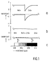
- a large valence band offset in abrupt BeTe/ZnSe heterojunction can almost entirely be removed if linearly graded heterojunction is used, as shown in Fig. 1b in which grading takes place from 200 to 1000 ⁇ which is indicated by arrows.
- an epitaxial growth of BeTe-ZnSe graded layer is preferably done by digital technique in which layers of the graded components are alternately grown in predetermined thicknesses and numbers as represented by (BeTe) x (ZnSe) 1-x .
- the graded gap junction is divided into 20 segments, each 40A wide.
- the second segment contains 2 ⁇ of p-ZnSe and 38 ⁇ of p-BeTe;
- the third segment has 4 ⁇ of p-ZnSe and 36 ⁇ of p-BeTe, etc.
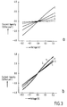
- Figs. 2 and 3 there are illustrated the energy band diagram for linear (solid line) and quadratic (dashed line) Be x Zn 1-x Te x Se 1-x graded junctions of several widths.
- the cusps in the valence band appearing in linearly graded junction near the edges of the linearly graded Be x Zn 1-x Te x Se 1-x junction at l1 and l2 act on a hole transport as a trap and a barrier, respectively, i.e. the cusps act as a well and a barrier for mobile holes, respectively.
- the detrimental influence of the barrier around l2 on the contact resistance is more significant, and can be reduced by introducing quadratic grading through the entire Be x Zn 1-x Te x Se 1-x layer, as illustrated in Fig. 2. This becomes quite apparent from the comparison of the calculated current-voltage characteristics of the quadratically and linearly graded contacts shown in Fig. 3 by curves 1 and 5.
- the continuous lines correspond to linearly graded p-Be x Zn 1-x Te x Se 1-x junctions doped uniformly at 1 and 2x1018 cm ⁇ 3 (curves 1 and 2 ,respectively), and linearly doped from 1018 cm ⁇ 3 at l2, to 5 and 10x10'8 cm ⁇ 3 at l1 (curves 3 and 4, respectively).
- the dotted line in Fig. 3 (curve 5) corresponds to quadratically graded Be x Zn 1-x Te x Se 1-x layers doped uniformly with acceptors at 1x1018 cm ⁇ 3 level.
- an increase in doping level of p-ZnSe to 2x1018 cm ⁇ 3 lowers the contact resistivity of Be x Zn 1-x Te x Se 1-x linearly graded layers more significantly than an increase in doping in p-BeTe, even at as high a level as 1x1019cm ⁇ 3. Therefore, if an upper limit of p-ZnSe doping is selected to be 1x1018 cm ⁇ 3, the junction width, w J , of the Be x Zn 1-x Te x Se 1-x layer should be increased.
- the contact resistance of the linearly graded p-Be x Zn 1-x Te x Se 1-x layers as a function of the junction width w j , for uniform doping at 1x1018 cm ⁇ 3 is illustrated in Fig. 4.
- the structure included 200 ⁇ p-BeTe and 300-900 ⁇ p-Be x Zn 1-x Te x Se 1-x where the total thickness will still allow for pseudomorphic growth of these layers on GaAs substrate and for the production of blue laser structures entirely lattice matched to GaAs substrate.
- the graded Be x Zn 1-x Te x Se 1-x layer may be utilized to fabricate blue-green lasers according to methods such as, for example that described in Gaines et al, Appl. Phys. Lett. ,62(20), pp.2462 (1993) and in Gaines et al, copending U.S. Application Ser.No. 07/997,988 filed December.
- Particularly preferred is a structure as illustrated in Fig.5 which illustrates a laser diode 10 which may be generally be grown by molecular beam epitaxy (MBE) on a GaAs substrate 20 and includes an ohmic contact layer 16 which comprises a graded band gap Be x Zn 1-x Te x Se 1-x composition of the invention.
- MBE molecular beam epitaxy
- a bottom waveguide cladding layer 22 of ZnS x Se 1-x which by its doping is n-type.
- Grown atop cladding layer 22 is a layer of ZnSe 24 which forms the bottom half of the waveguide.
- Grown on layer 24 is an active region 26 consisting of three undoped Cd u Zn 1-u Se quantum wells separated by two undoped ZnSe spacer regions.
- Grown on active region 26 is a p-ZnSe guiding layer 28.
- Grown on layer 28 is a p- ZnS z Se 1-z top cladding layer 30.
- an ohmic contact layer 16 which comprises a graded band gap Be x Zn 1-x Te x Se 1-x part 17 and a BeTe part 18 according to the invention.
- a polyimide insulator layer 32 with openings 33 is applied and contacts to part 18 of the contact layer 16 and the GaAs substrate were made with gold layers 34, 35.
- Source materials may be selected from those well known in the art and are preferably Zn, Se, Cd, and ZnS.
- the p- and n- type dopants may be N, excited by a plasma source, and Cl (from ZnCl2), respectively.
- Doping levels and processing may be as described in said copending application, i.e. the doping levels for the layers 22, 24, 28 and 30 are approximately 1x10¹⁸, 3x10¹⁷, and 2x1017 cm ⁇ 3, respectively.
- the doping level in the p- ZnS z Se 1-z layer 30 may be 2x1017 cm ⁇ 3 and that in the graded band gap composition layer 16 may be approximately at the levels discussed above with respect to Figs. 3 and 4, i.e. doping will vary depending on the grading and the particular area of the grading, the junction width, etc, and is preferably at least 1x1018 cm ⁇ 3.
- each of the layers is grown in a manner so as to minimize the loss of light in absorbing layers and maximize the amount of light in the active region with specific thicknesses being illustrated in Fig. 5 for purposes of illustration only.
- useful devices may be made with a n-type cladding layer 22 of 2.0 microns, an guiding layers 24 and 28, including the quantum well region 26 having a thickness of about 60 ⁇ with about 110 ⁇ thick ZnSe spacers in between,has a total thickness of approximately 1 micron.
- the p-type top cladding layer 30 and the p-type graded band gap contact layer 16 have a total thickness of about 1.5 micron, the graded contact layer 16 having a thickness of approximately 400 to 800 ⁇ .
- Suitable ranges for u(cadmium) are from 0 to 1.0z from 0 to 0.1,y from 0 to 1 and x from 0 to 1, with x an y being selected to provide lattice matching to GaAs.
- facet coatings and may be applied to mirrors 36, 38 of the device.
- the cleaving of the device to its useful length, here about 500 mg provides the necessary "mirror" action to provide laser stimulation.
- the light output may be shifted towards blue by reducing the thickness of active region 26 and/or by reducing the cadmium content of this layer (u approaches 0).
- the substrate and lower layers are n-type with the upper layers being p-type.
- An analogous structure can be grown with the lower layers p-type and the upper layers n-type.
Landscapes
- Physics & Mathematics (AREA)
- Optics & Photonics (AREA)
- General Physics & Mathematics (AREA)
- Chemical & Material Sciences (AREA)
- Engineering & Computer Science (AREA)
- Nanotechnology (AREA)
- Condensed Matter Physics & Semiconductors (AREA)
- Electromagnetism (AREA)
- Biophysics (AREA)
- Crystallography & Structural Chemistry (AREA)
- Life Sciences & Earth Sciences (AREA)
- Semiconductor Lasers (AREA)
- Led Devices (AREA)
Applications Claiming Priority (2)
| Application Number | Priority Date | Filing Date | Title |
|---|---|---|---|
| US08/087,307 US5422902A (en) | 1993-07-02 | 1993-07-02 | BeTe-ZnSe graded band gap ohmic contact to p-type ZnSe semiconductors |
| US87307 | 1993-07-02 |
Publications (3)
| Publication Number | Publication Date |
|---|---|
| EP0632504A2 true EP0632504A2 (de) | 1995-01-04 |
| EP0632504A3 EP0632504A3 (de) | 1995-11-15 |
| EP0632504B1 EP0632504B1 (de) | 1997-09-10 |
Family
ID=22204390
Family Applications (1)
| Application Number | Title | Priority Date | Filing Date |
|---|---|---|---|
| EP94201871A Expired - Lifetime EP0632504B1 (de) | 1993-07-02 | 1994-06-29 | Halbleitervorrichtung mit Gradienten-Bandabstand BeTe-ZnSe ohmschem Kontakt für einen II-VI Halbleiter |
Country Status (4)
| Country | Link |
|---|---|
| US (1) | US5422902A (de) |
| EP (1) | EP0632504B1 (de) |
| JP (1) | JPH0758417A (de) |
| DE (1) | DE69405486T2 (de) |
Cited By (3)
| Publication number | Priority date | Publication date | Assignee | Title |
|---|---|---|---|---|
| EP0734071A3 (de) * | 1995-03-24 | 1998-04-15 | Sharp Kabushiki Kaisha | II-VI-Verbindungshalbleiterbauelement und dessen Herstellungsverfahren |
| WO1999003156A1 (de) * | 1997-07-09 | 1999-01-21 | Osram Opto Semiconductors Gmbh & Co. Ohg | II-VI-HALBLEITERBAUELEMENT MIT MINDESTENS EINEM ÜBERGANG VON EINER Se-ENTHALTENDEN SCHICHT AUF EINE BeTe-ENTHALTENDE SCHICHT UND VERFAHREN ZUM HERSTELLEN DES ÜBERGANGES |
| EP1622207A4 (de) * | 2003-04-23 | 2007-08-08 | Hoya Corp | Leuchtdiode |
Families Citing this family (11)
| Publication number | Priority date | Publication date | Assignee | Title |
|---|---|---|---|---|
| WO1994015369A1 (en) * | 1992-12-22 | 1994-07-07 | Research Corporation Technologies, Inc. | Group ii-vi compound semiconductor light emitting devices and an ohmic contact therefor |
| DE19542241C2 (de) * | 1995-11-13 | 2003-01-09 | Siemens Ag | Optoelektronisches Bauelement in II-VI-Halbleitermaterial |
| US5818859A (en) * | 1996-06-27 | 1998-10-06 | Minnesota Mining And Manufacturing Company | Be-containing II-VI blue-green laser diodes |
| US5841802A (en) * | 1996-08-30 | 1998-11-24 | Mcdonnell Douglas Corporation | Multiple, isolated strained quantum well semiconductor laser |
| US6090637A (en) * | 1997-02-13 | 2000-07-18 | 3M Innovative Properties Company | Fabrication of II-VI semiconductor device with BeTe buffer layer |
| US5767534A (en) * | 1997-02-24 | 1998-06-16 | Minnesota Mining And Manufacturing Company | Passivation capping layer for ohmic contact in II-VI semiconductor light transducing device |
| DE19729186A1 (de) * | 1997-07-08 | 1999-01-14 | Siemens Ag | Verfahren zum Herstellen eines II-VI-Halbleiter-Bauelements |
| US5963573A (en) * | 1997-08-25 | 1999-10-05 | 3M Innovative Properties Company | Light absorbing layer for II-VI semiconductor light emitting devices |
| US6087725A (en) * | 1997-09-29 | 2000-07-11 | Matsushita Electric Industrial Co., Ltd. | Low barrier ohmic contact for semiconductor light emitting device |
| US6373188B1 (en) * | 1998-12-22 | 2002-04-16 | Honeywell International Inc. | Efficient solid-state light emitting device with excited phosphors for producing a visible light output |
| DE10024924A1 (de) * | 2000-05-19 | 2001-11-29 | Osram Opto Semiconductors Gmbh | Licht emittierendes Halbleiterbauelement |
Family Cites Families (19)
| Publication number | Priority date | Publication date | Assignee | Title |
|---|---|---|---|---|
| US3933538A (en) * | 1972-01-18 | 1976-01-20 | Sumitomo Electric Industries, Ltd. | Method and apparatus for production of liquid phase epitaxial layers of semiconductors |
| US4801984A (en) * | 1980-06-12 | 1989-01-31 | International Business Machines Corporation | Semiconductor ohmic contact |
| US5140385A (en) * | 1987-03-27 | 1992-08-18 | Misawa Co., Ltd. | Light emitting element and method of manufacture |
| US5068204A (en) * | 1987-03-27 | 1991-11-26 | Misawa Co. Ltd. | Method of manufacturing a light emitting element |
| JPH02229484A (ja) * | 1988-06-08 | 1990-09-12 | Furukawa Electric Co Ltd:The | 半導体素子 |
| JP2708183B2 (ja) * | 1988-07-21 | 1998-02-04 | シャープ株式会社 | 化合物半導体発光素子 |
| JPH0268968A (ja) * | 1988-09-02 | 1990-03-08 | Sharp Corp | 化合物半導体発光素子 |
| US5060233A (en) * | 1989-01-13 | 1991-10-22 | International Business Machines Corporation | Miniature blue-green laser source using second-harmonic generation |
| JPH0717477B2 (ja) * | 1989-03-15 | 1995-03-01 | シャープ株式会社 | 化合物半導体のエピタキシャル成長方法 |
| JP2559492B2 (ja) * | 1989-07-05 | 1996-12-04 | シャープ株式会社 | 化合物半導体発光素子の製造方法 |
| JP2588280B2 (ja) * | 1989-07-10 | 1997-03-05 | シャープ株式会社 | 化合物半導体発光素子 |
| US4949348A (en) * | 1989-08-25 | 1990-08-14 | The United States Of America As Represented By The Department Of Energy | Blue-green upconversion laser |
| JP2653901B2 (ja) * | 1990-07-02 | 1997-09-17 | シャープ株式会社 | 化合物半導体発光素子 |
| US5248631A (en) * | 1990-08-24 | 1993-09-28 | Minnesota Mining And Manufacturing Company | Doping of iib-via semiconductors during molecular beam epitaxy using neutral free radicals |
| JP2685377B2 (ja) * | 1990-11-26 | 1997-12-03 | シャープ株式会社 | 化合物半導体発光素子 |
| GB2250635B (en) * | 1990-11-26 | 1994-09-28 | Sharp Kk | Electroluminescent device of compound semiconductor and process for fabricating the same |
| US5213998A (en) * | 1991-05-15 | 1993-05-25 | Minnesota Mining And Manufacturing Company | Method for making an ohmic contact for p-type group II-VI compound semiconductors |
| WO1992021170A2 (en) * | 1991-05-15 | 1992-11-26 | Minnesota Mining And Manufacturing Company | Blue-green laser diode |
| US5162891A (en) * | 1991-07-03 | 1992-11-10 | International Business Machines Corporation | Group III-V heterostructure devices having self-aligned graded contact diffusion regions and method for fabricating same |
-
1993
- 1993-07-02 US US08/087,307 patent/US5422902A/en not_active Expired - Fee Related
-
1994
- 1994-06-29 EP EP94201871A patent/EP0632504B1/de not_active Expired - Lifetime
- 1994-06-29 DE DE69405486T patent/DE69405486T2/de not_active Expired - Fee Related
- 1994-07-01 JP JP15115594A patent/JPH0758417A/ja active Pending
Cited By (5)
| Publication number | Priority date | Publication date | Assignee | Title |
|---|---|---|---|---|
| EP0734071A3 (de) * | 1995-03-24 | 1998-04-15 | Sharp Kabushiki Kaisha | II-VI-Verbindungshalbleiterbauelement und dessen Herstellungsverfahren |
| US6033929A (en) * | 1995-03-24 | 2000-03-07 | Sharp Kabushiki Kaisha | Method for making II-VI group compound semiconductor device |
| WO1999003156A1 (de) * | 1997-07-09 | 1999-01-21 | Osram Opto Semiconductors Gmbh & Co. Ohg | II-VI-HALBLEITERBAUELEMENT MIT MINDESTENS EINEM ÜBERGANG VON EINER Se-ENTHALTENDEN SCHICHT AUF EINE BeTe-ENTHALTENDE SCHICHT UND VERFAHREN ZUM HERSTELLEN DES ÜBERGANGES |
| US6372536B1 (en) | 1997-07-09 | 2002-04-16 | Osram Opto Semiconductors & Co. Ohg | II-VI semiconductor component having at least one junction between a layer containing Se and a layer containing BeTe, and process for producing the junction |
| EP1622207A4 (de) * | 2003-04-23 | 2007-08-08 | Hoya Corp | Leuchtdiode |
Also Published As
| Publication number | Publication date |
|---|---|
| EP0632504B1 (de) | 1997-09-10 |
| DE69405486T2 (de) | 1998-03-19 |
| EP0632504A3 (de) | 1995-11-15 |
| JPH0758417A (ja) | 1995-03-03 |
| US5422902A (en) | 1995-06-06 |
| DE69405486D1 (de) | 1997-10-16 |
Similar Documents
| Publication | Publication Date | Title |
|---|---|---|
| USRE37177E1 (en) | Semiconductor laser | |
| Tanaka et al. | InGaP/InGaAlP double‐heterostructure and multiquantum‐well laser diodes grown by molecular‐beam epitaxy | |
| US5889295A (en) | Semiconductor device | |
| US6372536B1 (en) | II-VI semiconductor component having at least one junction between a layer containing Se and a layer containing BeTe, and process for producing the junction | |
| US5010374A (en) | Quantum well laser utilizing an inversion layer | |
| EP0632504B1 (de) | Halbleitervorrichtung mit Gradienten-Bandabstand BeTe-ZnSe ohmschem Kontakt für einen II-VI Halbleiter | |
| EP0215298B1 (de) | Halbleiterlaser | |
| KR100292308B1 (ko) | 반도체장치 | |
| US5475700A (en) | Laser diode with electron and hole confinement and barrier layers | |
| US5539239A (en) | Semiconductor light emitting element with II-VI and III-V compounds | |
| US6324200B1 (en) | Semiconductor laser device | |
| EP0544968A1 (de) | Auf einer strukturierten Substratoberfläche aufgewachsene Halbleiter-Laserdiode | |
| US5782996A (en) | Graded compositions of II-VI semiconductors and devices utilizing same | |
| JP3221073B2 (ja) | 発光素子 | |
| US5640409A (en) | Semiconductor laser | |
| US5572539A (en) | II-VI semiconductor laser with different guide layers | |
| EP0632554B1 (de) | Lichtemittierende Halbleitervorrichtung | |
| US20050152424A1 (en) | Low voltage defect super high efficiency diode sources | |
| JPH10504140A (ja) | イオン注入を用いてストライプ構造のii/vi半導体利得導波形注入レーザ構造を製造する方法 | |
| EP0867949B1 (de) | Lichtemittierende Halbleitervorrichtung | |
| JP3315378B2 (ja) | 半導体レーザ素子 | |
| EP0622880A2 (de) | Hetero-Grenzfläche mit reduziertem Widerstand | |
| JPH09107155A (ja) | 半導体発光素子 | |
| JP2001284728A (ja) | 半導体レーザ素子 | |
| JPH0766503A (ja) | 発光素子 |
Legal Events
| Date | Code | Title | Description |
|---|---|---|---|
| PUAI | Public reference made under article 153(3) epc to a published international application that has entered the european phase |
Free format text: ORIGINAL CODE: 0009012 |
|
| AK | Designated contracting states |
Kind code of ref document: A2 Designated state(s): DE FR GB NL |
|
| PUAL | Search report despatched |
Free format text: ORIGINAL CODE: 0009013 |
|
| AK | Designated contracting states |
Kind code of ref document: A3 Designated state(s): DE FR GB NL |
|
| RHK1 | Main classification (correction) |
Ipc: H01S 3/025 |
|
| 17P | Request for examination filed |
Effective date: 19960515 |
|
| GRAG | Despatch of communication of intention to grant |
Free format text: ORIGINAL CODE: EPIDOS AGRA |
|
| 17Q | First examination report despatched |
Effective date: 19961018 |
|
| GRAH | Despatch of communication of intention to grant a patent |
Free format text: ORIGINAL CODE: EPIDOS IGRA |
|
| GRAH | Despatch of communication of intention to grant a patent |
Free format text: ORIGINAL CODE: EPIDOS IGRA |
|
| GRAA | (expected) grant |
Free format text: ORIGINAL CODE: 0009210 |
|
| AK | Designated contracting states |
Kind code of ref document: B1 Designated state(s): DE FR GB NL |
|
| PG25 | Lapsed in a contracting state [announced via postgrant information from national office to epo] |
Ref country code: NL Free format text: LAPSE BECAUSE OF FAILURE TO SUBMIT A TRANSLATION OF THE DESCRIPTION OR TO PAY THE FEE WITHIN THE PRESCRIBED TIME-LIMIT Effective date: 19970910 |
|
| REF | Corresponds to: |
Ref document number: 69405486 Country of ref document: DE Date of ref document: 19971016 |
|
| ET | Fr: translation filed | ||
| NLV1 | Nl: lapsed or annulled due to failure to fulfill the requirements of art. 29p and 29m of the patents act | ||
| PLBE | No opposition filed within time limit |
Free format text: ORIGINAL CODE: 0009261 |
|
| STAA | Information on the status of an ep patent application or granted ep patent |
Free format text: STATUS: NO OPPOSITION FILED WITHIN TIME LIMIT |
|
| 26N | No opposition filed | ||
| REG | Reference to a national code |
Ref country code: FR Ref legal event code: CD |
|
| PGFP | Annual fee paid to national office [announced via postgrant information from national office to epo] |
Ref country code: FR Payment date: 20010625 Year of fee payment: 8 |
|
| PGFP | Annual fee paid to national office [announced via postgrant information from national office to epo] |
Ref country code: GB Payment date: 20010629 Year of fee payment: 8 |
|
| PGFP | Annual fee paid to national office [announced via postgrant information from national office to epo] |
Ref country code: DE Payment date: 20010821 Year of fee payment: 8 |
|
| REG | Reference to a national code |
Ref country code: GB Ref legal event code: IF02 |
|
| PG25 | Lapsed in a contracting state [announced via postgrant information from national office to epo] |
Ref country code: GB Free format text: LAPSE BECAUSE OF NON-PAYMENT OF DUE FEES Effective date: 20020629 |
|
| PG25 | Lapsed in a contracting state [announced via postgrant information from national office to epo] |
Ref country code: DE Free format text: LAPSE BECAUSE OF NON-PAYMENT OF DUE FEES Effective date: 20030101 |
|
| GBPC | Gb: european patent ceased through non-payment of renewal fee |
Effective date: 20020629 |
|
| PG25 | Lapsed in a contracting state [announced via postgrant information from national office to epo] |
Ref country code: FR Free format text: LAPSE BECAUSE OF NON-PAYMENT OF DUE FEES Effective date: 20030228 |
|
| REG | Reference to a national code |
Ref country code: FR Ref legal event code: ST |