EP0631330A2 - GaP-Substrat einer pur grünes licht emittierenden Vorrichtung - Google Patents
GaP-Substrat einer pur grünes licht emittierenden Vorrichtung Download PDFInfo
- Publication number
- EP0631330A2 EP0631330A2 EP94107563A EP94107563A EP0631330A2 EP 0631330 A2 EP0631330 A2 EP 0631330A2 EP 94107563 A EP94107563 A EP 94107563A EP 94107563 A EP94107563 A EP 94107563A EP 0631330 A2 EP0631330 A2 EP 0631330A2
- Authority
- EP
- European Patent Office
- Prior art keywords
- gap layer
- gap
- light emitting
- green light
- type
- Prior art date
- Legal status (The legal status is an assumption and is not a legal conclusion. Google has not performed a legal analysis and makes no representation as to the accuracy of the status listed.)
- Granted
Links
- 239000000758 substrate Substances 0.000 title claims abstract description 37
- 239000013078 crystal Substances 0.000 claims abstract description 11
- 239000012535 impurity Substances 0.000 claims description 11
- NINIDFKCEFEMDL-UHFFFAOYSA-N Sulfur Chemical compound [S] NINIDFKCEFEMDL-UHFFFAOYSA-N 0.000 claims description 9
- 229910052717 sulfur Inorganic materials 0.000 claims description 9
- 239000011593 sulfur Substances 0.000 claims description 9
- OKTJSMMVPCPJKN-UHFFFAOYSA-N Carbon Chemical compound [C] OKTJSMMVPCPJKN-UHFFFAOYSA-N 0.000 claims description 4
- 229910052799 carbon Inorganic materials 0.000 claims description 4
- 229910052710 silicon Inorganic materials 0.000 claims description 3
- 239000010703 silicon Substances 0.000 claims description 3
- 239000000243 solution Substances 0.000 description 11
- 239000000370 acceptor Substances 0.000 description 9
- 238000000034 method Methods 0.000 description 8
- 239000002019 doping agent Substances 0.000 description 5
- IJGRMHOSHXDMSA-UHFFFAOYSA-N Atomic nitrogen Chemical compound N#N IJGRMHOSHXDMSA-UHFFFAOYSA-N 0.000 description 4
- 239000012159 carrier gas Substances 0.000 description 4
- 239000007791 liquid phase Substances 0.000 description 4
- 239000004065 semiconductor Substances 0.000 description 4
- 238000002347 injection Methods 0.000 description 3
- 239000007924 injection Substances 0.000 description 3
- 238000004519 manufacturing process Methods 0.000 description 3
- 238000007796 conventional method Methods 0.000 description 2
- 239000007789 gas Substances 0.000 description 2
- 229910052757 nitrogen Inorganic materials 0.000 description 2
- 239000000969 carrier Substances 0.000 description 1
- 230000007935 neutral effect Effects 0.000 description 1
- 230000006798 recombination Effects 0.000 description 1
- 238000005215 recombination Methods 0.000 description 1
Images


Classifications
-
- H—ELECTRICITY
- H10—SEMICONDUCTOR DEVICES; ELECTRIC SOLID-STATE DEVICES NOT OTHERWISE PROVIDED FOR
- H10H—INORGANIC LIGHT-EMITTING SEMICONDUCTOR DEVICES HAVING POTENTIAL BARRIERS
- H10H20/00—Individual inorganic light-emitting semiconductor devices having potential barriers, e.g. light-emitting diodes [LED]
- H10H20/80—Constructional details
- H10H20/81—Bodies
- H10H20/822—Materials of the light-emitting regions
- H10H20/824—Materials of the light-emitting regions comprising only Group III-V materials, e.g. GaP
- H10H20/8242—Materials of the light-emitting regions comprising only Group III-V materials, e.g. GaP characterised by the dopants
Definitions
- This invention relates to a GaP pure green light emitting element substrate, and more precisely to a GaP pure green light emitting element substrate comprising a plurality of GaP layers formed on a GaP single crystal substrate, which is used to manufacture high-brightness GaP pure green light emitting elements.
- Light emitting elements such as light emitting diodes are normally obtained by layering a plurality of semiconductor layers on a semiconductor substrate to prepare a multi-layer semiconductor substrate with a pn junction, and then making it into elements for practical use.
- green light emitting diodes can be obtained by using a light emitting element substrate prepared by forming one or more layers of both n-type and p-type GaP, one after another, on an n-type GaP single crystal substrate.
- GaP is an indirect transition-type semiconductor, and therefore the brightness is very low if a pn junction is just formed. Because of this, nitrogen (N), which would function as light emitting centers, is added to the n-type GaP layer near the pn junction in order to enhance the brightness.
- N nitrogen
- a light emitting diode prepared from a GaP light emitting element substrate which has the nitrogen-added n-type GaP layer emits a yellowish-green light with a peak wavelength of about 567 nm and therefore it does not give a pure green light with a peak wavelength of about 555 nm.
- Figure 5 shows a cross-sectional structure of a GaP pure green light emitting diode which has an n-type GaP layer with a low carrier concentration (net donor concentration) formed on an n-type GaP layer with a high concentration of the impurity (electrodes are not shown).
- This type of cross-sectional structure is disclosed in Japanese unexamined patent publication (Tokkai) Sho 59-214276, for example.
- an n-type GaP layer 51, a low-carrier-concentration n-type GaP layer 52 and a p-type GaP layer 53 are formed, one after another, on an n-type GaP single crystal substrate 50, and said low-carrier-concentration n-type GaP layer 52 functions as the light emitting layer.
- the net donor concentration (n) in the low-carrier-concentration n-type GaP layer 52 is set between 5 ⁇ 1015 to 1 ⁇ 1016 atoms/cm3, substantially lower than that in the p-type GaP layer 53. This improves the injection efficiency of the holes from the p-type GaP layer 53 into the low-carrier-concentration n-type GaP layer 52, thus improving the light emitting efficiency.
- FIG. 6 shows a structure (electrodes are not shown) of a GaP pure green light emitting diode, which is disclosed in Japanese unexamined patent publication (Tokkai) Sho 57-93589.
- This GaP pure green light emitting diode has a p-type GaP layer with a lower carrier concentration (p) compared to the carrier concentration (n) in the n-type GaP layer which constitutes one side of the pn junction (said p-type GaP layer being a p-type GaP layer to which impurity as shallow donors has been added so that the net acceptor concentration is lowerd).
- an n-type GaP layer 61, a low-carrier-concentration p-type GaP layer 62 which has a carrier concentration lower than that in the n-type GaP layer 61, and a p-type GaP layer 63 are formed on an n-type GaP single crystal substrate 60, and said low-carrier-concentration p-type GaP layer 62 functions as the light emitting layer.
- the carrier concentration (N A (acceptor concentration) - N D (donor concentration)) is kept low by adding shallow donors (impurities) such as S (sulfur) in the range of the concentration N D , 1 ⁇ 1016 ⁇ N D ⁇ 3 ⁇ 1017 atoms/cm3, and the shallow donors in the low-carrier-concentration p-type GaP layer 62 become light emitting centers.
- the object of this invention is to provide a GaP pure green light emitting element substrate which allows to manufacture GaP light emitting diodes which emit pure green light at high brightness.
- This invention provides a GaP pure green light emitting element substrate comprising at least one n-type GaP layer and at least one p-type GaP layer formed on a GaP single crystal substrate, characterized by the fact that an intermediate GaP layer is formed at the pn junction portion between said n-type GaP layer and said p-type GaP layer, wherein said intermediate GaP layer has a donor concentration N D of less than 1 ⁇ 1016 atoms/cm3 and an acceptor concentration N A nearly equal to the donor concentration N D .
- the thickness of said intermediate GaP layer is preferably in the range of 3-5 micrometers.
- Said donor impurity is S (sulfur) and/or Si (silicon), for example, and said acceptor impurity is C (carbon), for example.
- the conductive type of said intermediate GaP layer can be either p-type or n-type.
- the hole injection efficiency from the p-type GaP layer to the n-type GaP layer and/or the electron injection efficiency from the n-type GaP layer to the p-type GaP layer is enhanced.
- this intermediate GaP layer is set to approximately 3-5 micrometers so that the carriers can pass through this intermediate GaP layer and then reach the n-type GaP layer and/or the p-type GaP layer, thus the radiative recombination occurs sufficiently in the n-type GaP layer with a high donor concentration and/or in the p-type GaP layer with a high acceptor concentration, resulting in enough efficient emission of pure green light.
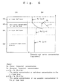
- Figure 1 shows one example of the GaP pure green light emitting element substrate of this invention.
- (A) is its cross section, and (B) shows the distribution of carrier concentration in each layer.
- Figure 2 shows the configuration of one example of the liquid phase epitaxial growth apparatus used for growing each layer of the GaP pure green light emitting substrate of this invention by means of the liquid phase epitaxial growth method.
- Figure 3 shows the growth program for growing each layer of the GaP pure green light emitting substrate of this invention by means of the liquid phase epitaxial growth method.
- Figure 4 shows the relationship between the brightness (relative value) of the GaP pure green light emitting element obtained from the GaP pure green light emitting substrate of this invention and the thickness of the intermediate GaP layer 13.
- Figure 5 shows one example of a conventional GaP pure green light emitting diode.
- A is its cross section (electrodes are not shown), and
- B) shows the distribution of carrier concentration in each layer.
- Figure 6 shows another example of a conventional GaP pure green light emitting diode.
- A is its cross section (electrodes are not shown), and
- B) shows the distribution of carrier concentration in each layer.
- Figure 1 shows a cross-sectional structure of one example of the GaP pure green light emitting element substrate of this invention and the distribution of carrier concentration in each layer.
- the structure of the GaP pure green light emitting element substrate of this example follows: as shown in Figure 1 (A), a n-type GaP buffer layer 11 to which Te and such is added as an impurity and a n-type GaP layer 12 to which S (sulfur) and such are added as impurities are formed on a n-type GaP single crystal substrate 10 to which Te and such are added as impurities, and, as the topmost layer, a p-type GaP layer 14 to which Zn and such are added as impurities is formed, wherein an intermediate GaP layer 13 with a thickness of 3-5 micrometer is formed between said n-type GaP layer 12 and p-type GaP layer 14.
- the donor concentration N D and the acceptor concentration N A are both set to be low and nearly equal to each other. That is, as shown in Figure 1 (B), the net donor concentration or the net acceptor concentration in the intermediate GaP layer 13 is approximately 1 ⁇ 1014 atoms/cm3, indicating a very weak p-type or n-type, substantially nearly neutral.
- Figure 2 shows the configuration of the liquid phase epitaxial growth apparatus used for growing each layer on the GaP single crystal substrate 10.
- a process tube 23 accommodates in it a carbon slide boat 24 which has a wafer chamber 25 containing a substrate 30 (comprising an n-type GaP buffer layer 11 already formed on an n-type GaP single crystal substrate 10).
- a solution reservoir 27 which contains a Ga solution 28 and has an opening at the bottom, is provided in such a way that it can be slid by a sliding rod 26.
- a main heater 21 to heat the area around the solution reservoir 27 and a sub heater 22 to heat the area around Zn 29 are provided.
- a carrier gas composed of a mixed gas of H2 and Ar is fed into the process tube 23 through the carrier gas supply port 31 and discharged from a gas discharge port 32.
- Figure 3 shows a growth program for growing, one after another, an n-type GaP layer 12, an intermediate GaP layer 13 and a p-type GaP layer 14 on a substrate 30 comprising an GaP buffer layer 11 formed on a GaP single crystal substrate 10. The actual growth procedure is described below.
- the GaP light emitting element substrate thus obtained is made into elements to obtain light emitting elements (light emitting diodes) which emit pure green light.
- Figure 4 shows the relationship between the thickness of the intermediate GaP layer 13 and the brightness (relative values) of the GaP pure green light emitting elements obtained from the GaP light emitting element substrate described above.
- the brightness at zero thickness of the intermediate layer corresponds to the brightness of the conventional method.
- the figure indicates that the maximum of the brightness appears when the thickness of the intermediate GaP layer 13 is approximately 4 micrometers, and the brightness is improved by 15% or more when the thickness of the intermediate GaP layer 13 is in the range of 3-5 micrometers as compared with that in the conventional method.
- this invention makes it possible to obtain GaP light emitting elements which emit pure green light at high-brightness and whose brightness is improved by as much as approximately 20% over conventional pure green light emitting elements.
Landscapes
- Led Devices (AREA)
Applications Claiming Priority (3)
| Application Number | Priority Date | Filing Date | Title |
|---|---|---|---|
| JP15416893A JP2817577B2 (ja) | 1993-05-31 | 1993-05-31 | GaP純緑色発光素子基板 |
| JP15416893 | 1993-05-31 | ||
| JP154168/93 | 1993-05-31 |
Publications (3)
| Publication Number | Publication Date |
|---|---|
| EP0631330A2 true EP0631330A2 (de) | 1994-12-28 |
| EP0631330A3 EP0631330A3 (de) | 1995-03-22 |
| EP0631330B1 EP0631330B1 (de) | 2000-08-16 |
Family
ID=15578322
Family Applications (1)
| Application Number | Title | Priority Date | Filing Date |
|---|---|---|---|
| EP94107563A Expired - Lifetime EP0631330B1 (de) | 1993-05-31 | 1994-05-16 | GaP-Substrat für eine rein grünes Licht emittierende Vorrichtung |
Country Status (4)
| Country | Link |
|---|---|
| US (1) | US5406093A (de) |
| EP (1) | EP0631330B1 (de) |
| JP (1) | JP2817577B2 (de) |
| DE (1) | DE69425530T2 (de) |
Cited By (3)
| Publication number | Priority date | Publication date | Assignee | Title |
|---|---|---|---|---|
| DE19539364A1 (de) * | 1995-03-17 | 1996-09-26 | Showa Denko Kk | Epitaxiale Struktur für eine Licht emittierende GaP-Diode |
| US6144044A (en) * | 1997-02-17 | 2000-11-07 | Showa Denko K.K. | Gallium phosphide green light-emitting device |
| WO2001033642A1 (en) * | 1999-10-29 | 2001-05-10 | Shin-Etsu Handotai Co., Ltd. | Gallium phosphide luminescent device |
Families Citing this family (2)
| Publication number | Priority date | Publication date | Assignee | Title |
|---|---|---|---|---|
| US5650641A (en) * | 1994-09-01 | 1997-07-22 | Toyoda Gosei Co., Ltd. | Semiconductor device having group III nitride compound and enabling control of emission color, and flat display comprising such device |
| DE102017104719A1 (de) * | 2017-03-07 | 2018-09-13 | Osram Opto Semiconductors Gmbh | Strahlungsemittierender Halbleiterkörper und Halbleiterchip |
Family Cites Families (9)
| Publication number | Priority date | Publication date | Assignee | Title |
|---|---|---|---|---|
| JPS606552B2 (ja) * | 1979-02-15 | 1985-02-19 | 株式会社東芝 | リン化ガリウム緑色発光素子 |
| JPS5793589A (en) * | 1980-12-02 | 1982-06-10 | Semiconductor Res Found | Gap light emitting diode |
| US4562378A (en) * | 1982-07-08 | 1985-12-31 | Sanyo Electric Co., Ltd. | Gallium phosphide light-emitting diode |
| JPS5918688A (ja) * | 1982-07-21 | 1984-01-31 | Sanyo Electric Co Ltd | ガリウム燐発光ダイオ−ド |
| JPS5918686A (ja) * | 1982-07-21 | 1984-01-31 | Sanyo Electric Co Ltd | ガリウム燐発光ダイオ−ド |
| JPS5922376A (ja) * | 1982-07-28 | 1984-02-04 | Matsushita Electric Ind Co Ltd | 純緑色発光ダイオ−ドおよびその製造方法 |
| JPH01245569A (ja) * | 1988-03-28 | 1989-09-29 | Toshiba Corp | GaP緑色発光素子とその製造方法 |
| JPH04266074A (ja) * | 1991-02-20 | 1992-09-22 | Toshiba Corp | りん化ガリウム緑色発光素子の製造方法 |
| JP2719870B2 (ja) * | 1992-09-30 | 1998-02-25 | 信越半導体株式会社 | GaP系発光素子基板及びその製造方法 |
-
1993
- 1993-05-31 JP JP15416893A patent/JP2817577B2/ja not_active Expired - Lifetime
-
1994
- 1994-04-20 US US08/230,538 patent/US5406093A/en not_active Expired - Fee Related
- 1994-05-16 DE DE69425530T patent/DE69425530T2/de not_active Expired - Fee Related
- 1994-05-16 EP EP94107563A patent/EP0631330B1/de not_active Expired - Lifetime
Cited By (6)
| Publication number | Priority date | Publication date | Assignee | Title |
|---|---|---|---|---|
| DE19539364A1 (de) * | 1995-03-17 | 1996-09-26 | Showa Denko Kk | Epitaxiale Struktur für eine Licht emittierende GaP-Diode |
| US5895706A (en) * | 1995-03-17 | 1999-04-20 | Showa Denko K.K. | Epitaxial structure for GaP light-emitting diode |
| DE19539364C2 (de) * | 1995-03-17 | 1999-04-22 | Showa Denko Kk | Epitaxialstruktur für eine lichtemittierende GaP-Diode |
| US6144044A (en) * | 1997-02-17 | 2000-11-07 | Showa Denko K.K. | Gallium phosphide green light-emitting device |
| WO2001033642A1 (en) * | 1999-10-29 | 2001-05-10 | Shin-Etsu Handotai Co., Ltd. | Gallium phosphide luminescent device |
| KR100761929B1 (ko) * | 1999-10-29 | 2007-09-28 | 신에쯔 한도타이 가부시키가이샤 | 인화갈륨 발광소자 및 그 제조방법 |
Also Published As
| Publication number | Publication date |
|---|---|
| DE69425530D1 (de) | 2000-09-21 |
| DE69425530T2 (de) | 2001-04-26 |
| JPH06342935A (ja) | 1994-12-13 |
| US5406093A (en) | 1995-04-11 |
| JP2817577B2 (ja) | 1998-10-30 |
| EP0631330B1 (de) | 2000-08-16 |
| EP0631330A3 (de) | 1995-03-22 |
Similar Documents
| Publication | Publication Date | Title |
|---|---|---|
| US4378259A (en) | Method for producing mixed crystal wafer using special temperature control for preliminary gradient and constant layer deposition suitable for fabricating light-emitting diode | |
| Craford et al. | Vapor phase epitaxial materials for LED applications | |
| US4965644A (en) | Pure green light emitting diodes and method of manufacturing the same | |
| Münch et al. | Silicon carbide light-emitting diodes with epitaxial junctions | |
| US4868615A (en) | Semiconductor light emitting device using group I and group VII dopants | |
| US4001056A (en) | Epitaxial deposition of iii-v compounds containing isoelectronic impurities | |
| US5140385A (en) | Light emitting element and method of manufacture | |
| US5442201A (en) | Semiconductor light emitting device with nitrogen doping | |
| US4216484A (en) | Method of manufacturing electroluminescent compound semiconductor wafer | |
| US5406093A (en) | Gap pure green light emitting element substrate | |
| US6479312B1 (en) | Gallium phosphide luminescent device | |
| JPWO2001033642A1 (ja) | 燐化ガリウム発光素子及びその製造方法 | |
| US5643827A (en) | GaP light emitting substrate and a method of manufacturing it | |
| US4755856A (en) | Znse green light emitting diode | |
| US5032539A (en) | Method of manufacturing green light emitting diode | |
| US5923054A (en) | Light emitting diode with tilted plane orientation | |
| KR100693407B1 (ko) | p형 산화아연 반도체를 이용한 산화아연 단파장 발광소자 제작방법 | |
| US4180423A (en) | Method of manufacturing red light-emitting gallium phosphide device | |
| US5407858A (en) | Method of making gap red light emitting element substrate by LPE | |
| JP3633806B2 (ja) | エピタキシャルウエハ及び、これを用いて製造される発光ダイオード | |
| US6433365B1 (en) | Epitaxial wafer and light emitting diode | |
| JPH08264467A (ja) | 窒素ドープGaPエピタキシャル層の成長方法 | |
| JP2000058904A (ja) | エピタキシャルウェハ及びその製造方法並びに発光ダイオード | |
| USRE29648E (en) | Process for the preparation of electroluminescent III-V materials containing isoelectronic impurities | |
| JPH10173218A (ja) | GaP純緑色発光ダイオード用エピタキシャルウェーハ |
Legal Events
| Date | Code | Title | Description |
|---|---|---|---|
| PUAI | Public reference made under article 153(3) epc to a published international application that has entered the european phase |
Free format text: ORIGINAL CODE: 0009012 |
|
| AK | Designated contracting states |
Kind code of ref document: A2 Designated state(s): DE FR GB |
|
| PUAL | Search report despatched |
Free format text: ORIGINAL CODE: 0009013 |
|
| AK | Designated contracting states |
Kind code of ref document: A3 Designated state(s): DE FR GB |
|
| 17P | Request for examination filed |
Effective date: 19950421 |
|
| 17Q | First examination report despatched |
Effective date: 19960415 |
|
| GRAG | Despatch of communication of intention to grant |
Free format text: ORIGINAL CODE: EPIDOS AGRA |
|
| GRAG | Despatch of communication of intention to grant |
Free format text: ORIGINAL CODE: EPIDOS AGRA |
|
| GRAH | Despatch of communication of intention to grant a patent |
Free format text: ORIGINAL CODE: EPIDOS IGRA |
|
| GRAH | Despatch of communication of intention to grant a patent |
Free format text: ORIGINAL CODE: EPIDOS IGRA |
|
| GRAA | (expected) grant |
Free format text: ORIGINAL CODE: 0009210 |
|
| AK | Designated contracting states |
Kind code of ref document: B1 Designated state(s): DE FR GB |
|
| PG25 | Lapsed in a contracting state [announced via postgrant information from national office to epo] |
Ref country code: FR Free format text: LAPSE BECAUSE OF FAILURE TO SUBMIT A TRANSLATION OF THE DESCRIPTION OR TO PAY THE FEE WITHIN THE PRESCRIBED TIME-LIMIT Effective date: 20000816 |
|
| REF | Corresponds to: |
Ref document number: 69425530 Country of ref document: DE Date of ref document: 20000921 |
|
| EN | Fr: translation not filed | ||
| PG25 | Lapsed in a contracting state [announced via postgrant information from national office to epo] |
Ref country code: GB Free format text: LAPSE BECAUSE OF NON-PAYMENT OF DUE FEES Effective date: 20010516 |
|
| PLBE | No opposition filed within time limit |
Free format text: ORIGINAL CODE: 0009261 |
|
| STAA | Information on the status of an ep patent application or granted ep patent |
Free format text: STATUS: NO OPPOSITION FILED WITHIN TIME LIMIT |
|
| 26N | No opposition filed | ||
| GBPC | Gb: european patent ceased through non-payment of renewal fee |
Effective date: 20010516 |
|
| PGFP | Annual fee paid to national office [announced via postgrant information from national office to epo] |
Ref country code: DE Payment date: 20040527 Year of fee payment: 11 |
|
| PG25 | Lapsed in a contracting state [announced via postgrant information from national office to epo] |
Ref country code: DE Free format text: LAPSE BECAUSE OF NON-PAYMENT OF DUE FEES Effective date: 20051201 |