EP0631269A2 - Liquid crystal driving power supply circuit - Google Patents
Liquid crystal driving power supply circuit Download PDFInfo
- Publication number
- EP0631269A2 EP0631269A2 EP94107248A EP94107248A EP0631269A2 EP 0631269 A2 EP0631269 A2 EP 0631269A2 EP 94107248 A EP94107248 A EP 94107248A EP 94107248 A EP94107248 A EP 94107248A EP 0631269 A2 EP0631269 A2 EP 0631269A2
- Authority
- EP
- European Patent Office
- Prior art keywords
- voltage
- gate
- mos transistor
- source
- node
- Prior art date
- Legal status (The legal status is an assumption and is not a legal conclusion. Google has not performed a legal analysis and makes no representation as to the accuracy of the status listed.)
- Granted
Links
Images


Classifications
-
- G—PHYSICS
- G09—EDUCATION; CRYPTOGRAPHY; DISPLAY; ADVERTISING; SEALS
- G09G—ARRANGEMENTS OR CIRCUITS FOR CONTROL OF INDICATING DEVICES USING STATIC MEANS TO PRESENT VARIABLE INFORMATION
- G09G3/00—Control arrangements or circuits, of interest only in connection with visual indicators other than cathode-ray tubes
- G09G3/04—Control arrangements or circuits, of interest only in connection with visual indicators other than cathode-ray tubes for presentation of a single character by selection from a plurality of characters, or by composing the character by combination of individual elements, e.g. segments using a combination of such display devices for composing words, rows or the like, in a frame with fixed character positions
- G09G3/16—Control arrangements or circuits, of interest only in connection with visual indicators other than cathode-ray tubes for presentation of a single character by selection from a plurality of characters, or by composing the character by combination of individual elements, e.g. segments using a combination of such display devices for composing words, rows or the like, in a frame with fixed character positions by control of light from an independent source
- G09G3/18—Control arrangements or circuits, of interest only in connection with visual indicators other than cathode-ray tubes for presentation of a single character by selection from a plurality of characters, or by composing the character by combination of individual elements, e.g. segments using a combination of such display devices for composing words, rows or the like, in a frame with fixed character positions by control of light from an independent source using liquid crystals
-
- G—PHYSICS
- G09—EDUCATION; CRYPTOGRAPHY; DISPLAY; ADVERTISING; SEALS
- G09G—ARRANGEMENTS OR CIRCUITS FOR CONTROL OF INDICATING DEVICES USING STATIC MEANS TO PRESENT VARIABLE INFORMATION
- G09G3/00—Control arrangements or circuits, of interest only in connection with visual indicators other than cathode-ray tubes
- G09G3/20—Control arrangements or circuits, of interest only in connection with visual indicators other than cathode-ray tubes for presentation of an assembly of a number of characters, e.g. a page, by composing the assembly by combination of individual elements arranged in a matrix no fixed position being assigned to or needed to be assigned to the individual characters or partial characters
- G09G3/34—Control arrangements or circuits, of interest only in connection with visual indicators other than cathode-ray tubes for presentation of an assembly of a number of characters, e.g. a page, by composing the assembly by combination of individual elements arranged in a matrix no fixed position being assigned to or needed to be assigned to the individual characters or partial characters by control of light from an independent source
- G09G3/36—Control arrangements or circuits, of interest only in connection with visual indicators other than cathode-ray tubes for presentation of an assembly of a number of characters, e.g. a page, by composing the assembly by combination of individual elements arranged in a matrix no fixed position being assigned to or needed to be assigned to the individual characters or partial characters by control of light from an independent source using liquid crystals
- G09G3/3611—Control of matrices with row and column drivers
- G09G3/3674—Details of drivers for scan electrodes
- G09G3/3681—Details of drivers for scan electrodes suitable for passive matrices only
-
- G—PHYSICS
- G09—EDUCATION; CRYPTOGRAPHY; DISPLAY; ADVERTISING; SEALS
- G09G—ARRANGEMENTS OR CIRCUITS FOR CONTROL OF INDICATING DEVICES USING STATIC MEANS TO PRESENT VARIABLE INFORMATION
- G09G3/00—Control arrangements or circuits, of interest only in connection with visual indicators other than cathode-ray tubes
- G09G3/20—Control arrangements or circuits, of interest only in connection with visual indicators other than cathode-ray tubes for presentation of an assembly of a number of characters, e.g. a page, by composing the assembly by combination of individual elements arranged in a matrix no fixed position being assigned to or needed to be assigned to the individual characters or partial characters
- G09G3/34—Control arrangements or circuits, of interest only in connection with visual indicators other than cathode-ray tubes for presentation of an assembly of a number of characters, e.g. a page, by composing the assembly by combination of individual elements arranged in a matrix no fixed position being assigned to or needed to be assigned to the individual characters or partial characters by control of light from an independent source
- G09G3/36—Control arrangements or circuits, of interest only in connection with visual indicators other than cathode-ray tubes for presentation of an assembly of a number of characters, e.g. a page, by composing the assembly by combination of individual elements arranged in a matrix no fixed position being assigned to or needed to be assigned to the individual characters or partial characters by control of light from an independent source using liquid crystals
- G09G3/3611—Control of matrices with row and column drivers
- G09G3/3685—Details of drivers for data electrodes
- G09G3/3692—Details of drivers for data electrodes suitable for passive matrices only
-
- G—PHYSICS
- G09—EDUCATION; CRYPTOGRAPHY; DISPLAY; ADVERTISING; SEALS
- G09G—ARRANGEMENTS OR CIRCUITS FOR CONTROL OF INDICATING DEVICES USING STATIC MEANS TO PRESENT VARIABLE INFORMATION
- G09G3/00—Control arrangements or circuits, of interest only in connection with visual indicators other than cathode-ray tubes
- G09G3/20—Control arrangements or circuits, of interest only in connection with visual indicators other than cathode-ray tubes for presentation of an assembly of a number of characters, e.g. a page, by composing the assembly by combination of individual elements arranged in a matrix no fixed position being assigned to or needed to be assigned to the individual characters or partial characters
- G09G3/34—Control arrangements or circuits, of interest only in connection with visual indicators other than cathode-ray tubes for presentation of an assembly of a number of characters, e.g. a page, by composing the assembly by combination of individual elements arranged in a matrix no fixed position being assigned to or needed to be assigned to the individual characters or partial characters by control of light from an independent source
- G09G3/36—Control arrangements or circuits, of interest only in connection with visual indicators other than cathode-ray tubes for presentation of an assembly of a number of characters, e.g. a page, by composing the assembly by combination of individual elements arranged in a matrix no fixed position being assigned to or needed to be assigned to the individual characters or partial characters by control of light from an independent source using liquid crystals
- G09G3/3611—Control of matrices with row and column drivers
- G09G3/3696—Generation of voltages supplied to electrode drivers
-
- G—PHYSICS
- G09—EDUCATION; CRYPTOGRAPHY; DISPLAY; ADVERTISING; SEALS
- G09G—ARRANGEMENTS OR CIRCUITS FOR CONTROL OF INDICATING DEVICES USING STATIC MEANS TO PRESENT VARIABLE INFORMATION
- G09G2330/00—Aspects of power supply; Aspects of display protection and defect management
- G09G2330/02—Details of power systems and of start or stop of display operation
Definitions
- the present invention relates to a liquid crystal driving power supply circuit for generating a plurality of power supply voltages having different values used to drive a liquid crystal display panel.
- Liquid crystal display panels have low power consumption and a small size. Owing to these advantages, the liquid crystal display panels are used as the display units of portable electronic devices such as electronic desk calculators and electronic pocketbooks. In order to drive such a liquid crystal display panel, a plurality of voltages having different values are required. These liquid crystal driving voltages are generally formed by a voltage dividing operation using a plurality of resistors arranged between power supplies. The maximum value of a current which can be caused to flow from the node of each voltage formed by such a voltage dividing operation is determined by the value of each of the plurality of resistors. Therefore, the amount of current flowing from the node of each voltage may be increased by decreasing the value of each resistor.
- the value of each resistance may be increased to decrease the amount of current flowing between the power supplies. In this case, however, the amount of current which can be caused to flow from the node of each voltage decreases. If a large current flows from each node, the voltage of each node decreases, and the value of each voltage cannot be maintained at a specified value.
- a resistor having a high resistance is used as each voltage dividing resistor to achieve a reduction in power consumption, and each divided voltage is received by a power amplifier to achieve a reduction in the impedance of an output.
- the power amplifier has a differential input stage and an output stage.
- the differential input stage receives the respective divided voltages described above and an output voltage from the output stage connected to the differential input stage.
- the output stage has a constant-current source and a driving transistor to which an output from the differential input stage is supplied. Sufficiently large currents need to be supplied to the constant-current source and the driving transistor on the output stage to maintain an output voltage at a predetermined value even if a large current flows from or into the power amplifier. Consequently, the power consumption of the power amplifier increases, and the effect obtained by using a resistor having a high resistance as each voltage dividing resistor is reduced. This results in shortening the service life of a battery in a portable electronic device which is driven by the battery.
- a liquid crystal driving power supply circuit comprising a first node to which a first power supply voltage is applied, a second node to which a second power supply voltage is applied, voltage dividing means for dividing a voltage between the first and second nodes into a plurality of voltages, first impedance conversion means, having a first output terminal and an ability of causing a current to flow from the first output terminal to the second node, the ability being set to be higher than an ability of causing a current to flow from the first node to the first output terminal, for receiving a first divided voltage obtained by the voltage dividing means and outputting a voltage corresponding to the first divided voltage, and second impedance conversion means, having a second output terminal and an ability of causing a current to flow from the first node to the second output terminal, the ability being set to be higher than an ability of causing a current to flow from the second output terminal to the second node, for receiving a second divided voltage having a value nearer to the second power supply voltage than the
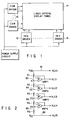
- a liquid crystal display panel 11 shown in FIG. 1 is basically designed such that a liquid crystal is sandwiched between two glass plates having a large number of wiring lines formed on their surfaces in orthogonal directions.
- a plurality of first electrodes (to be referred to as common electrodes hereinafter) (not shown) called common electrodes, scanning electrodes, or the like extend from the liquid crystal display panel 11 in the lateral direction
- a plurality of second electrodes (to be referred to as segment electrodes hereinafter) (not shown) called segment electrodes, data electrodes, or the like extend from the liquid crystal display panel 11 in the vertical direction.
- a segment consisting of a capacitor constituted by two wiring lines connected to the two electrodes and a liquid crystal located therebetween is turned on/driven. ON/OFF driving control of this segment is performed by using liquid crystal driving integrated circuits called a COM driver 12 on the common electrode side and a SEG driver 13 on the segment electrode side, respectively.
- the numbers of common electrodes and segment electrodes are considerably large, even though they vary depending on the type of a liquid crystal display panel.
- some liquid crystal display panel has 64 common electrodes and 160 segment electrodes.
- a plurality of COM drivers 12 and SEG drivers 13 are generally formed on the common side and the segment side, respectively.
- These COM drivers 12 and SEG drivers 13 generate driving signals on the basis of various types of control signals and display data, and supply the signals to the corresponding common and segment electrodes of the liquid crystal display panel 11.
- a plurality of liquid crystal driving voltages having different values are required. These voltages are generated by a power supply circuit 14.
- This power supply circuit 14 may be incorporated in any one of the COM drivers 12 or of the SEG drivers 13, or may be integrated into one integrated circuit together with all the COM and SEG drivers 12 and 13.
- a plurality of liquid crystal driving voltages having different values are formed by a voltage dividing operation using a plurality of resistors arranged between power supplies.
- the current driving abilities of the formed voltages are determined by the values of the voltage dividing resistors.
- the value of each voltage driving resistor may be increased. In this case, however, a large amount of current flows between the power supplies to increase the power consumption of the power supply circuit 14.
- the value of each voltage dividing resistor may be increased to decrease the amount of current flowing between the power supplies. In this case, however, the current driving ability at the node of each voltage deteriorates, and the voltage cannot be maintained if a large amount of current flows.
- FIG. 2 shows the arrangement of a power supply circuit using this power amplifier.
- voltages VDD and VEE are external power supply voltages which are externally applied.
- the value of the voltage VDD is set to 0V
- the value of the voltage VEE is set to -10V, which can be arbitrarily changed with -10V being set as the minimum value.
- Five voltage dividing resistors R1 to R5 are series-connected between a node 81 of the voltage VDD and a node 82 of the voltage VEE.
- resistors having high resistances are used to sufficiently decrease the value of a DC current flowing between the node 81 of the voltage VDD and the node 82 of the voltage VEE so as to restrict the power consumption to a small value.
- the resistors R1 and R2 located near the node of the voltage VDD, and the resistors R4 and R5 located near the node of the voltage VEE are all set to, for example, the same value.
- the resistor R3 between these resistors is set to, for example, a predetermined multiple of the value of the resistors R1, R2, R4, and R5.
- the voltage VDD, the voltage VEE, and four voltages obtained at series-connected nodes 83, 84, 85, and 86 of the respective resistors, i.e., a total of six voltages, are applied, as liquid crystal driving voltages VLC0, VLC1, VLC2, VLC3, VLC4, and VLC5, to the COM drivers 12 and the SEG drivers 13.
- liquid crystal driving voltages VLC0, VLC1, VLC2, VLC3, VLC4, and VLC5 are used as the common electrode driving voltages
- the voltages VLC0, VLC2, VLC3, and VLC5 are used as the segment driving voltages.
- voltages VLC0 and VLC5 which are identical to the external power supply voltages VDD and VEE, have sufficiently high current driving abilities
- voltages V1, V2, V3, and V4 which are formed by a voltage dividing operation using the resistors having high resistances, do not have sufficiently high current driving abilities.
- the divided voltages V1, V2, V3, and V4 are respectively received by power amplifiers AMP1, AMP2, AMP3, and AMP4, which are designed to perform impedance conversion, to obtain low-impedance outputs, which are applied, as the voltages VLC1, VLC2, VLC3, and VLC4, to the COM drivers 12 and the SEG drivers 13.
- amplifiers having CMOS structures constituted by p- and n-channel MOS transistors are used.
- Ntop type amplifiers constituted by n-channel MOS transistors for receiving input voltages are used.
- Ptop type amplifiers constituted by p-channel MOS transistor for receiving input voltages are used.
- each of the Ntop type power amplifiers AMP1 and AMP2 is constituted by a differential amplification stage 26 and an output stage 29.
- the differential amplification stage 26 includes p-channel MOS transistors 21 and 22 serving as a current mirror load, n-channel MOS transistors 23 and 24 serving as a differential input pair, and an n-channel MOS transistor 25 as a constant-current source.
- the output stage 29 includes a p-channel MOS transistor 27 as a driving transistor for receiving an output from the differential amplification stage 26, and an n-channel MOS transistor 28 as a constant-current source. Note that a bias voltage VNB is applied to the gate of each of the MOS transistors 25 and 28.
- each of the Ptop type power amplifiers AMP3 and AMP4 is constituted by a differential amplification stage 36 and an output stage 39.
- the differential amplification stage 36 includes n-channel MOS transistors 31 and 32 serving as a current mirror load, p-channel MOS transistors 33 and 34 serving as a differential input pair, and a p-channel MOS transistor 35 as a constant-current source.
- the output stage 39 includes an n-channel MOS transistor 37 as a driving transistor for receiving an output from the differential amplification stage 36, and a p-channel MOS transistor 38 as a constant-current source. Note that a bias voltage VPB is applied to the gate of each of the MOS transistors 35 and 38. Both capacitors C in FIGS. 3 and 4 serve to prevent oscillation so as to stabilize operations.
- FIG. 5 is a graph showing the voltage VEE dependencies of the respective liquid crystal driving voltages generated by the power supply circuit in FIG. 2, except for the voltage VLC0 identical to the voltage VDD, i.e., the voltage VEE dependencies of the voltages VLC1 to VLC5.
- the external power supply voltage VEE can be adjusted to freely set a display contrast to some extent.
- the contrast weakens
- the voltage changes toward -10V the contrast strengthens.
- the values of the voltages VLC0 to VLC5 become the maximum values (near 0V) when the voltage VEE is -6V, and become the minimum values (large negative values) when the voltage VEE is -10V.
- a power amplifier having an n-channel MOS transistor for receiving an input voltage i.e., an Ntop type power amplifier, does not operate unless the gate voltage (input voltage) of the n-channel MOS transistor 23 in FIG. 3 is higher than the source voltage by the corresponding threshold voltage or more.
- a power amplifier having a p-channel MOS transistor for receiving an input voltage i.e., a Ptop type power amplifier, does not operate unless the gate voltage (input voltage) of the p-channel MOS transistor 33 in FIG. 4 is lower than the source voltage by the absolute value of the corresponding threshold voltage or more. It is generally known that there are variations in the threshold voltage of a MOS transistor. Assume that the maximum absolute values of the threshold voltages of n- and p-channel MOS transistors are 1V, in consideration of such variations in threshold voltage. In this case, as shown in FIG.
- the input voltage range in which the Ntop type power amplifiers AMP1 and AMP2 (Ntop-Amps) satisfactorily operate is -8V or more when the voltage VEE is -10V.
- the input voltage range in which the Ptop type power amplifiers AMP3 and AMP4 (Ptop-Amps) satisfactorily operate is -2V or less when the voltage VEE is -10V.
- Ntop-Amps are used as the power amplifiers AMP1 and AMP2 for receiving voltages whose values may become -2V or more, whereas Ptop-Amps are used as the power amplifiers AMP3 and AMP4 for receiving voltages whose values may become -8V or less.
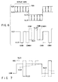
- FIG. 6 shows examples of the waveforms of a common driving signal COM and a segment driving signal SEG respectively output from the COM and SEG drivers 12 and 13 in FIG. 1.
- the segment driving signal SEG is formed by using the four liquid crystal driving voltages VLC0, VLC2, VLC3, and VLC5.
- the segment driving signal SEG is alternately switched in value between VLC0 and VLC2 every time display data changes in a given half period of a frame signal as a kind of control signal, and alternately switched in value between VLC3 and VLC5 every time the display data changes in the next half period of the frame signal.
- the common driving signal COM is formed by using the four liquid crystal driving voltages VLC0, VLC1, VLC4, and VLC5.
- common driving signals of 64 common driving signals COM1 to COM64, which have been set to VLC1 are sequentially switched to VLC5, starting from the common driving signal COM1.
- common driving signals which have been set to VLC4 are sequentially switched to VLC0, starting from the common driving signal COM1.
- one common driving signal COM is switched in value once for each half period of the frame signal, whereas the segment driving signal SEG is switched in value every time the display data changes.
- the frequency of the frame signal is 35 Hz
- the frequency of a latch pulse signal for the display data is 2,240 Hz. Therefore, the amount of current flowing from the node of each of the liquid crystal driving voltages VLC0, VLC2, VLC3, and VLC5 used to form the segment driving signal SEG is larger than the amount of current flowing from the node of each of the liquid crystal driving voltages VLC1 and VLC4 used only to form the common driving signal COM.
- FIG. 7 shows examples of the waveforms of the common driving signal COM and the segment driving signal SEG respectively applied to one common electrode and a corresponding segment electrode in the liquid crystal display panel in FIG. 1.
- the MOS transistor 27 for charging an output terminal 30 to the voltage VDD on the output stage 29 is driven by an output from the differential amplification stage 26, and the MOS transistor 28 for discharging the output terminal 30 to the voltage VEE serves as a constant-current source.
- the MOS transistor 28 as the constant-current source is restricted to a small value to reduce the power consumption of the power amplifier itself, the ability of increasing the output voltage to the voltage VDD is high, but the ability of decreasing the output voltage to the voltage VEE is low.
- the value of the voltage VLC2 of the segment driving signal SEG is increased toward the power supply voltage VDD (VLC0) and is sequentially increased toward the voltage VLC0.
- the MOS transistor 37 for discharging an output terminal 40 to the voltage VEE on the output stage 39 is driven by an output from the differential amplification stage 36, and the MOS transistor 38 for charging the output terminal 40 to the voltage VDD serves as a constant-current source.
- the MOS transistor 38 as the constant-current source is restricted to a small value to reduce the power consumption of the power amplifier itself, the ability of decreasing the output voltage to the voltage VEE is high, but the ability of increasing the output voltage to the voltage VDD is low. For this reason, as shown in FIG.
- the value of the voltage VLC3 of the segment driving signal SEG is decreased toward the power supply voltage VEE (VLC5) and is sequentially decreased toward the voltage VLC5.
- VEE power supply voltage
- FIG. 8 shows the detailed arrangement of the power supply circuit 14 in the electronic device in FIG. 1 according to the first embodiment of the present invention.
- the resistors R1, R2, R4, and R5 are all set to the same value.
- the resistor R3 between the resistors R2 and R4 is set to, for example, a predetermined multiple of the value of the resistors R1, R2, R4, and R5.
- the voltage VDD, the voltage VEE, and four voltages obtained at series-connected nodes 83, 84, 85, and 86 of the respective resistors, i.e., a total of six voltages, are applied, as liquid crystal driving voltages VLC0, VLC1, VLC2, VLC3, VLC4, and VLC5, to the COM drivers 12 and the SEG drivers 13 in the circuit shown in FIG. 1.
- the voltages VLC0, VLC1, VLC4, and VLC5 are used as the common electrode driving voltages, and the voltages VLC0, VLC2, VLC3, and VLC5 are used as the segment driving voltages.
- power amplifiers AMP11 to AMP14 used as impedance conversion means are respectively connected to the nodes 83, 84, 85, and 86 at which divided voltages V1, V2, V3, and V4 are obtained. Output voltages from these power amplifiers AMP11 to AMP14 are applied, as the liquid crystal driving voltages VLC1, VLC2, VLC3, and VLC4, to the COM and SEG drivers 12 and 13.
- the power amplifier AMP11 connected to the node 83 of the divided voltage V1 an Ntop type amplifier like the one described above is used.
- the power amplifier AMP12 connected to the node 84 of the divided voltage V2 a Ptop type amplifier like the one described above is used.
- FIG. 3 shows the detailed arrangement of the Ntop type power amplifiers AMP11 and AMP13. More specifically, each of the Ntop type power amplifiers AMP11 and AMP13 is constituted by a differential amplification stage 26 and an output stage 29.
- the differential amplification stage 26 includes p-channel MOS transistors 21 and 22 serving as a current mirror load, n-channel MOS transistors 23 and 24 serving as a differential input pair, and an n-channel MOS transistor 25 as a constant-current source.
- the output stage 29 includes a p-channel MOS transistor 27 as a driving transistor for receiving an output from the differential amplification stage 26, and an n-channel MOS transistor 28 as a constant-current source.
- FIG. 1 shows the detailed arrangement of the Ntop type power amplifiers AMP11 and AMP13. More specifically, each of the Ntop type power amplifiers AMP11 and AMP13 is constituted by a differential amplification stage 26 and an output stage 29.
- the differential amplification stage 26 includes p-channel
- each of the Ptop type power amplifiers AMP3 and AMP4 is constituted by a differential amplification stage 36 and an output stage 39.
- the differential amplification stage 36 includes n-channel MOS transistors 31 and 32 serving as a current mirror load, p-channel MOS transistors 33 and 34 serving as a differential input pair, and a p-channel MOS transistor 35 as a constant-current source.
- the output stage 39 includes an n-channel MOS transistor 37 as a driving transistor for receiving an output from the differential amplification stage 36, and a p-channel MOS transistor 38 as a constant-current source.
- the Ptop type power amplifier having the output stage 39 constituted by the n-channel MOS transistor 37 as a driving transistor and the p-channel MOS transistor 38 as a constant-current source is used as the power amplifier AMP12 for outputting the voltage VLC2, which poses a problem from the point of view that the amount of current flowing out of the amplifier is large and the value of the voltage VLC2 increases toward the voltage VLC2 when the liquid crystal display panel 11 shown in FIG. 1 performs a display operation.
- a sufficient amount of current can be caused to flow into the output terminal 40 by the n-channel MOS transistor 37.
- the Ntop type power amplifier having the output stage 29 constituted by the n-channel MOS transistor 27 as a driving transistor and the n-channel MOS transistor 28 as a constant-current source is used as the power amplifier AMP13 for outputting the voltage VLC3, which poses a problem from the point of view that the amount of current flowing out of the amplifier is large and the value of the voltage VLC3 decreases toward the voltage VLC5 when the liquid crystal display panel 11 performs a display operation.
- a sufficient amount of current can be caused to flow from the output terminal 30 by the p-channel MOS transistor 27.
- the external power supply voltage VEE is set to, e.g., -10V and can be arbitrarily changed.
- this power supply voltage a power supply voltage whose value can be arbitrarily changed up to -25 V can be used.
- FIG. 9 shows the circuit arrangement of a power supply circuit according to the second embodiment of the present invention.
- the value of the external power supply voltage VEE is changed to set a display contrast.
- a variable resistor RV is inserted between the resistor R5 in FIG. 8 and a node 82 of an external power supply voltage VEE having a fixed value, and the values of liquid crystal driving voltages VLC1 to VLC5 are changed by adjusting the variable resistor RV.
- a voltage V5 corresponding to the voltage VLC5 is also formed by a voltage dividing operation using resistors.
- a power amplifier AMP15 as an impedance conversion means is connected to a node 87 at which the voltage V5 is obtained.
- a Ptop type amplifier like the one shown in FIG. 4 may be used as this power amplifier AMP15.
- a Ptop type amplifier is used as a power amplifier AMP12 connected to a node 84 of a divided voltage V2
- an Ntop type amplifier is used as a power amplifier AMP13 connected to a node 85 of a divided voltage V3. That is, each of these circuits is of a reverse type to the circuit shown in FIG. 2.
- a Ptop type amplifier cannot be used in the circuit shown in FIG. 2 since the input voltage V2 to the power amplifier AMP2 becomes -2V or more, a Ptop type amplifier cannot be used. Hence, an Ntop type amplifier is used.
- the input voltage V3 to the power amplifier AMP3 becomes -8V or less, an Ntop type amplifier cannot be used.
- a Ptop type amplifier is used.
- this does not mean that the circuit does not operate at all if a Ptop type amplifier is used as the power amplifier AMP12 for receiving the voltage V2; and an Ntop type amplifier, as the power amplifier AMP13 for receiving the voltage V3.
- No problem is posed if the voltages V2 and V3 are carefully set, and the threshold voltages of the MOS transistors are set to be lower, while the values can be controlled with high precision. Therefore, in the embodiments shown in FIGS. 8 and 9, Ptop and Ntop type amplifiers may be used as the power amplifiers AMP12 and AMP13, respectively. It is, however, inevitable that the margins of the operating points of the power amplifiers AMP12 and AMP13 are reduced in the circuits of the embodiments shown in FIGS. 8 and 9.
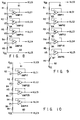
- FIG. 10 shows the arrangement of a power supply circuit according to the third embodiment of the present invention.
- the circuit of this embodiment shown in FIG. 10 is designed to realize low power consumption and stabilization of each liquid crystal driving voltage without reducing the margins of the operating points of power amplifiers connected to nodes 84 and 85 of voltages V2 and V3.
- an Ntop type power amplifier AMP22 is used in place of the Ptop type power amplifier AMP12 connected to the node 84 of the voltage V2
- a Ptop type power amplifier AMP23 is used in place of the Ntop type power amplifier AMP13 connected to the node 85 of the voltage V3.
- FIG. 11 shows the detailed arrangement of the Ntop type power amplifier AMP22 used in the circuit of the third embodiment.
- the Ntop type power amplifier AMP22 is constituted by a differential amplification stage 46, an intermediate output stage 49, and a final output stage 52.
- the differential amplification stage 46 includes p-channel MOS transistors 41 and 42 serving as a current mirror load, n-channel MOS transistors 43 and 44 serving as a differential input pair, and an n-channel MOS transistor 45 as a constant-current source.
- the intermediate output stage 49 includes a p-channel MOS transistor 47 as a driving transistor for receiving an output from the differential amplification stage 46, and an n-channel MOS transistor 48 as a constant-current source.
- the final output stage 52 includes an n-channel MOS transistor 50 as a driving transistor for receiving an output from the intermediate output stage 49, and a p-channel MOS transistor 51 as a constant-current source. Note that a predetermined bias voltage VNB is applied to the gate of each of the MOS transistors 45 and 48, and a predetermined bias voltage VPB is applied to the gate of the MOS transistor 51.
- an n-channel MOS transistor is used as the MOS transistor 43 for receiving the input voltage V2 on the differential amplification stage 46.
- a reduction in the margin of the operating point can be prevented, unlike the case wherein a p-channel MOS transistor is used.
- a sufficient amount of current can be caused to flow into the amplifier via an output terminal 53 by the n-channel MOS transistor 50. Therefore, a rise in the output voltage VLC2 toward the voltage VLC0 can be prevented, and the value of the voltage VLC2 can be stably maintained.
- FIG. 12 shows the detailed arrangement of the Ptop type power amplifier AMP23 used in the circuit of the third embodiment.
- the Ptop type power amplifier AMP23 is constituted by a differential amplification stage 66, an intermediate output stage 69, and a final output stage 72.
- the differential amplification stage 66 includes n-channel MOS transistors 61 and 62 serving as a current mirror load, p-channel MOS transistors 63 and 64 serving as a differential input pair, and a p-channel MOS transistor 65 as a constant-current source.
- the intermediate output stage 69 includes an n-channel MOS transistor 67 as a driving transistor for receiving an output from the differential amplification stage 66, and a p-channel MOS transistor 68 as a constant-current source.
- the final output stage 72 includes a p-channel MOS transistor 70 as a driving transistor for receiving an output from the intermediate output stage 69, and an n-channel MOS transistor 71 as a constant-current source. Note that the predetermined bias voltage VPM is applied to the gate of each of the MOS transistors 65 and 68, and the predetermined bias voltage VN is applied to the gate of the MOS transistor 71.
- a p-channel MOS transistor is used as the MOS transistor 63 for receiving the input voltage V3 on the differential amplification stage 64.
- a reduction in the margin of the operating point can be prevented, unlike the case wherein an n-channel MOS transistor is used.
- a sufficient amount of current can be caused to flow out of the amplifier via an output terminal 73 by the p-channel MOS transistor 70. Therefore, a drop in the output voltage VLC3 toward the voltage VLC5 can be prevented, and the value of the voltage VLC3 can be stably maintained.
- a liquid crystal driving power supply circuit capable of further reducing the current consumption can be provided.
Landscapes
- Engineering & Computer Science (AREA)
- Chemical & Material Sciences (AREA)
- Crystallography & Structural Chemistry (AREA)
- Physics & Mathematics (AREA)
- Computer Hardware Design (AREA)
- General Physics & Mathematics (AREA)
- Theoretical Computer Science (AREA)
- Liquid Crystal Display Device Control (AREA)
- Liquid Crystal (AREA)
- Amplifiers (AREA)
- Control Of Indicators Other Than Cathode Ray Tubes (AREA)
Abstract
Description
- The present invention relates to a liquid crystal driving power supply circuit for generating a plurality of power supply voltages having different values used to drive a liquid crystal display panel.
- Liquid crystal display panels have low power consumption and a small size. Owing to these advantages, the liquid crystal display panels are used as the display units of portable electronic devices such as electronic desk calculators and electronic pocketbooks. In order to drive such a liquid crystal display panel, a plurality of voltages having different values are required. These liquid crystal driving voltages are generally formed by a voltage dividing operation using a plurality of resistors arranged between power supplies. The maximum value of a current which can be caused to flow from the node of each voltage formed by such a voltage dividing operation is determined by the value of each of the plurality of resistors. Therefore, the amount of current flowing from the node of each voltage may be increased by decreasing the value of each resistor. In this case, however, a large amount of current flows between the power supplies, resulting in an increase in power consumption. On the other hand, in order to decrease this power consumption, the value of each resistance may be increased to decrease the amount of current flowing between the power supplies. In this case, however, the amount of current which can be caused to flow from the node of each voltage decreases. If a large current flows from each node, the voltage of each node decreases, and the value of each voltage cannot be maintained at a specified value.
- In general, in order to solve the above problem, a resistor having a high resistance is used as each voltage dividing resistor to achieve a reduction in power consumption, and each divided voltage is received by a power amplifier to achieve a reduction in the impedance of an output. The power amplifier has a differential input stage and an output stage. The differential input stage receives the respective divided voltages described above and an output voltage from the output stage connected to the differential input stage. The output stage has a constant-current source and a driving transistor to which an output from the differential input stage is supplied. Sufficiently large currents need to be supplied to the constant-current source and the driving transistor on the output stage to maintain an output voltage at a predetermined value even if a large current flows from or into the power amplifier. Consequently, the power consumption of the power amplifier increases, and the effect obtained by using a resistor having a high resistance as each voltage dividing resistor is reduced. This results in shortening the service life of a battery in a portable electronic device which is driven by the battery.
- It is, therefore, an object of the present invention to provide a liquid crystal driving power supply circuit which can further reduce the current consumption.
- According to the present invention, there is provided a liquid crystal driving power supply circuit comprising a first node to which a first power supply voltage is applied, a second node to which a second power supply voltage is applied, voltage dividing means for dividing a voltage between the first and second nodes into a plurality of voltages, first impedance conversion means, having a first output terminal and an ability of causing a current to flow from the first output terminal to the second node, the ability being set to be higher than an ability of causing a current to flow from the first node to the first output terminal, for receiving a first divided voltage obtained by the voltage dividing means and outputting a voltage corresponding to the first divided voltage, and second impedance conversion means, having a second output terminal and an ability of causing a current to flow from the first node to the second output terminal, the ability being set to be higher than an ability of causing a current to flow from the second output terminal to the second node, for receiving a second divided voltage having a value nearer to the second power supply voltage than the first divided voltage and obtained by the voltage dividing means, and for outputting a voltage corresponding to the second divided voltage.
- This invention can be more fully understood from the following detailed description when taken in conjunction with the accompanying drawings, in which:
- FIG. 1 is a block diagram showing a circuit arrangement around a display panel;
- FIG. 2 is a circuit diagram of a power supply circuit arranged in the circuit in FIG. 1;
- FIG. 3 is a circuit diagram of a power amplifier used in the power supply circuit in FIG. 2;
- FIG. 4 is a circuit diagram of another power amplifier used in the power supply circuit in FIG. 2;
- FIG. 5 is a graph showing the power supply voltage dependency of each liquid crystal driving voltage obtained by the power supply circuit in FIG. 2;
- FIG. 6 is a chart showing examples of the waveforms of a common driving signal and a segment driving signal, both generated by the circuit in FIG. 1;
- FIG. 7 is a chart showing examples of the waveforms of a common driving signal and a segment driving signal which are respectively supplied to one of the common electrodes in FIG. 6 and a segment electrode;
- FIG. 8 is a circuit diagram of the first embodiment of the present invention;
- FIG. 9 is a circuit diagram of the second embodiment of the present invention;
- FIG. 10 is a circuit diagram of the third embodiment of the present invention;
- FIG. 11 is a circuit diagram of a power amplifier used in the circuit of the third embodiment in FIG. 10;
- FIG. 12 is a circuit diagram of another power amplifier used in the circuit of the third embodiment in FIG. 10; and
- FIG. 13 is a circuit diagram of the fourth embodiment of the present invention.
- The above and other objects, features, and advantages of the present invention will be apparent from the following detailed description in conjunction with the accompanying drawings.
- A liquid crystal display panel 11 shown in FIG. 1 is basically designed such that a liquid crystal is sandwiched between two glass plates having a large number of wiring lines formed on their surfaces in orthogonal directions. In general, a plurality of first electrodes (to be referred to as common electrodes hereinafter) (not shown) called common electrodes, scanning electrodes, or the like extend from the liquid crystal display panel 11 in the lateral direction, whereas a plurality of second electrodes (to be referred to as segment electrodes hereinafter) (not shown) called segment electrodes, data electrodes, or the like extend from the liquid crystal display panel 11 in the vertical direction. When a predetermined potential is applied between one common electrode and a corresponding segment electrode, a segment consisting of a capacitor constituted by two wiring lines connected to the two electrodes and a liquid crystal located therebetween is turned on/driven. ON/OFF driving control of this segment is performed by using liquid crystal driving integrated circuits called a
COM driver 12 on the common electrode side and aSEG driver 13 on the segment electrode side, respectively. - In general, the numbers of common electrodes and segment electrodes are considerably large, even though they vary depending on the type of a liquid crystal display panel. For example, some liquid crystal display panel has 64 common electrodes and 160 segment electrodes. For this reason, a plurality of
COM drivers 12 andSEG drivers 13 are generally formed on the common side and the segment side, respectively. TheseCOM drivers 12 andSEG drivers 13 generate driving signals on the basis of various types of control signals and display data, and supply the signals to the corresponding common and segment electrodes of the liquid crystal display panel 11. In order to generate driving signals in theCOM drivers 12 and theSEG drivers 13, a plurality of liquid crystal driving voltages having different values are required. These voltages are generated by apower supply circuit 14. Thispower supply circuit 14 may be incorporated in any one of theCOM drivers 12 or of theSEG drivers 13, or may be integrated into one integrated circuit together with all the COM andSEG drivers - In general, a plurality of liquid crystal driving voltages having different values are formed by a voltage dividing operation using a plurality of resistors arranged between power supplies. The current driving abilities of the formed voltages are determined by the values of the voltage dividing resistors. In order to improve the current driving ability of each voltage, i.e., increase the amount of current flowing from the node of each voltage, the value of each voltage driving resistor may be increased. In this case, however, a large amount of current flows between the power supplies to increase the power consumption of the
power supply circuit 14. On the other hand, in order to reduce the power consumption, the value of each voltage dividing resistor may be increased to decrease the amount of current flowing between the power supplies. In this case, however, the current driving ability at the node of each voltage deteriorates, and the voltage cannot be maintained if a large amount of current flows. - In order to eliminate the above contradiction, each voltage obtained by a voltage dividing operation is generally received by a power amplifier. FIG. 2 shows the arrangement of a power supply circuit using this power amplifier. Referring to FIG. 2, voltages VDD and VEE are external power supply voltages which are externally applied. For example, the value of the voltage VDD is set to 0V, and the value of the voltage VEE is set to -10V, which can be arbitrarily changed with -10V being set as the minimum value. Five voltage dividing resistors R1 to R5 are series-connected between a
node 81 of the voltage VDD and anode 82 of the voltage VEE. As these voltage dividing resistors R1 to R5, resistors having high resistances are used to sufficiently decrease the value of a DC current flowing between thenode 81 of the voltage VDD and thenode 82 of the voltage VEE so as to restrict the power consumption to a small value. In general, of the five resistors, the resistors R1 and R2 located near the node of the voltage VDD, and the resistors R4 and R5 located near the node of the voltage VEE are all set to, for example, the same value. The resistor R3 between these resistors is set to, for example, a predetermined multiple of the value of the resistors R1, R2, R4, and R5. The voltage VDD, the voltage VEE, and four voltages obtained at series-connectednodes COM drivers 12 and theSEG drivers 13. For example, in theCOM drivers 12 and theSEG drivers 13, the voltages VLC0, VLC1, VLC4, and VLC5 are used as the common electrode driving voltages, and the voltages VLC0, VLC2, VLC3, and VLC5 are used as the segment driving voltages. - Although the voltages VLC0 and VLC5, which are identical to the external power supply voltages VDD and VEE, have sufficiently high current driving abilities, voltages V1, V2, V3, and V4, which are formed by a voltage dividing operation using the resistors having high resistances, do not have sufficiently high current driving abilities. For this reason, as shown in FIG. 2, the divided voltages V1, V2, V3, and V4 are respectively received by power amplifiers AMP1, AMP2, AMP3, and AMP4, which are designed to perform impedance conversion, to obtain low-impedance outputs, which are applied, as the voltages VLC1, VLC2, VLC3, and VLC4, to the
COM drivers 12 and theSEG drivers 13. - As the above power amplifiers, amplifiers having CMOS structures constituted by p- and n-channel MOS transistors are used. As the two power amplifiers AMP1 and AMP2 for receiving the divided voltages V1 and V2 near the voltage VDD, Ntop type amplifiers constituted by n-channel MOS transistors for receiving input voltages are used. As the two power amplifiers AMP3 and AMP4 near the voltage VEE, Ptop type amplifiers constituted by p-channel MOS transistor for receiving input voltages are used.
- As shown in FIG. 3, each of the Ntop type power amplifiers AMP1 and AMP2 is constituted by a
differential amplification stage 26 and anoutput stage 29. Thedifferential amplification stage 26 includes p-channel MOS transistors channel MOS transistors channel MOS transistor 25 as a constant-current source. Theoutput stage 29 includes a p-channel MOS transistor 27 as a driving transistor for receiving an output from thedifferential amplification stage 26, and an n-channel MOS transistor 28 as a constant-current source. Note that a bias voltage VNB is applied to the gate of each of theMOS transistors - As shown in FIG. 4, each of the Ptop type power amplifiers AMP3 and AMP4 is constituted by a
differential amplification stage 36 and anoutput stage 39. Thedifferential amplification stage 36 includes n-channel MOS transistors channel MOS transistors channel MOS transistor 35 as a constant-current source. Theoutput stage 39 includes an n-channel MOS transistor 37 as a driving transistor for receiving an output from thedifferential amplification stage 36, and a p-channel MOS transistor 38 as a constant-current source. Note that a bias voltage VPB is applied to the gate of each of theMOS transistors - FIG. 5 is a graph showing the voltage VEE dependencies of the respective liquid crystal driving voltages generated by the power supply circuit in FIG. 2, except for the voltage VLC0 identical to the voltage VDD, i.e., the voltage VEE dependencies of the voltages VLC1 to VLC5. In a general liquid crystal display panel, the external power supply voltage VEE can be adjusted to freely set a display contrast to some extent. In general, as the voltage VEE is changed toward -6V, the contrast weakens, whereas as the voltage changes toward -10V, the contrast strengthens. The values of the voltages VLC0 to VLC5 become the maximum values (near 0V) when the voltage VEE is -6V, and become the minimum values (large negative values) when the voltage VEE is -10V.
- Voltages exhibiting changes like those shown in FIG. 5 are input to the four power amplifiers AMP1 to AMP4. For this reason, as the power amplifiers AMP1 to AMP4, amplifiers having performance levels corresponding to the respective input voltages must be selected. A power amplifier having an n-channel MOS transistor for receiving an input voltage, i.e., an Ntop type power amplifier, does not operate unless the gate voltage (input voltage) of the n-
channel MOS transistor 23 in FIG. 3 is higher than the source voltage by the corresponding threshold voltage or more. A power amplifier having a p-channel MOS transistor for receiving an input voltage, i.e., a Ptop type power amplifier, does not operate unless the gate voltage (input voltage) of the p-channel MOS transistor 33 in FIG. 4 is lower than the source voltage by the absolute value of the corresponding threshold voltage or more. It is generally known that there are variations in the threshold voltage of a MOS transistor. Assume that the maximum absolute values of the threshold voltages of n- and p-channel MOS transistors are 1V, in consideration of such variations in threshold voltage. In this case, as shown in FIG. 5, the input voltage range in which the Ntop type power amplifiers AMP1 and AMP2 (Ntop-Amps) satisfactorily operate is -8V or more when the voltage VEE is -10V. The input voltage range in which the Ptop type power amplifiers AMP3 and AMP4 (Ptop-Amps) satisfactorily operate is -2V or less when the voltage VEE is -10V. - In this case, Ntop-Amps are used as the power amplifiers AMP1 and AMP2 for receiving voltages whose values may become -2V or more, whereas Ptop-Amps are used as the power amplifiers AMP3 and AMP4 for receiving voltages whose values may become -8V or less.
- FIG. 6 shows examples of the waveforms of a common driving signal COM and a segment driving signal SEG respectively output from the COM and
SEG drivers - As is apparent from FIG. 6, one common driving signal COM is switched in value once for each half period of the frame signal, whereas the segment driving signal SEG is switched in value every time the display data changes. For example, the frequency of the frame signal is 35 Hz, and the frequency of a latch pulse signal for the display data is 2,240 Hz. Therefore, the amount of current flowing from the node of each of the liquid crystal driving voltages VLC0, VLC2, VLC3, and VLC5 used to form the segment driving signal SEG is larger than the amount of current flowing from the node of each of the liquid crystal driving voltages VLC1 and VLC4 used only to form the common driving signal COM.
- FIG. 7 shows examples of the waveforms of the common driving signal COM and the segment driving signal SEG respectively applied to one common electrode and a corresponding segment electrode in the liquid crystal display panel in FIG. 1. When the amount of current flowing from the node of each of the liquid crystal driving voltages VLC0, VLC2, VLC3, and VLC5 used to form the segment driving signal SEG is large, as described above, no problem is posed with respect to the voltages VLC0 and VLC5 identical to the external power supply voltages VDD and VEE, but a problem is posed with respect to the voltages VLC2 and VLC3 output from the power amplifiers AMP2 and AMP3 in FIG. 2. More specifically, in the Ntop type power amplifier AMP2 for outputting the voltage VLC2, as shown in FIG. 3, the
MOS transistor 27 for charging anoutput terminal 30 to the voltage VDD on theoutput stage 29 is driven by an output from thedifferential amplification stage 26, and theMOS transistor 28 for discharging theoutput terminal 30 to the voltage VEE serves as a constant-current source. For this reason, if a current flowing in theMOS transistor 28 as the constant-current source is restricted to a small value to reduce the power consumption of the power amplifier itself, the ability of increasing the output voltage to the voltage VDD is high, but the ability of decreasing the output voltage to the voltage VEE is low. For this reason, as shown in FIG. 7, the value of the voltage VLC2 of the segment driving signal SEG is increased toward the power supply voltage VDD (VLC0) and is sequentially increased toward the voltage VLC0. In contrast to this, in the Ptop type power amplifier AMP3 for outputting the voltage VLC3, as shown in FIG. 4, theMOS transistor 37 for discharging anoutput terminal 40 to the voltage VEE on theoutput stage 39 is driven by an output from thedifferential amplification stage 36, and theMOS transistor 38 for charging theoutput terminal 40 to the voltage VDD serves as a constant-current source. For this reason, if a current flowing in theMOS transistor 38 as the constant-current source is restricted to a small value to reduce the power consumption of the power amplifier itself, the ability of decreasing the output voltage to the voltage VEE is high, but the ability of increasing the output voltage to the voltage VDD is low. For this reason, as shown in FIG. 7, the value of the voltage VLC3 of the segment driving signal SEG is decreased toward the power supply voltage VEE (VLC5) and is sequentially decreased toward the voltage VLC5. In order to prevent such variations in output voltage, a relatively large current is supplied to the constant-current source of each power amplifier to simultaneously improve both the abilities of causing a current to flow into and out of each power amplifier through the output terminal. With this operation, the output impedances of all the power amplifiers are decreased to prevent the above-described variations in output voltage. - If, however, large currents flow in the constant-current source of all the power amplifiers, the current consumption of each power amplifier increases, resulting in a reduction in the effect of reducing the power consumption which is obtained by using resistors having high resistances as voltage dividing resistors. Especially in a portable electronic device driven by a battery, the service life of the battery is shortened.
- FIG. 8 shows the detailed arrangement of the
power supply circuit 14 in the electronic device in FIG. 1 according to the first embodiment of the present invention. - Voltages VDD and VEE are external power supply voltages which are externally applied. For example, the value of the external power supply voltage VDD is set to 0V, and the value of the external power supply voltage VEE is set to -10V, which can be arbitrarily changed with -10V being set as the minimum value. Five voltage dividing resistors R1 to R5 are series-connected between a
node 81 of the voltage VDD and anode 82 of the voltage VEE. As these voltage dividing resistors R1 to R5, resistors having high resistances are used to sufficiently decrease the value of a DC current flowing between thenode 81 of the voltage VDD and thenode 82 of the voltage VEE so as to restrict the power consumption to a small value. Similar to the circuit shown in FIG. 2, for example, the resistors R1, R2, R4, and R5 are all set to the same value. The resistor R3 between the resistors R2 and R4 is set to, for example, a predetermined multiple of the value of the resistors R1, R2, R4, and R5. The voltage VDD, the voltage VEE, and four voltages obtained at series-connectednodes COM drivers 12 and theSEG drivers 13 in the circuit shown in FIG. 1. In theCOM drivers 12 and theSEG drivers 13, the voltages VLC0, VLC1, VLC4, and VLC5 are used as the common electrode driving voltages, and the voltages VLC0, VLC2, VLC3, and VLC5 are used as the segment driving voltages. - In the circuit of this embodiment, power amplifiers AMP11 to AMP14 used as impedance conversion means are respectively connected to the
nodes SEG drivers node 83 of the divided voltage V1, an Ntop type amplifier like the one described above is used. As the power amplifier AMP12 connected to thenode 84 of the divided voltage V2, a Ptop type amplifier like the one described above is used. As the power amplifier AMP13 connected to thenode 85 of the divided voltage V3, an Ntop type amplifier like the one described above is used. As the power amplifier AMP14 connected to thenode 86 of the divided voltage V4, a Ptop type amplifier like the one described above is used. - FIG. 3 shows the detailed arrangement of the Ntop type power amplifiers AMP11 and AMP13. More specifically, each of the Ntop type power amplifiers AMP11 and AMP13 is constituted by a
differential amplification stage 26 and anoutput stage 29. Thedifferential amplification stage 26 includes p-channel MOS transistors channel MOS transistors channel MOS transistor 25 as a constant-current source. Theoutput stage 29 includes a p-channel MOS transistor 27 as a driving transistor for receiving an output from thedifferential amplification stage 26, and an n-channel MOS transistor 28 as a constant-current source. FIG. 4 shows the detailed arrangement of the Ptop type power amplifiers AMP12 and AMP14. More specifically, each of the Ptop type power amplifiers AMP3 and AMP4 is constituted by adifferential amplification stage 36 and anoutput stage 39. Thedifferential amplification stage 36 includes n-channel MOS transistors channel MOS transistors channel MOS transistor 35 as a constant-current source. Theoutput stage 39 includes an n-channel MOS transistor 37 as a driving transistor for receiving an output from thedifferential amplification stage 36, and a p-channel MOS transistor 38 as a constant-current source. - Consider the liquid crystal driving voltages VLC2 and VLC3, which pose problems as described above.
- As shown in FIG. 4, the Ptop type power amplifier having the
output stage 39 constituted by the n-channel MOS transistor 37 as a driving transistor and the p-channel MOS transistor 38 as a constant-current source is used as the power amplifier AMP12 for outputting the voltage VLC2, which poses a problem from the point of view that the amount of current flowing out of the amplifier is large and the value of the voltage VLC2 increases toward the voltage VLC2 when the liquid crystal display panel 11 shown in FIG. 1 performs a display operation. In this Ptop type power amplifier, a sufficient amount of current can be caused to flow into theoutput terminal 40 by the n-channel MOS transistor 37. Therefore, a rise in the output voltage VLC2 toward the voltage VLC0 can be prevented, and the value of the voltage VLC2 can be stably maintained. For this reason, with regard to the p-channel MOS transistor 38 used as a constant-current source in theoutput stage 39, the value of the output voltage is only required to be maintained, but a large current need not be supplied. When the voltage VLC2 at theoutput terminal 40 is lower than a specified value, a current flows in theMOS transistor 38. Otherwise, a current flows in theMOS transistor 38 via theMOS transistor 37. For this reason, a current is always consumed by theMOS transistor 38. However, as described above, since a large current need not be supplied to the p-channel MOS transistor 38, this current value can be reduced. - As shown in FIG. 3, the Ntop type power amplifier having the
output stage 29 constituted by the n-channel MOS transistor 27 as a driving transistor and the n-channel MOS transistor 28 as a constant-current source is used as the power amplifier AMP13 for outputting the voltage VLC3, which poses a problem from the point of view that the amount of current flowing out of the amplifier is large and the value of the voltage VLC3 decreases toward the voltage VLC5 when the liquid crystal display panel 11 performs a display operation. In this Ntop type power amplifier, a sufficient amount of current can be caused to flow from theoutput terminal 30 by the p-channel MOS transistor 27. Therefore, a drop in the output voltage VLC2 toward the voltage VLC5 can be prevented, and the value of the voltage VLC3 can be stably maintained. For this reason, with regard to the p-channel MOS transistor 38 used as a constant-current source in theoutput stage 39, the value of the output voltage is only required to be maintained, but a large current need not be supplied. With regard to the n-channel MOS transistor 28 used as a constant-current source in theoutput stage 29, the value of the output voltage is only required to be maintained, and a large current need not be supplied. When the voltage VLC3 at theoutput terminal 30 is higher than a specified value, a current flows in theMOS transistor 28. Otherwise, a current flows in theMOS transistor 28 via theMOS transistor 27. For this reason, a current is always consumed by theMOS transistor 28. However, as described above, since a large current need not be supplied to the p-channel MOS transistor 28, this current value can be reduced. With regard to the remaining power amplifiers AMP11 and AMP14, variations in output voltage do not easily occur, and hence low current consumption can be realized. According to this embodiment, therefore, low power consumption can be realized in all the power amplifiers AMP11, AMP12, AMP13, and AMP14, and each liquid crystal driving voltage can be stabilized. - In the above embodiment, the external power supply voltage VEE is set to, e.g., -10V and can be arbitrarily changed. For example, as this power supply voltage, a power supply voltage whose value can be arbitrarily changed up to -25 V can be used.
- FIG. 9 shows the circuit arrangement of a power supply circuit according to the second embodiment of the present invention. In the circuit of the embodiment shown in FIG. 8, the value of the external power supply voltage VEE is changed to set a display contrast. In the second embodiment, a variable resistor RV is inserted between the resistor R5 in FIG. 8 and a
node 82 of an external power supply voltage VEE having a fixed value, and the values of liquid crystal driving voltages VLC1 to VLC5 are changed by adjusting the variable resistor RV. In this case, a voltage V5 corresponding to the voltage VLC5 is also formed by a voltage dividing operation using resistors. For this reason, a power amplifier AMP15 as an impedance conversion means is connected to anode 87 at which the voltage V5 is obtained. Note that a Ptop type amplifier like the one shown in FIG. 4 may be used as this power amplifier AMP15. - In the power supply circuits of the embodiments respectively shown in FIGS. 8 and 9, a Ptop type amplifier is used as a power amplifier AMP12 connected to a
node 84 of a divided voltage V2, and an Ntop type amplifier is used as a power amplifier AMP13 connected to anode 85 of a divided voltage V3. That is, each of these circuits is of a reverse type to the circuit shown in FIG. 2. As described with reference to FIG. 5, in the circuit shown in FIG. 2, since the input voltage V2 to the power amplifier AMP2 becomes -2V or more, a Ptop type amplifier cannot be used. Hence, an Ntop type amplifier is used. In addition, since the input voltage V3 to the power amplifier AMP3 becomes -8V or less, an Ntop type amplifier cannot be used. Hence, a Ptop type amplifier is used. However, this does not mean that the circuit does not operate at all if a Ptop type amplifier is used as the power amplifier AMP12 for receiving the voltage V2; and an Ntop type amplifier, as the power amplifier AMP13 for receiving the voltage V3. No problem is posed if the voltages V2 and V3 are carefully set, and the threshold voltages of the MOS transistors are set to be lower, while the values can be controlled with high precision. Therefore, in the embodiments shown in FIGS. 8 and 9, Ptop and Ntop type amplifiers may be used as the power amplifiers AMP12 and AMP13, respectively. It is, however, inevitable that the margins of the operating points of the power amplifiers AMP12 and AMP13 are reduced in the circuits of the embodiments shown in FIGS. 8 and 9. - FIG. 10 shows the arrangement of a power supply circuit according to the third embodiment of the present invention. The circuit of this embodiment shown in FIG. 10 is designed to realize low power consumption and stabilization of each liquid crystal driving voltage without reducing the margins of the operating points of power amplifiers connected to
nodes node 84 of the voltage V2, and a Ptop type power amplifier AMP23 is used in place of the Ntop type power amplifier AMP13 connected to thenode 85 of the voltage V3. Note that as power amplifiers AMP11 and AMP14 connected tonode - FIG. 11 shows the detailed arrangement of the Ntop type power amplifier AMP22 used in the circuit of the third embodiment. The Ntop type power amplifier AMP22 is constituted by a
differential amplification stage 46, anintermediate output stage 49, and afinal output stage 52. Thedifferential amplification stage 46 includes p-channel MOS transistors channel MOS transistors channel MOS transistor 45 as a constant-current source. Theintermediate output stage 49 includes a p-channel MOS transistor 47 as a driving transistor for receiving an output from thedifferential amplification stage 46, and an n-channel MOS transistor 48 as a constant-current source. Thefinal output stage 52 includes an n-channel MOS transistor 50 as a driving transistor for receiving an output from theintermediate output stage 49, and a p-channel MOS transistor 51 as a constant-current source. Note that a predetermined bias voltage VNB is applied to the gate of each of theMOS transistors MOS transistor 51. - In the power amplifier having the above arrangement, an n-channel MOS transistor is used as the
MOS transistor 43 for receiving the input voltage V2 on thedifferential amplification stage 46. With this arrangement, a reduction in the margin of the operating point can be prevented, unlike the case wherein a p-channel MOS transistor is used. In addition, on thefinal output stage 52, a sufficient amount of current can be caused to flow into the amplifier via anoutput terminal 53 by the n-channel MOS transistor 50. Therefore, a rise in the output voltage VLC2 toward the voltage VLC0 can be prevented, and the value of the voltage VLC2 can be stably maintained. - FIG. 12 shows the detailed arrangement of the Ptop type power amplifier AMP23 used in the circuit of the third embodiment. The Ptop type power amplifier AMP23 is constituted by a
differential amplification stage 66, anintermediate output stage 69, and afinal output stage 72. Thedifferential amplification stage 66 includes n-channel MOS transistors channel MOS transistors channel MOS transistor 65 as a constant-current source. Theintermediate output stage 69 includes an n-channel MOS transistor 67 as a driving transistor for receiving an output from thedifferential amplification stage 66, and a p-channel MOS transistor 68 as a constant-current source. Thefinal output stage 72 includes a p-channel MOS transistor 70 as a driving transistor for receiving an output from theintermediate output stage 69, and an n-channel MOS transistor 71 as a constant-current source. Note that the predetermined bias voltage VPM is applied to the gate of each of theMOS transistors MOS transistor 71. - In the power amplifier having the above arrangement, a p-channel MOS transistor is used as the
MOS transistor 63 for receiving the input voltage V3 on thedifferential amplification stage 64. With this arrangement, a reduction in the margin of the operating point can be prevented, unlike the case wherein an n-channel MOS transistor is used. In addition, in thefinal output stage 72, a sufficient amount of current can be caused to flow out of the amplifier via anoutput terminal 73 by the p-channel MOS transistor 70. Therefore, a drop in the output voltage VLC3 toward the voltage VLC5 can be prevented, and the value of the voltage VLC3 can be stably maintained. - FIG. 13 shows a power supply circuit according to the fourth embodiment of the present invention. In the circuit of the embodiment shown in FIG. 10, the external power supply voltage VEE is changed to set a display contrast. In the fourth embodiment, a variable resistor RV is inserted between the resistor R5 in FIG. 10 and an external power supply voltage VEE having a fixed value, and the values of liquid crystal driving voltages VLC1 to VLC5 are changed by adjusting the variable resistor RV. In this case, a voltage V5 corresponding to the voltage VLC5 is also formed by a voltage dividing operation using resistors. For this reason, a power amplifier AMP15 as an impedance conversion means is connected to a
node 87 of this voltage V5. Note that a Ptop type amplifier like the one shown in FIG. 4 can be used as this power amplifier AMP15. - As has been described above, according to the present invention, a liquid crystal driving power supply circuit capable of further reducing the current consumption can be provided.
Claims (11)
- A liquid crystal driving power supply circuit comprising:
a first node (81) to which a first power supply voltage (VDD) is applied;
a second node (82) to which a second power supply voltage (VEE) is applied;
voltage dividing means (R1 - R5) for dividing a voltage between said first and second nodes into a plurality of voltages;
first impedance conversion means (AMP12; AMP22), having a first output terminal (40) and an ability of causing a current to flow from the first output terminal to said second node, the ability being set to be higher than an ability of causing a current to flow from said first node to the first output terminal, for receiving a first divided voltage (V2) obtained by said voltage dividing means and outputting a voltage corresponding to the first divided voltage; and
second impedance conversion means (AMP13; AMP23), having a second output terminal (30) and an ability of causing a current to flow from said first node to the second output terminal, the ability being set to be higher than an ability of causing a current to flow from the second output terminal to said second node, for receiving a second divided voltage (V3) having a value nearer to the second power supply voltage than the first divided voltage and obtained by said voltage dividing means, and for outputting a voltage corresponding to the second divided voltage. - A circuit according to claim 1, characterized in that said voltage dividing means is constituted by a plurality of resistors (R1 - R5) connected in series between said first and second nodes.
- A circuit according to claim 1, characterized in that said first impedance conversion means (AMP12) includes
an n-channel MOS transistor (37), having a source, a drain, and a gate and a source-drain path connected between the first output terminal and said second node, for receiving a voltage corresponding to the first divided voltage at the gate, and
a first current source (38) connected between said first node and the first output terminal, and
said second impedance conversion means (AMP13) includes
a p-channel MOS transistor (27), having a source, drain, and gate and a source-drain path connected between said first node and the second output terminal, for receiving a voltage corresponding to the second divided voltage at the gate, and
a second current source (28) connected between the second output terminal and said second node. - A circuit according to claim 3, characterized in that the first current source is constituted by a p-channel MOS transistor having a gate to which a predetermined bias voltage is applied, and the second current source is constituted by an n-channel MOS transistor having a gate to which a predetermined bias voltage is applied.
- A circuit according to claim 1, characterized in that said first impedance conversion means (AMP12) is constituted by
a first differential amplification stage (36) including a p-channel first MOS transistor (33), having a source, a drain, and a gate, for receiving the first divided voltage at the gate, and
a first output stage (39) including an n-channel second MOS transistor (37), having a source, a drain, and a gate and a source-drain path connected between the first output terminal and said second node, for receiving an output voltage from said first differential amplification stage at the gate, and a first current source (38) connected between said first node and the first output terminal, and
said second impedance conversion means (AMP13) is constituted by
a second differential amplification stage (26) including an n-channel third MOS transistor (23), having a source, a drain, and a gate, for receiving the second divided voltage at the gate, and
a second output stage (29) including a p-channel fourth MOS transistor (27), having a source, a drain, and a gate and a source-drain path connected between said first node and the second output terminal, for receiving an output voltage from said second differential amplification stage at the gate, and a second current source (28) connected between the second output terminal and said second node. - A circuit according to claim 5, characterized in that the first current source is constituted by a p-channel MOS transistor having a gate to which a predetermined bias voltage is applied, and the second current source is constituted by an n-channel MOS transistor having a gate to which a predetermined bias voltage is applied.
- A circuit according to claim 1, characterized in that said first impedance conversion means (AMP12) is constituted by
a first differential amplification stage (36) including a p-channel first MOS transistor (33), having a source, a drain, and a gate, for receiving the first divided voltage at the gate, a p-channel second MOS transistor (34) having a source, a drain, and a gate and constituting a first differential pair together with the first MOS transistor, n-channel third and fourth MOS transistors (31, 32) constituting a current mirror load with respect to the first and second MOS transistors, and a first current source (35) for supplying a current to the first differential pair, and
a first output stage (39) including an n-channel fifth MOS transistor (37), having a source, drain, and a gate and a source-drain path connected between the first output terminal and said second node, for receiving an output voltage from the first differential amplification stage at the gate, and a second current source (38) connected between said first node and the first output terminal, and
said second impedance conversion means (AMP13) is constituted by
a second differential amplification stage (26) including an n-channel sixth MOS transistor (23), having a source, a drain, and a gate, for receiving the second divided voltage at the gate, an n-channel seventh MOS transistor (24) having a source, a drain, and a gate and constituting a second differential pair together with the sixth MOS transistor, p-channel eighth and ninth MOS transistors (21, 22) constituting a current mirror load with respect to the sixth and seventh MOS transistors, and a third current source (25) for supplying a current to the second differential pair, and
a second output stage (29) including an n-channel tenth MOS transistor (27), having a source, drain, and a gate and a source-drain path connected between the second output terminal and said second node, for receiving an output voltage from the second differential amplification stage at the gate, and a fourth current source (28) connected between said first node and the second output terminal. - A circuit according to claim 7, characterized in that each of the first and second current sources is constituted by a p-channel MOS transistor having a gate to which a predetermined bias voltage is applied, and each of the third and fourth current sources is constituted by an n-channel MOS transistor having a gate to which a predetermined bias voltage is applied.
- A circuit according to claim 1, characterized by further comprising:
third impedance conversion means (AMP11), having a third output terminal, for receiving a third divided voltage (V1) having a value nearer to the first power supply voltage than the first divided voltage and obtained by said voltage dividing means, and for outputting a voltage corresponding to the third divided voltage from the third output terminal; and
fourth impedance conversion means (AMP14), having a fourth output terminal, for receiving a fourth divided voltage (V4) having a value nearer to the second power supply voltage than the second divided voltage and obtained by said voltage dividing means, and for outputting a voltage corresponding to the fourth divided voltage from the fourth output terminal. - A circuit according to claim 9, characterized in that said third impedance conversion means (AMP11) is constituted by
a first differential amplification stage (26) including an n-channel first MOS transistor (23), having a source, a drain, and a gate, for receiving the third divided voltage at the gate, an n-channel second MOS transistor (24) having a source, a drain, and a gate and constituting a first differential pair together with the first MOS transistor, p-channel third and fourth MOS transistors (21, 22) constituting a current mirror load with respect to the first and second MOS transistors, and a first current source (25) for supplying a current to the first differential pair, and
a first output stage (29) including a p-channel fifth MOS transistor (27), having a source, drain, and a gate and a source-drain path connected between the second output terminal and said second node, for receiving an output voltage from the first differential amplification stage at the gate, and a fourth current source (28) connected between said first node and the third output terminal, and
said fourth impedance conversion means (AMP14) is constituted by
a second differential amplification stage (36) including a p-channel sixth MOS transistor (33), having a source, a drain, and a gate, for receiving the fourth divided voltage at the gate, a p-channel seventh MOS transistor (34) having a source, a drain, and a gate and constituting a second differential pair together with the sixth MOS transistor, n-channel eighth and ninth MOS transistors (31, 32) constituting a current mirror load with respect to the sixth and seventh MOS transistors, and a second current source (35) for supplying a current to the second differential pair. - A liquid crystal driving power supply circuit comprising:
voltage generating means (R1 - R5) for generating a plurality of potentials from the voltage externally applied; and
a plurality of impedance conversion means (AMP12, AMP13; AMP22, AMP23) connected to said potentials, respectively, each impedance conversion means having a diving device for driving an output,
wherein the driving device of each impedance conversion means is of N type in order to change the output toward a low potential and is of P type in order to change the output toward a high potential.
Applications Claiming Priority (2)
| Application Number | Priority Date | Filing Date | Title |
|---|---|---|---|
| JP10842193A JP3234043B2 (en) | 1993-05-10 | 1993-05-10 | Power supply circuit for driving LCD |
| JP108421/93 | 1993-05-10 |
Publications (3)
| Publication Number | Publication Date |
|---|---|
| EP0631269A2 true EP0631269A2 (en) | 1994-12-28 |
| EP0631269A3 EP0631269A3 (en) | 1995-02-15 |
| EP0631269B1 EP0631269B1 (en) | 1999-04-21 |
Family
ID=14484344
Family Applications (1)
| Application Number | Title | Priority Date | Filing Date |
|---|---|---|---|
| EP94107248A Expired - Lifetime EP0631269B1 (en) | 1993-05-10 | 1994-05-09 | Liquid crystal driving power supply circuit |
Country Status (6)
| Country | Link |
|---|---|
| US (1) | US6028598A (en) |
| EP (1) | EP0631269B1 (en) |
| JP (1) | JP3234043B2 (en) |
| KR (1) | KR0147249B1 (en) |
| CN (1) | CN1064470C (en) |
| DE (1) | DE69417956T2 (en) |
Cited By (4)
| Publication number | Priority date | Publication date | Assignee | Title |
|---|---|---|---|---|
| US5627457A (en) * | 1993-07-21 | 1997-05-06 | Seiko Epson Corporation | Power supply device, liquid crystal display device, and method of supplying power |
| GB2311631A (en) * | 1993-07-21 | 1997-10-01 | Seiko Epson Corp | Controlling power supply for liquid crystal display |
| EP0957466A1 (en) * | 1997-02-27 | 1999-11-17 | Citizen Watch Co., Ltd. | Circuit and method for driving liquid crystal display device |
| EP1081675A2 (en) * | 1999-08-30 | 2001-03-07 | Rohm Co., Ltd. | A power circuit for a liquid crystal display |
Families Citing this family (23)
| Publication number | Priority date | Publication date | Assignee | Title |
|---|---|---|---|---|
| JP3488054B2 (en) * | 1997-09-12 | 2004-01-19 | Necエレクトロニクス株式会社 | LCD drive device |
| JPH11242204A (en) * | 1998-02-25 | 1999-09-07 | Sony Corp | Liquid crystal display device and driving circuit therefor |
| JPH11252903A (en) * | 1998-03-03 | 1999-09-17 | Seiko Instruments Inc | Power circuit |
| JP3132470B2 (en) | 1998-06-08 | 2001-02-05 | 日本電気株式会社 | Power supply circuit for driving liquid crystal display panel and method of reducing power consumption |
| US6342782B1 (en) | 1999-01-08 | 2002-01-29 | Seiko Epson Corporation | Power supply device for driving liquid crystal, liquid crystal device and electronic equipment using the same |
| JP3478989B2 (en) * | 1999-04-05 | 2003-12-15 | Necエレクトロニクス株式会社 | Output circuit |
| TW468175B (en) * | 1999-06-22 | 2001-12-11 | Matsushita Electric Ind Co Ltd | Liquid crystal driver and optical head for tilt correction |
| JP4615100B2 (en) * | 2000-07-18 | 2011-01-19 | 富士通セミコンダクター株式会社 | Data driver and display device using the same |
| KR100760929B1 (en) * | 2000-07-29 | 2007-09-21 | 엘지.필립스 엘시디 주식회사 | circuit for controlling common voltage in the Liquid Crystal Display |
| JP3700558B2 (en) * | 2000-08-10 | 2005-09-28 | 日本電気株式会社 | Driving circuit |
| ATE527104T1 (en) | 2000-10-26 | 2011-10-15 | Neophotonics Corp | MULTI-LAYER OPTICAL STRUCTURES |
| JP4372392B2 (en) * | 2001-11-30 | 2009-11-25 | ティーピーオー ホンコン ホールディング リミテッド | Column electrode drive circuit and display device using the same |
| DE10162765A1 (en) * | 2001-12-20 | 2003-07-03 | Koninkl Philips Electronics Nv | Arrangement for controlling a display device with a voltage multiplier |
| EP1324308A1 (en) * | 2001-12-27 | 2003-07-02 | STMicroelectronics S.r.l. | Generation system for driving voltages of the rows and of the columns of a liquid crystal display |
| US7429972B2 (en) * | 2003-09-10 | 2008-09-30 | Samsung Electronics Co., Ltd. | High slew-rate amplifier circuit for TFT-LCD system |
| JP4143588B2 (en) * | 2003-10-27 | 2008-09-03 | 日本電気株式会社 | Output circuit, digital analog circuit, and display device |
| CN100401361C (en) * | 2003-10-30 | 2008-07-09 | 友达光电股份有限公司 | Method for magnifying signal of timing pulse in drive circuit of LCD and driver stage |
| CN1294450C (en) * | 2003-11-03 | 2007-01-10 | 友达光电股份有限公司 | Cascaded drive circuit of LCD |
| JP4275588B2 (en) * | 2004-07-26 | 2009-06-10 | シャープ株式会社 | Liquid crystal display |
| US7616931B2 (en) * | 2004-09-03 | 2009-11-10 | Broadcom Corporation | System and method for reducing phase distortion in a linear transmitter |
| JP4360500B2 (en) * | 2006-08-16 | 2009-11-11 | Okiセミコンダクタ株式会社 | Drive circuit and drive device for liquid crystal display device |
| US20090079471A1 (en) * | 2007-09-25 | 2009-03-26 | Ting-Yuan Cheng | Low power buffer circuit |
| JP2011061343A (en) * | 2009-09-08 | 2011-03-24 | Renesas Electronics Corp | Drive device and display device |
Citations (3)
| Publication number | Priority date | Publication date | Assignee | Title |
|---|---|---|---|---|
| DE4009404A1 (en) * | 1990-03-23 | 1991-09-26 | Telefonbau & Normalzeit Gmbh | LCD line-column driver voltage supply - has potential divider with operational amplifiers connected to tappings |
| EP0479304A2 (en) * | 1990-10-05 | 1992-04-08 | Kabushiki Kaisha Toshiba | Power source apparatus for driving liquid crystal display |
| EP0531615A2 (en) * | 1991-08-09 | 1993-03-17 | Nec Corporation | Temperature sensor circuit and constant-current circuit |
Family Cites Families (10)
| Publication number | Priority date | Publication date | Assignee | Title |
|---|---|---|---|---|
| US4139880A (en) * | 1977-10-03 | 1979-02-13 | Motorola, Inc. | CMOS polarity reversal circuit |
| JPS63149913A (en) * | 1986-12-12 | 1988-06-22 | Seiko Epson Corp | Output circuit |
| JPH067233B2 (en) * | 1987-12-29 | 1994-01-26 | シャープ株式会社 | Liquid crystal display drive circuit power supply circuit |
| JPH03166589A (en) * | 1989-11-27 | 1991-07-18 | Toshiba Micro Electron Kk | Differential amplifier circuit |
| JP2843393B2 (en) * | 1989-12-29 | 1999-01-06 | 沖電気工業株式会社 | Multi-level output circuit |
| JPH03230117A (en) * | 1990-02-05 | 1991-10-14 | Seiko Instr Inc | Power source circuit of display device |
| JPH03230116A (en) * | 1990-02-05 | 1991-10-14 | Seiko Instr Inc | High-voltage bias circuit for driving liquid crystal |
| JP2708946B2 (en) * | 1990-08-10 | 1998-02-04 | シャープ株式会社 | Display power supply circuit |
| JPH05150736A (en) * | 1991-12-02 | 1993-06-18 | Toshiba Corp | Impedance converting circuit |
| JPH05257121A (en) * | 1992-03-11 | 1993-10-08 | Ricoh Co Ltd | Liquid crystal driving power circuit and liquid crystal display device |
-
1993
- 1993-05-10 JP JP10842193A patent/JP3234043B2/en not_active Expired - Lifetime
-
1994
- 1994-05-09 DE DE69417956T patent/DE69417956T2/en not_active Expired - Lifetime
- 1994-05-09 EP EP94107248A patent/EP0631269B1/en not_active Expired - Lifetime
- 1994-05-10 CN CN94105737.2A patent/CN1064470C/en not_active Expired - Fee Related
- 1994-05-10 KR KR1019940010190A patent/KR0147249B1/en not_active IP Right Cessation
-
1997
- 1997-05-14 US US08/856,152 patent/US6028598A/en not_active Expired - Fee Related
Patent Citations (3)
| Publication number | Priority date | Publication date | Assignee | Title |
|---|---|---|---|---|
| DE4009404A1 (en) * | 1990-03-23 | 1991-09-26 | Telefonbau & Normalzeit Gmbh | LCD line-column driver voltage supply - has potential divider with operational amplifiers connected to tappings |
| EP0479304A2 (en) * | 1990-10-05 | 1992-04-08 | Kabushiki Kaisha Toshiba | Power source apparatus for driving liquid crystal display |
| EP0531615A2 (en) * | 1991-08-09 | 1993-03-17 | Nec Corporation | Temperature sensor circuit and constant-current circuit |
Cited By (9)
| Publication number | Priority date | Publication date | Assignee | Title |
|---|---|---|---|---|
| US5627457A (en) * | 1993-07-21 | 1997-05-06 | Seiko Epson Corporation | Power supply device, liquid crystal display device, and method of supplying power |
| GB2311631A (en) * | 1993-07-21 | 1997-10-01 | Seiko Epson Corp | Controlling power supply for liquid crystal display |
| GB2280521B (en) * | 1993-07-21 | 1997-11-12 | Seiko Epson Corp | Power supply device,liquid crystal display device,and method of supplying power |
| GB2311631B (en) * | 1993-07-21 | 1997-11-12 | Seiko Epson Corp | Power supply device |
| EP0957466A1 (en) * | 1997-02-27 | 1999-11-17 | Citizen Watch Co., Ltd. | Circuit and method for driving liquid crystal display device |
| EP0957466A4 (en) * | 1997-02-27 | 2001-01-03 | Citizen Watch Co Ltd | Circuit and method for driving liquid crystal display device |
| EP1081675A2 (en) * | 1999-08-30 | 2001-03-07 | Rohm Co., Ltd. | A power circuit for a liquid crystal display |
| EP1081675A3 (en) * | 1999-08-30 | 2002-01-02 | Rohm Co., Ltd. | A power circuit for a liquid crystal display |
| US6426670B1 (en) | 1999-08-30 | 2002-07-30 | Rohm Co., Ltd. | Power circuit with comparators and hysteresis |
Also Published As
| Publication number | Publication date |
|---|---|
| US6028598A (en) | 2000-02-22 |
| EP0631269B1 (en) | 1999-04-21 |
| DE69417956T2 (en) | 1999-09-16 |
| EP0631269A3 (en) | 1995-02-15 |
| JPH06324640A (en) | 1994-11-25 |
| CN1101150A (en) | 1995-04-05 |
| CN1064470C (en) | 2001-04-11 |
| JP3234043B2 (en) | 2001-12-04 |
| KR0147249B1 (en) | 1998-09-15 |
| DE69417956D1 (en) | 1999-05-27 |
Similar Documents
| Publication | Publication Date | Title |
|---|---|---|
| EP0631269B1 (en) | Liquid crystal driving power supply circuit | |
| KR100375259B1 (en) | Output circuit | |
| US7459967B2 (en) | Differential amplifier, digital-to-analog converter and display device | |
| JP4103468B2 (en) | Differential circuit, amplifier circuit, and display device using the amplifier circuit | |
| US7646371B2 (en) | Driver circuit, electro-optical device, and electronic instrument | |
| KR100998783B1 (en) | Buffer circuit and driver ic | |
| JPH04143791A (en) | Power source circuit for driving liquid crystal display | |
| KR19990006574A (en) | Digital-to-analog converters, circuit boards, electronic devices and liquid crystal displays | |
| US8558826B2 (en) | Display device and driving circuit for display device | |
| KR100395831B1 (en) | Differential amplifier device, semiconductor device, power supply circuit and electronic equipment using the same | |
| JP2009003260A5 (en) | ||
| JP4116003B2 (en) | Current drive circuit | |
| EP1150424B1 (en) | Differential amplifier, semiconductor device, power supply circuit and electronic equipment using the same | |
| US6897716B2 (en) | Voltage generating apparatus including rapid amplifier and slow amplifier | |
| JP3981526B2 (en) | Power supply circuit for driving liquid crystal, and liquid crystal device and electronic apparatus using the same | |
| JP3171418B2 (en) | Operational amplifier, semiconductor integrated circuit incorporating the same, and method of using the same | |
| JP3573055B2 (en) | Display drive device, display device, and portable electronic device | |
| JP4724615B2 (en) | Power circuit | |
| KR100738196B1 (en) | DAC of small-sized TFT driver IC | |
| JP2000112443A (en) | Power source circuit | |
| JPH09203885A (en) | Driving circuit of liquid crystal display device and portable equipment using the circuit | |
| JPH07301780A (en) | Lcd driving voltage generating circuit | |
| JPH02275989A (en) | Liquid crystal matrix display device |
Legal Events
| Date | Code | Title | Description |
|---|---|---|---|
| PUAI | Public reference made under article 153(3) epc to a published international application that has entered the european phase |
Free format text: ORIGINAL CODE: 0009012 |
|
| PUAL | Search report despatched |
Free format text: ORIGINAL CODE: 0009013 |
|
| 17P | Request for examination filed |
Effective date: 19940509 |
|
| AK | Designated contracting states |
Kind code of ref document: A2 Designated state(s): DE FR GB |
|
| AK | Designated contracting states |
Kind code of ref document: A3 Designated state(s): DE FR GB |
|
| 17Q | First examination report despatched |
Effective date: 19960917 |
|
| GRAG | Despatch of communication of intention to grant |
Free format text: ORIGINAL CODE: EPIDOS AGRA |
|
| GRAG | Despatch of communication of intention to grant |
Free format text: ORIGINAL CODE: EPIDOS AGRA |
|
| GRAH | Despatch of communication of intention to grant a patent |
Free format text: ORIGINAL CODE: EPIDOS IGRA |
|
| GRAH | Despatch of communication of intention to grant a patent |
Free format text: ORIGINAL CODE: EPIDOS IGRA |
|
| GRAA | (expected) grant |
Free format text: ORIGINAL CODE: 0009210 |
|
| AK | Designated contracting states |
Kind code of ref document: B1 Designated state(s): DE FR GB |
|
| REF | Corresponds to: |
Ref document number: 69417956 Country of ref document: DE Date of ref document: 19990527 |
|
| ET | Fr: translation filed | ||
| PLBE | No opposition filed within time limit |
Free format text: ORIGINAL CODE: 0009261 |
|
| STAA | Information on the status of an ep patent application or granted ep patent |
Free format text: STATUS: NO OPPOSITION FILED WITHIN TIME LIMIT |
|
| 26N | No opposition filed | ||
| REG | Reference to a national code |
Ref country code: GB Ref legal event code: IF02 |
|
| PGFP | Annual fee paid to national office [announced via postgrant information from national office to epo] |
Ref country code: GB Payment date: 20100329 Year of fee payment: 17 |
|
| PGFP | Annual fee paid to national office [announced via postgrant information from national office to epo] |
Ref country code: FR Payment date: 20100525 Year of fee payment: 17 |
|
| PGFP | Annual fee paid to national office [announced via postgrant information from national office to epo] |
Ref country code: DE Payment date: 20100512 Year of fee payment: 17 |
|
| REG | Reference to a national code |
Ref country code: DE Ref legal event code: R119 Ref document number: 69417956 Country of ref document: DE |
|
| REG | Reference to a national code |
Ref country code: DE Ref legal event code: R119 Ref document number: 69417956 Country of ref document: DE |
|
| GBPC | Gb: european patent ceased through non-payment of renewal fee |
Effective date: 20110509 |
|
| REG | Reference to a national code |
Ref country code: FR Ref legal event code: ST Effective date: 20120131 |
|
| PG25 | Lapsed in a contracting state [announced via postgrant information from national office to epo] |
Ref country code: FR Free format text: LAPSE BECAUSE OF NON-PAYMENT OF DUE FEES Effective date: 20110531 |
|
| PG25 | Lapsed in a contracting state [announced via postgrant information from national office to epo] |
Ref country code: GB Free format text: LAPSE BECAUSE OF NON-PAYMENT OF DUE FEES Effective date: 20110509 |
|
| PG25 | Lapsed in a contracting state [announced via postgrant information from national office to epo] |
Ref country code: DE Free format text: LAPSE BECAUSE OF NON-PAYMENT OF DUE FEES Effective date: 20111130 |