EP0621629A2 - Verfahren zur Reduzierung von den Vernetzungsfehlern in integrierte Schaltungbauelementen - Google Patents
Verfahren zur Reduzierung von den Vernetzungsfehlern in integrierte Schaltungbauelementen Download PDFInfo
- Publication number
- EP0621629A2 EP0621629A2 EP94105613A EP94105613A EP0621629A2 EP 0621629 A2 EP0621629 A2 EP 0621629A2 EP 94105613 A EP94105613 A EP 94105613A EP 94105613 A EP94105613 A EP 94105613A EP 0621629 A2 EP0621629 A2 EP 0621629A2
- Authority
- EP
- European Patent Office
- Prior art keywords
- layer
- integrated circuit
- insulating layer
- implanted region
- screen insulating
- Prior art date
- Legal status (The legal status is an assumption and is not a legal conclusion. Google has not performed a legal analysis and makes no representation as to the accuracy of the status listed.)
- Withdrawn
Links
Images




Classifications
-
- H—ELECTRICITY
- H10—SEMICONDUCTOR DEVICES; ELECTRIC SOLID-STATE DEVICES NOT OTHERWISE PROVIDED FOR
- H10P—GENERIC PROCESSES OR APPARATUS FOR THE MANUFACTURE OR TREATMENT OF DEVICES COVERED BY CLASS H10
- H10P30/00—Ion implantation into wafers, substrates or parts of devices
- H10P30/20—Ion implantation into wafers, substrates or parts of devices into semiconductor materials, e.g. for doping
- H10P30/202—Ion implantation into wafers, substrates or parts of devices into semiconductor materials, e.g. for doping characterised by the semiconductor materials
- H10P30/204—Ion implantation into wafers, substrates or parts of devices into semiconductor materials, e.g. for doping characterised by the semiconductor materials into Group IV semiconductors
-
- H—ELECTRICITY
- H10—SEMICONDUCTOR DEVICES; ELECTRIC SOLID-STATE DEVICES NOT OTHERWISE PROVIDED FOR
- H10D—INORGANIC ELECTRIC SEMICONDUCTOR DEVICES
- H10D30/00—Field-effect transistors [FET]
- H10D30/01—Manufacture or treatment
- H10D30/021—Manufacture or treatment of FETs having insulated gates [IGFET]
- H10D30/0223—Manufacture or treatment of FETs having insulated gates [IGFET] having source and drain regions or source and drain extensions self-aligned to sides of the gate
-
- H—ELECTRICITY
- H10—SEMICONDUCTOR DEVICES; ELECTRIC SOLID-STATE DEVICES NOT OTHERWISE PROVIDED FOR
- H10D—INORGANIC ELECTRIC SEMICONDUCTOR DEVICES
- H10D62/00—Semiconductor bodies, or regions thereof, of devices having potential barriers
- H10D62/10—Shapes, relative sizes or dispositions of the regions of the semiconductor bodies; Shapes of the semiconductor bodies
- H10D62/13—Semiconductor regions connected to electrodes carrying current to be rectified, amplified or switched, e.g. source or drain regions
- H10D62/149—Source or drain regions of field-effect devices
- H10D62/151—Source or drain regions of field-effect devices of IGFETs
-
- H—ELECTRICITY
- H10—SEMICONDUCTOR DEVICES; ELECTRIC SOLID-STATE DEVICES NOT OTHERWISE PROVIDED FOR
- H10P—GENERIC PROCESSES OR APPARATUS FOR THE MANUFACTURE OR TREATMENT OF DEVICES COVERED BY CLASS H10
- H10P30/00—Ion implantation into wafers, substrates or parts of devices
- H10P30/20—Ion implantation into wafers, substrates or parts of devices into semiconductor materials, e.g. for doping
- H10P30/21—Ion implantation into wafers, substrates or parts of devices into semiconductor materials, e.g. for doping of electrically active species
- H10P30/212—Through-implantation
-
- H—ELECTRICITY
- H10—SEMICONDUCTOR DEVICES; ELECTRIC SOLID-STATE DEVICES NOT OTHERWISE PROVIDED FOR
- H10P—GENERIC PROCESSES OR APPARATUS FOR THE MANUFACTURE OR TREATMENT OF DEVICES COVERED BY CLASS H10
- H10P30/00—Ion implantation into wafers, substrates or parts of devices
- H10P30/20—Ion implantation into wafers, substrates or parts of devices into semiconductor materials, e.g. for doping
- H10P30/28—Ion implantation into wafers, substrates or parts of devices into semiconductor materials, e.g. for doping characterised by an annealing step, e.g. for activation of dopants
-
- H—ELECTRICITY
- H10—SEMICONDUCTOR DEVICES; ELECTRIC SOLID-STATE DEVICES NOT OTHERWISE PROVIDED FOR
- H10W—GENERIC PACKAGES, INTERCONNECTIONS, CONNECTORS OR OTHER CONSTRUCTIONAL DETAILS OF DEVICES COVERED BY CLASS H10
- H10W10/00—Isolation regions in semiconductor bodies between components of integrated devices
- H10W10/01—Manufacture or treatment
- H10W10/011—Manufacture or treatment of isolation regions comprising dielectric materials
- H10W10/012—Manufacture or treatment of isolation regions comprising dielectric materials using local oxidation of silicon [LOCOS]
- H10W10/0125—Manufacture or treatment of isolation regions comprising dielectric materials using local oxidation of silicon [LOCOS] comprising introducing electrical impurities in local oxidation regions, e.g. to alter LOCOS oxide growth characteristics
- H10W10/0126—Manufacture or treatment of isolation regions comprising dielectric materials using local oxidation of silicon [LOCOS] comprising introducing electrical impurities in local oxidation regions, e.g. to alter LOCOS oxide growth characteristics introducing electrical active impurities in local oxidation regions to create channel stoppers
-
- H—ELECTRICITY
- H10—SEMICONDUCTOR DEVICES; ELECTRIC SOLID-STATE DEVICES NOT OTHERWISE PROVIDED FOR
- H10W—GENERIC PACKAGES, INTERCONNECTIONS, CONNECTORS OR OTHER CONSTRUCTIONAL DETAILS OF DEVICES COVERED BY CLASS H10
- H10W10/00—Isolation regions in semiconductor bodies between components of integrated devices
- H10W10/10—Isolation regions comprising dielectric materials
- H10W10/13—Isolation regions comprising dielectric materials formed using local oxidation of silicon [LOCOS], e.g. sealed interface localised oxidation [SILO] or side-wall mask isolation [SWAMI]
Definitions
- This invention relates generally to semiconductor devices and, more particularly, to a method for reducing dislocations in integrated circuit devices by minimizing recrystallization damage.
- Dislocations A problem in the manufacture of integrated circuits is the formation of certain defects, commonly referred to as dislocations. There are various types of dislocations, but in general, all manifestations are some form of distortion of the crystalline lattice. Dislocations have undesired effects on device yield and reliability, because they can provide conductive paths that short out electrical signals.
- One source of dislocations arises when a semiconductor material is implanted with a high dose implant which creates structural damage in the crystalline semiconductor material or even makes the surface region of the semiconductor material amorphous.
- a semiconductor material is implanted with a high dose implant which creates structural damage in the crystalline semiconductor material or even makes the surface region of the semiconductor material amorphous.
- microscopic dislocations form. If the semiconductor material becomes amorphous during implant, it recrystallizes into crystalline material during annealing, but some degree of imperfect recrystallization occurs due to spatially non-uniform recrystallization regrowth rates. In this case, microscopic dislocations are a manifestation of this imperfect recrystallization.
- These microscopic dislocations can propagate into longer dislocations under the influence of stress from subsequent device manufacturing steps and can then become extended dislocations, traversing distances on the order of microns.
- a gate edge dislocation which is a line that penetrates into a gate region under a sidewall spacer.
- Various techniques have been suggested to prevent this type of dislocation. These techniques include fabricating spacers with less steep sidewalls and using disposable spacers. However, these techniques pose considerable difficulties for manufacturing processes. For example, disposable spacers cannot be economically used to manufacture salicided circuits because the spacer which is removed before source/drain anneal must be redeposited after anneal and before silicide reaction to prevent gate to active region shorts. Similarly, there is no currently available procedure for reducing sidewall spacer slope while controlling sub-micron geometries.
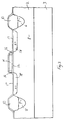
- Figures 1-5 represent the p-well of a CMOS integrated circuit in which n-channel transistors are fabricated.
- a layer 2 of p- type epitaxial silicon is initially formed on a p-type substrate 3.
- An oxide layer 4 is grown or deposited on the face of layer 2 to a depth of about 40 nanometers.
- a silicon nitride layer 6 is then deposited over layer 4 using low pressure chemical vapor deposition.
- Layers 4 and 6 are then patterned with photoresist and plasma etched to define the active region in layer 2 in which the field effect transistor will be formed. As a result of the patterning and etching step of layers 4 and 6, oxide/nitride layers 4 and 6 remain over the active region in layer 2. The areas in layer 2 where isolating thick field oxide will be subsequently be formed are exposed.
- a boron implant is then performed to create p- channel stop regions 8.
- the photoresist is then removed and thick field oxide regions 10 are thermally grown to a thickness of about 600-1000 nanometers.
- the remaining portions of layers 4 and 6 are then removed by etching to expose the face of layer 2.
- a gate oxide 12 is then thermally grown over the face of layer 2 between field oxide regions 10 to a thickness of about 10-40 nanometers.
- a layer of polysilicon is then deposited over layer 2 and doped N+ with an impurity such as phosphorous to render it conductive.
- the layer of polysilicon is then patterned with photoresist.
- a plasma etch removes the unprotected portion of the polysilicon layer to define conductive gate 14.
- An oxide layer is then deposited over layer 2 and anisotropically etched to form sidewall spacers 16. This etch also removes a portion of gate oxide 12 to expose the face of layer 2 between field oxide regions 10 and gate 14 as seen in Figure 2.
- a screen insulating layer 17 formed of oxide, nitride, or oxy-nitride, for example, and having a thickness of about 20-40 nanometers is then deposited or grown over layer 2.
- Screen insulating layer 17 prevents undesirable species, such as metal impurities, from reaching silicon layer 2 during source/drain implantation.
- the undesirable species have a lower energy than the species to be implanted during source/drain implantation and do not penetrate through screen insulating layer 17.
- Source/drain implants of a donor impurity such as arsenic, phosphorous, or antimony, are then performed using sidewall spacers 16 and gate 14 as a mask to create implanted source/drain regions 18.
- the source/drain implantation heavily damages the silicon in source/drain regions 18 and in many cases causes the silicon to be amorphized.
- An anneal is subsequently performed in either a furnace tube or in a single wafer rapid thermal annealer to electrically activate the source/drain impurity.
- the silicon damaged by implantation undergoes recrystallization.
- the recrystallization rate depends on crystallographic direction and proceeds fastest for (100) and (110) planes. These planes are often aligned along the edge of an implanted region for typical integrated circuit layouts.
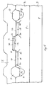
- Figure 4 shows the (100) and (110) planes aligned along the edges of implanted source/drain regions 18.
- Dislocations 20 and 22 may propagate into extend dislocations by the application of stress from overlayers or by subsequent processing.
- silicide layers 30 are formed by depositing a thin film of material such as Ti or Co, on the surface of layer 2 and reacting that material to form silicide layers 30 over source/drain regions 18 and gate 14.
- a poly-metal dielectric deposition (PMD) layer 24 is then deposited on layer 2, as shown in Figure 5, to provide insulation between gate 14 and source/drain regions 18 and a subsequently applied metal layer (not shown). Fabrication of PMD layer 24 involves high stress and high temperature and is an example of a processing step that can cause incipient damage areas, such as dislocations 20 and 22, to propagate into extended dislocations. Conventionally, PMD layer 24 is formed by low pressure chemical vapor deposition (LPCVD) at temperatures as high as 700 degrees Centigrade. The fabrication of PMD layer 24 by conventional LPCVD techniques produces high stress in layer 2 especially at gate edges and field oxide edges. The high stress at gate and field oxide edges can cause dislocations 20 and 22 to propagate into extended dislocations 32 and 34 as shown in Figure 5. Extended dislocations 32 and 34 may traverse distances as long as several microns.
- LPCVD low pressure chemical vapor deposition
- Extended dislocations 32 and 34 may become electrically active to provide a path for undesirable leakage currents that can render a circuit defective. Extended dislocations that become electrically active during manufacturing and testing are therefore a cause of yield loss. Extended dislocations that become electrically active in use subsequent to testing cause concern with regard to device reliability.
- the fabrication of a field effect transistor according to the method of the invention will now be described. Initially, the same steps discussed with respect to Figures 1-3 are performed to produce the structure of Figure 3.
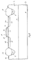
- the screen insulating layer 17 is then removed by either a wet chemical or plasma etch to expose the surface of source/drain regions 18 as shown in Figure 5. The removal step is performed after the source/drain implants but before the source/drain anneal.
- a thin native oxide (SiO2) layer 36 approximately 1-2 nanometers thick then grows on the exposed surfaces of source/drain regions 18 by exposure to air.
- This oxide layer 36 may grow in thickness to up to 4 nanometers thick during subsequent conventional chemical treatments, such as those used to remove particulate contamination.
- a source/drain anneal is then performed in a non-oxidizing atmosphere, such as nitrogen.
- a suitable annealing process using nitrogen the structure of Figure 6 is placed in a furnace chamber having a nitrogen ambient at between 450-700 degrees Centigrade for 30-120 minutes. The temperature is then ramped up to 900 degrees Centigrade at a rate of about 10 degrees Centigrade per minute in a nitrogen ambient.
- the furnace When the temperature reaches 900 degrees Centigrade during ramp up, the furnace is held at 900 degrees Centigrade in nitrogen for 20-60 minutes. The temperature is then ramped down to 800 degrees Centigrade at a rate of about 3 degrees Centigrade per minute in a nitrogen atmosphere. When the temperature reaches 800 degrees Centigrade the structure of Figure 6 is removed from the furnace.
- the anneal process may use other annealing schedules and may also take place in non-oxidizing atmospheres other than nitrogen, such as argon or vacuum. Rapid thermal annealing may also be used instead of furnace annealing.
- the vapor pressure of SiO causes the volatilization of SiO gas from the surface of native oxide layer 36 causing layer 36 to become silicon deficient.
- the subsequent tendency for silicon in source/drain regions 18 at the silicon-silicon dioxide interface between source/drain regions 18 and layer 36 to react with the oxygen-rich silicon dioxide in layer 36 provides a driving force to increase the concentration of silicon lattice vacancies in implanted source/drain regions 18. These silicon lattice vacancies are then able to diffuse into implant-damaged areas in source/drain regions 18 to counteract implant recrystallization damage.
- dislocations such as dislocations 20 and 22 in Figure 4
- a thin film of material such as Ti or Co, is then deposited on the surface of layer 2 and reacted to form silicide layers 30 over source/drain regions 18 and gate 14.
- a poly-metal dielectric deposition (PMD) layer 24 is then deposited on layer 2, as shown in Figure 7, to provide insulation between gate 14 and source/drain regions 18 and a subsequently applied metal layer (not shown). Since residual implant recrystallization damage during anneal is substantially reduced by the diffusion of silicon lattice vacancies into damaged areas, the likelihood that extended dislocations, such as extended dislocations 32 and 34 of Figure 5, will occur as a result of the stress introduced by layer 24 or other subsequent processing is also substantially reduced.
- Dislocation densities in source/drain regions in the p-wells at the edge of field oxide were determined for devices fabricated according to the invention and for devices fabricated according to the prior art method described in Figures 1-5.
- the dislocation density resulting from using the process of the invention was half that resulting from using the prior art method.
- An advantage of the invention is the reduction of residual recrystallization damage during anneal of implanted silicon and, as a result, a reduction in dislocation density.
- the reduction in dislocation density translates into an increase in manufacturing yield and an increase in reliability.
- the method can be used to fabricate an FET directly in the face of a substrate instead of in the face of an epitaxial layer or when fabricating an FET of the opposite conductivity type as in the case of a p-channel transistor of a CMOS integrated circuit.
- the process of the invention can be applied to any process that forms implanted regions in a semiconductor layer through a screen insulating layer, such as emitter/collector contact formation in bipolar transistor fabrication or buried bitline formation in memory device fabrication.
- the process is also applicable to semiconductor materials other than silicon in which an implanted region is damaged by the implant.
Landscapes
- Insulated Gate Type Field-Effect Transistor (AREA)
- Metal-Oxide And Bipolar Metal-Oxide Semiconductor Integrated Circuits (AREA)
Applications Claiming Priority (1)
| Application Number | Priority Date | Filing Date | Title |
|---|---|---|---|
| US4990893A | 1993-04-20 | 1993-04-20 |
Publications (2)
| Publication Number | Publication Date |
|---|---|
| EP0621629A2 true EP0621629A2 (de) | 1994-10-26 |
| EP0621629A3 EP0621629A3 (de) | 1996-07-17 |
Family
ID=21962393
Family Applications (1)
| Application Number | Title | Priority Date | Filing Date |
|---|---|---|---|
| EP94105613A Withdrawn EP0621629A3 (de) | 1993-04-20 | 1994-04-12 | Verfahren zur Reduzierung von den Vernetzungsfehlern in integrierte Schaltungbauelementen. |
Country Status (1)
| Country | Link |
|---|---|
| EP (1) | EP0621629A3 (de) |
Cited By (1)
| Publication number | Priority date | Publication date | Assignee | Title |
|---|---|---|---|---|
| US20140353733A1 (en) * | 2013-06-04 | 2014-12-04 | Global Foundries Inc. | Protection of the gate stack encapsulation |
Family Cites Families (4)
| Publication number | Priority date | Publication date | Assignee | Title |
|---|---|---|---|---|
| US5348900A (en) * | 1991-10-11 | 1994-09-20 | Sharp Kabushiki Kaisha | Process for manufacturing a semiconductor device including heat treatment in ammonia or oxygen |
| JP2763216B2 (ja) * | 1991-11-01 | 1998-06-11 | シャープ株式会社 | 半導体装置の製造方法 |
| JP2716300B2 (ja) * | 1991-10-11 | 1998-02-18 | シャープ株式会社 | 半導体装置の製造方法 |
| JP2771066B2 (ja) * | 1992-02-03 | 1998-07-02 | シャープ株式会社 | 半導体装置の製造方法 |
-
1994
- 1994-04-12 EP EP94105613A patent/EP0621629A3/de not_active Withdrawn
Cited By (1)
| Publication number | Priority date | Publication date | Assignee | Title |
|---|---|---|---|---|
| US20140353733A1 (en) * | 2013-06-04 | 2014-12-04 | Global Foundries Inc. | Protection of the gate stack encapsulation |
Also Published As
| Publication number | Publication date |
|---|---|
| EP0621629A3 (de) | 1996-07-17 |
Similar Documents
| Publication | Publication Date | Title |
|---|---|---|
| US5244819A (en) | Method to getter contamination in semiconductor devices | |
| US6037238A (en) | Process to reduce defect formation occurring during shallow trench isolation formation | |
| JP4066574B2 (ja) | 半導体装置の製造方法 | |
| US6933201B2 (en) | Method for manufacturing semiconductor device | |
| EP0631308A2 (de) | Verfahren zum Steuern der Dicke des Gate-Oxyds für die Herstellung von Halbleiterbauelementen | |
| US6900092B2 (en) | Surface engineering to prevent epi growth on gate poly during selective epi processing | |
| KR0129125B1 (ko) | 반도체 소자의 ldd mosfet 제조방법 | |
| US5637529A (en) | Method for forming element isolation insulating film of semiconductor device | |
| JP2856157B2 (ja) | 半導体装置の製造方法 | |
| US5795809A (en) | Semiconductor wafer fabrication process including gettering utilizing a combined oxidation technique | |
| WO2000034548A1 (en) | Multiple-thickness gate oxide formed by oxygen implantation | |
| US6670259B1 (en) | Inert atom implantation method for SOI gettering | |
| US5576230A (en) | Method of fabrication of a semiconductor device having a tapered implanted region | |
| US5631178A (en) | Method for forming a stable semiconductor device having an arsenic doped ROM portion | |
| KR100405015B1 (ko) | 반도체 장치의 제조 방법 | |
| JPH09167804A (ja) | 半導体装置及びその製造方法 | |
| US5950096A (en) | Process for improving device yield in integrated circuit fabrication | |
| US5763316A (en) | Substrate isolation process to minimize junction leakage | |
| US6069059A (en) | Well-drive anneal technique using preplacement of nitride films for enhanced field isolation | |
| US20040115889A1 (en) | Ultra shallow junction formation | |
| JP3382092B2 (ja) | 半導体装置の製造方法及び半導体装置 | |
| US5635752A (en) | Semiconductor device having source and drain regions which include horizontally extending secondary defect layers | |
| JPH10214844A (ja) | 半導体基板の製造方法 | |
| KR100291276B1 (ko) | 반도체 소자의 실리사이드 형성 방법 | |
| GB2307790A (en) | Method of removing defects from semiconductor devices. |
Legal Events
| Date | Code | Title | Description |
|---|---|---|---|
| PUAI | Public reference made under article 153(3) epc to a published international application that has entered the european phase |
Free format text: ORIGINAL CODE: 0009012 |
|
| AK | Designated contracting states |
Kind code of ref document: A2 Designated state(s): DE FR GB IT NL |
|
| PUAL | Search report despatched |
Free format text: ORIGINAL CODE: 0009013 |
|
| AK | Designated contracting states |
Kind code of ref document: A3 Designated state(s): DE FR GB IT NL |
|
| STAA | Information on the status of an ep patent application or granted ep patent |
Free format text: STATUS: THE APPLICATION IS DEEMED TO BE WITHDRAWN |
|
| 18D | Application deemed to be withdrawn |
Effective date: 19970118 |