EP0620656A2 - Emetteur-récepteur pour haute-fréquences - Google Patents
Emetteur-récepteur pour haute-fréquences Download PDFInfo
- Publication number
- EP0620656A2 EP0620656A2 EP94104893A EP94104893A EP0620656A2 EP 0620656 A2 EP0620656 A2 EP 0620656A2 EP 94104893 A EP94104893 A EP 94104893A EP 94104893 A EP94104893 A EP 94104893A EP 0620656 A2 EP0620656 A2 EP 0620656A2
- Authority
- EP
- European Patent Office
- Prior art keywords
- switched
- intermediate frequency
- signal
- oscillator
- frequency oscillator
- Prior art date
- Legal status (The legal status is an assumption and is not a legal conclusion. Google has not performed a legal analysis and makes no representation as to the accuracy of the status listed.)
- Granted
Links
- 238000001514 detection method Methods 0.000 claims description 18
- 230000005540 biological transmission Effects 0.000 claims description 13
- 238000011144 upstream manufacturing Methods 0.000 claims description 3
- 230000006978 adaptation Effects 0.000 description 2
- 230000010355 oscillation Effects 0.000 description 2
- 239000000872 buffer Substances 0.000 description 1
- 239000003990 capacitor Substances 0.000 description 1
- 239000007795 chemical reaction product Substances 0.000 description 1
- 238000010586 diagram Methods 0.000 description 1
- 230000010354 integration Effects 0.000 description 1
- 230000004048 modification Effects 0.000 description 1
- 238000012986 modification Methods 0.000 description 1
- 230000010363 phase shift Effects 0.000 description 1
- 239000000047 product Substances 0.000 description 1
- 230000035945 sensitivity Effects 0.000 description 1
Images

Classifications
-
- H—ELECTRICITY
- H04—ELECTRIC COMMUNICATION TECHNIQUE
- H04B—TRANSMISSION
- H04B1/00—Details of transmission systems, not covered by a single one of groups H04B3/00 - H04B13/00; Details of transmission systems not characterised by the medium used for transmission
- H04B1/38—Transceivers, i.e. devices in which transmitter and receiver form a structural unit and in which at least one part is used for functions of transmitting and receiving
- H04B1/40—Circuits
Definitions
- the invention relates to a transmitter / receiver arrangement for higher frequencies, in particular for applications in the mobile radio sector.
- the object of the invention is therefore to provide an integrable transmitter / receiver arrangement for higher frequencies, which is suitable for different circuit concepts.
- a transmitter / receiver arrangement with a reception branch mixer, which has a reception signal and multiplies a carrier frequency signal with one another, with a controlled first intermediate frequency oscillator which can be switched off by a switching signal and whose frequency range can be switched over by a first range control signal, with a demodulator connected downstream of the receiving branch mixer, to which the output signal of the first intermediate frequency oscillator is also fed directly and out of phase by 90 °, and the one Output signal, with a phase detection device connected downstream of the first intermediate frequency oscillator and in turn controlling it, the frequency range of which can be switched over by a second range control signal, with a controlled second intermediate frequency oscillator connected in parallel with the first intermediate frequency oscillator and which can be switched on by the switching control signal, with a transmission branch mixer, one input of which the outputs of the first and second intermediate frequency oscillator is connected and at the other input the carrier frequency signal is applied, and with a modulator connected downstream of the transmission branch mixer, to which an input signal is also fed and
- the arrangement according to the invention offers the user numerous adaptation options, the following three operating modes or circuit concepts preferably being selected.
- a first operating mode provides that the first intermediate frequency oscillator is switched on and the second intermediate frequency oscillator is switched off and that the first intermediate frequency oscillator and the phase detection device are switched in the same frequency range.
- the first intermediate frequency oscillator is also switched on and the second intermediate frequency oscillator is switched off.
- the first intermediate frequency oscillator and the phase detection device are switched between different frequency ranges.
- the first intermediate frequency oscillator is switched off and the second intermediate frequency oscillator is switched on during transmit mode, while the second intermediate frequency oscillator is switched off and the first intermediate frequency oscillator is switched on in reception mode.
- the first and second intermediate frequency oscillators have different frequency ranges, the phase detection device being switched to the frequency range of the second intermediate frequency oscillator in transmit mode and to the frequency range of the first intermediate frequency oscillator in receive mode.
- the phase detection device is provided by a phase detector with an upstream frequency divider, the divider ratio of which can be switched over via the second range control signal.
- the carrier frequency signal is generated by a controllable oscillator.
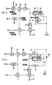
- the transmitter / receiver arrangement according to FIG. 1 contains a receive branch mixer 1, to which a receive signal 2 and a carrier frequency signal 3 are supplied.
- the receiving branch mixer 1 forms the product of the received signal 2 and the carrier frequency signal 3 and forwards this to a demodulation unit 4, which is also supplied with the output signal of a controllable oscillator 5 directly and out of phase by 90 ° and which outputs an output signal 17.
- the phase shift is generated by means of a phase shifter 6.
- phase-shifted signals can, however, also be generated in the same way, for example, by the controllable oscillator 5 itself.
- the frequency of the oscillator 5 is controlled by a phase detector 7 within a certain frequency range. This frequency range can be changed by a range control signal 8. In addition, the oscillator 5 can be switched off by means of a switching control signal 9.
- the frequency range of the phase detection device 7, the input of which is connected to the output of the oscillator 5, can also be switched by means of a range control signal 10.
- a controlled oscillator 11 is connected in parallel to the oscillator 5 and can be switched on by the switching control signal 9. Since only one of the two oscillators 5 and 11 should always be in operation, an inverter 12 is connected between the corresponding inputs for the switching control signal 9.
- the outputs of the oscillators 5 and 11 are at an input of a Transmitted branch mixer 13, which is additionally controlled by the carrier frequency signal 3.
- the transmit branch mixer is followed by a modulator 14, to which an input signal 15 is additionally applied for modulation and which emits a transmit signal 16.
- the arrangement shown can be fully or partially integrated, and it is also advantageous to divide it into two separate integrated circuits.
- the user is able to use several different circuit concepts, three of which are preferred circuit principles (operating modes). In the operating modes shown below, an application is assumed in which the transmit signal is in the range between 880 and 915 MHz and the receive signal in the range between 925 and 960 MHz.
- a phase shifter is used, the mutually phase-shifted output signals of which have half the frequency of the input signal.
- a frequency divider with the divider ratio 1: 2 is connected upstream of the transmission branch mixer 13 and the frequency of the oscillator 5 and 11 is doubled.
- the phase detection unit 7 consists of a phase detector PD 'operating at a fixed frequency, which is preceded by a divider with a switchable divider ratio.
- the carrier frequency signal 3 is generated by a controlled carrier frequency oscillator 20.
- FIGS. 2 to 4 of the drawings described below the same elements are provided with the same reference numerals, and units that are not in operation in the respective operating mode are not and alternately switched units are shown with dashed lines.
- an oscillator 20 with a large tuning range from 1126 to 1206 MHz is required, but only one of the two oscillators 5 and 11 is in operation, as a result of which a lower current consumption is achieved.
- the oscillator 5 In the operating mode according to FIG 3, only the oscillator 5 is also switched on.
- the oscillator 5 and the phase detection unit 7 are switched between two frequency ranges, for example between the fixed frequencies 400 MHz and 492 MHz, in accordance with the transmission and reception mode.
- the circuit structure essentially corresponds to that according to FIG. 2. In contrast to this, however, the oscillator 5 and the phase detection unit 7 are switched between the named ranges.
- the carrier frequency oscillator advantageously works at a low oscillation frequency and over a small tuning range from 679 to 715 MHz. In this operating mode too, only two oscillators, namely the oscillator 5 and the oscillator 20, are in operation. Power consumption is also low.
- the oscillator 11 In the operating mode according to FIG. 4, the oscillator 11 is switched on in the transmission mode and the oscillator 5 is switched off. Conversely, in reception mode, the oscillator 11 is switched off and the oscillator 5 is switched on.
- the oscillators 5 and 11 work in different frequency ranges. For example, the oscillator 11 operates in transmission mode at 400 MHz and the oscillator 5 in reception mode at 492 MHz.
- the phase detection unit 7 therefore operates in the transmit mode at the frequency of the oscillator 11, that is to say at approximately 400 MHz, and in receive mode at the frequency of the oscillator 5, that is to say at approximately 492 MHz.
- the switching of the phase detection unit 7 and the switching on and off of the oscillators 5 and 11 takes place with the control signals 10 and 9.
- the carrier frequency oscillator 20 in turn operates at a low oscillation frequency in the range between 679 and 715 MHz and has a small tuning range. Since the oscillators 5 and 11 are switched on alternately, that is to say only ever one of the two is in operation, lower power consumption is again achieved.
- the modulator 14, the transmission branch mixer 13, possibly the divider 18, the controlled oscillator 11, the phase detection unit 7 and possibly the carrier frequency oscillator 20 are preferably integrated in a circuit, while the reception branch mixer 1, the demodulator 4, the controlled oscillator 5 and possibly the phase shifter 6 will be integrated in another circuit.
- frequency-determining elements such as inductors and capacitors are designed as discrete elements. This enables an extremely flexible system architecture in the presented transceiver arrangement. As has been shown, at least three different operating variants can be implemented without the need to modify the circuits on the chip. This is done by a single one in the Frequency switchable phase detection unit achieved in conjunction with a controlled oscillator also switchable in frequency.
- a further controlled oscillator is provided, which can optionally be used instead of the switchable oscillator.
- All controlled oscillators are designed in such a way that they can be operated either with the aid of external passive components as oscillators or as input buffers for signals which are generated by external oscillators.
- the arrangement according to the invention offers the user the advantage of a highly flexible system architecture. This does not have to commit to a concept from the outset, but can weigh up the advantages and disadvantages of the various concepts and then decide individually.
Landscapes
- Engineering & Computer Science (AREA)
- Computer Networks & Wireless Communication (AREA)
- Signal Processing (AREA)
- Transceivers (AREA)
- Superheterodyne Receivers (AREA)
Applications Claiming Priority (2)
| Application Number | Priority Date | Filing Date | Title |
|---|---|---|---|
| DE4312020 | 1993-04-13 | ||
| DE4312020 | 1993-04-13 |
Publications (3)
| Publication Number | Publication Date |
|---|---|
| EP0620656A2 true EP0620656A2 (fr) | 1994-10-19 |
| EP0620656A3 EP0620656A3 (fr) | 1994-12-14 |
| EP0620656B1 EP0620656B1 (fr) | 1999-07-07 |
Family
ID=6485358
Family Applications (1)
| Application Number | Title | Priority Date | Filing Date |
|---|---|---|---|
| EP94104893A Expired - Lifetime EP0620656B1 (fr) | 1993-04-13 | 1994-03-28 | Emetteur-récepteur pour haute-fréquences |
Country Status (3)
| Country | Link |
|---|---|
| US (1) | US5566360A (fr) |
| EP (1) | EP0620656B1 (fr) |
| DE (1) | DE59408452D1 (fr) |
Families Citing this family (1)
| Publication number | Priority date | Publication date | Assignee | Title |
|---|---|---|---|---|
| JPH08186519A (ja) * | 1994-12-27 | 1996-07-16 | Sony Corp | 送受信回路 |
Family Cites Families (14)
| Publication number | Priority date | Publication date | Assignee | Title |
|---|---|---|---|---|
| US1584623A (en) * | 1920-04-23 | 1926-05-11 | Westinghouse Electric & Mfg Co | Switchboard |
| JPS51117510A (en) * | 1975-04-07 | 1976-10-15 | Shintou Denki Kk | Double superheterodyne receiver |
| GB1584622A (en) * | 1976-08-02 | 1981-02-18 | Motorola Inc | Multichannel communication device with manual and automatic scanning electronic channel selection |
| JPS54139316A (en) * | 1978-04-20 | 1979-10-29 | Matsushita Electric Ind Co Ltd | Am ssb transmitter/receiver |
| JPS5689136A (en) * | 1979-12-21 | 1981-07-20 | Toshiba Corp | Transmitter-receiver of press-to-talk system |
| JPS58123642U (ja) * | 1982-02-17 | 1983-08-23 | 株式会社ケンウッド | トランシ−バ |
| JPS61294936A (ja) * | 1985-06-21 | 1986-12-25 | Nec Corp | シンセサイザ− |
| FI81933C (fi) * | 1989-05-18 | 1990-12-10 | Nokia Mobira Oy | Foerfarande foer alstring av frekvenser i en digital radiotelefon. |
| JPH04160926A (ja) * | 1990-10-25 | 1992-06-04 | Sony Corp | 送受信装置 |
| JP2850160B2 (ja) * | 1991-01-25 | 1999-01-27 | 松下電器産業株式会社 | 時分割複信無線送受信装置 |
| KR940007469B1 (ko) * | 1991-05-23 | 1994-08-18 | 삼성전자 주식회사 | 이동 무선전화기에 있어서 주파수 소스회로 |
| JP2998296B2 (ja) * | 1991-05-31 | 2000-01-11 | 日本電気株式会社 | ディジタル無線通信装置 |
| FI91819C (fi) * | 1991-11-05 | 1994-08-10 | Nokia Mobile Phones Ltd | Menetelmä kahden eri taajuusalueella toimivan digitaalisen radiopuhelimen taajuuksien muodostamiseksi |
| US5390363A (en) * | 1993-04-30 | 1995-02-14 | Motorola, Inc. | Transmitter and receiver circuit and method therefor |
-
1994
- 1994-03-28 EP EP94104893A patent/EP0620656B1/fr not_active Expired - Lifetime
- 1994-03-28 DE DE59408452T patent/DE59408452D1/de not_active Expired - Lifetime
- 1994-04-13 US US08/226,967 patent/US5566360A/en not_active Expired - Lifetime
Non-Patent Citations (1)
| Title |
|---|
| None |
Also Published As
| Publication number | Publication date |
|---|---|
| EP0620656A3 (fr) | 1994-12-14 |
| US5566360A (en) | 1996-10-15 |
| EP0620656B1 (fr) | 1999-07-07 |
| DE59408452D1 (de) | 1999-08-12 |
Similar Documents
| Publication | Publication Date | Title |
|---|---|---|
| DE69736793T2 (de) | Verfahren zum Erzeugen von Frequenzen in einem Sender-Empfänger mit direkter Umwandlung eines Dualband-Radiokommunikationssystems, ein Sender-Empfänger mit direkter Umwandlung eines Dualband-Radiokommunikationssystems und die Verwendung dieses Verfahrens und dieser Vorrichtung in einer mobilen Station | |
| DE3913593C2 (de) | Schaltungsanordnung zur Umsetzung eines empfangenen modulierten Informationssignals in ein Zwischenfrequenzsignal | |
| DE69515336T2 (de) | Mischer mit spiegelfrequenz-unterdrückung | |
| DE69837698T2 (de) | Multimodusfunkkommunikationssystem | |
| DE69737000T2 (de) | Funksender Empfänger für Senden und Empfang von MF Signalen in zwei Bändern | |
| DE69623426T2 (de) | Multimoden-Funkendgerät | |
| DE69637274T2 (de) | TDMA-Funkgerätschaltung mit variablem zweiten Lokaloszillator | |
| DE102007023795A1 (de) | Oszillator zum Erzeugen von unterschiedlichen Schwingungen | |
| DE60018440T2 (de) | Überlagerungsoszillator für hochfrequenzfunkgeräte | |
| DE3903262C2 (fr) | ||
| EP1163727A1 (fr) | Synthetiseur de frequence | |
| DE19928998B4 (de) | Elektronische Schaltungsanordnung zur Erzeugung einer Sendefrequenz | |
| EP1102392B1 (fr) | Modulateur en quadrature | |
| DE3123973C2 (de) | Phasenregelschaltung | |
| DE69801358T2 (de) | Frequenzwandlerschaltung für Kabelempfänger mit Modem | |
| DE2442985C2 (fr) | ||
| DE3046540A1 (de) | Phasenregelkreis | |
| DE3240565A1 (de) | Direktmischender synchronempfaenger | |
| EP1258077B1 (fr) | Ensemble circuit de modulation directe | |
| EP0552642B1 (fr) | Radioémetteur et -récepteur avec circuit à bande de verrouillage de phase | |
| DE69222279T2 (de) | TDMA-TDD Sender-Empfänger | |
| DE3200560C2 (fr) | ||
| EP0620656B1 (fr) | Emetteur-récepteur pour haute-fréquences | |
| DE19823103C2 (de) | Mehrfachband-Frequenzgenerierung mit einer PLL-Schaltung | |
| DE60033762T2 (de) | Verbrauchsarmer mehrfrequenzoszillator für telekommunikations-ic's |
Legal Events
| Date | Code | Title | Description |
|---|---|---|---|
| PUAI | Public reference made under article 153(3) epc to a published international application that has entered the european phase |
Free format text: ORIGINAL CODE: 0009012 |
|
| AK | Designated contracting states |
Kind code of ref document: A2 Designated state(s): DE FR GB IT NL |
|
| PUAL | Search report despatched |
Free format text: ORIGINAL CODE: 0009013 |
|
| AK | Designated contracting states |
Kind code of ref document: A3 Designated state(s): DE FR GB IT NL |
|
| 17P | Request for examination filed |
Effective date: 19950103 |
|
| 17Q | First examination report despatched |
Effective date: 19980511 |
|
| GRAG | Despatch of communication of intention to grant |
Free format text: ORIGINAL CODE: EPIDOS AGRA |
|
| GRAG | Despatch of communication of intention to grant |
Free format text: ORIGINAL CODE: EPIDOS AGRA |
|
| GRAH | Despatch of communication of intention to grant a patent |
Free format text: ORIGINAL CODE: EPIDOS IGRA |
|
| GRAH | Despatch of communication of intention to grant a patent |
Free format text: ORIGINAL CODE: EPIDOS IGRA |
|
| GRAA | (expected) grant |
Free format text: ORIGINAL CODE: 0009210 |
|
| AK | Designated contracting states |
Kind code of ref document: B1 Designated state(s): DE FR GB IT NL |
|
| REF | Corresponds to: |
Ref document number: 59408452 Country of ref document: DE Date of ref document: 19990812 |
|
| ET | Fr: translation filed | ||
| ITF | It: translation for a ep patent filed | ||
| GBT | Gb: translation of ep patent filed (gb section 77(6)(a)/1977) |
Effective date: 19990909 |
|
| PLBE | No opposition filed within time limit |
Free format text: ORIGINAL CODE: 0009261 |
|
| STAA | Information on the status of an ep patent application or granted ep patent |
Free format text: STATUS: NO OPPOSITION FILED WITHIN TIME LIMIT |
|
| 26N | No opposition filed | ||
| REG | Reference to a national code |
Ref country code: GB Ref legal event code: IF02 |
|
| PGFP | Annual fee paid to national office [announced via postgrant information from national office to epo] |
Ref country code: NL Payment date: 20040227 Year of fee payment: 11 |
|
| PG25 | Lapsed in a contracting state [announced via postgrant information from national office to epo] |
Ref country code: IT Free format text: LAPSE BECAUSE OF NON-PAYMENT OF DUE FEES;WARNING: LAPSES OF ITALIAN PATENTS WITH EFFECTIVE DATE BEFORE 2007 MAY HAVE OCCURRED AT ANY TIME BEFORE 2007. THE CORRECT EFFECTIVE DATE MAY BE DIFFERENT FROM THE ONE RECORDED. Effective date: 20050328 |
|
| PG25 | Lapsed in a contracting state [announced via postgrant information from national office to epo] |
Ref country code: NL Free format text: LAPSE BECAUSE OF NON-PAYMENT OF DUE FEES Effective date: 20051001 |
|
| NLV4 | Nl: lapsed or anulled due to non-payment of the annual fee |
Effective date: 20051001 |
|
| REG | Reference to a national code |
Ref country code: GB Ref legal event code: 732E Free format text: REGISTERED BETWEEN 20110707 AND 20110713 |
|
| REG | Reference to a national code |
Ref country code: FR Ref legal event code: TP Owner name: INFINEON TECHNOLOGIES AG, DE Effective date: 20110922 |
|
| REG | Reference to a national code |
Ref country code: DE Ref legal event code: R081 Ref document number: 59408452 Country of ref document: DE Owner name: INTEL MOBILE COMMUNICATIONS GMBH, DE Free format text: FORMER OWNER: SIEMENS AKTIENGESELLSCHAFT, 80333 MUENCHEN, DE Effective date: 20111107 Ref country code: DE Ref legal event code: R081 Ref document number: 59408452 Country of ref document: DE Owner name: INTEL MOBILE COMMUNICATIONS TECHNOLOGY GMBH, DE Free format text: FORMER OWNER: SIEMENS AKTIENGESELLSCHAFT, 80333 MUENCHEN, DE Effective date: 20111107 |
|
| REG | Reference to a national code |
Ref country code: FR Ref legal event code: TP Owner name: INTEL MOBILE COMMUNICATIONS GMBH, DE Effective date: 20120404 |
|
| REG | Reference to a national code |
Ref country code: GB Ref legal event code: 732E Free format text: REGISTERED BETWEEN 20121213 AND 20121219 |
|
| PGFP | Annual fee paid to national office [announced via postgrant information from national office to epo] |
Ref country code: GB Payment date: 20130327 Year of fee payment: 20 Ref country code: DE Payment date: 20130320 Year of fee payment: 20 Ref country code: FR Payment date: 20130325 Year of fee payment: 20 |
|
| REG | Reference to a national code |
Ref country code: DE Ref legal event code: R081 Ref document number: 59408452 Country of ref document: DE Owner name: INTEL MOBILE COMMUNICATIONS GMBH, DE Free format text: FORMER OWNER: INTEL MOBILE COMMUNICATIONS GMBH, 85579 NEUBIBERG, DE Effective date: 20130315 Ref country code: DE Ref legal event code: R081 Ref document number: 59408452 Country of ref document: DE Owner name: INTEL MOBILE COMMUNICATIONS GMBH, DE Free format text: FORMER OWNER: INTEL MOBILE COMMUNICATIONS TECHNOLOGY GMBH, 85579 NEUBIBERG, DE Effective date: 20130326 Ref country code: DE Ref legal event code: R081 Ref document number: 59408452 Country of ref document: DE Owner name: INTEL MOBILE COMMUNICATIONS GMBH, DE Free format text: FORMER OWNER: INFINEON TECHNOLOGIES AG, 85579 NEUBIBERG, DE Effective date: 20130315 Ref country code: DE Ref legal event code: R081 Ref document number: 59408452 Country of ref document: DE Owner name: INTEL MOBILE COMMUNICATIONS GMBH, DE Free format text: FORMER OWNER: INFINEON TECHNOLOGIES AG, 85579 NEUBIBERG, DE Effective date: 20130314 |
|
| REG | Reference to a national code |
Ref country code: GB Ref legal event code: 732E Free format text: REGISTERED BETWEEN 20131017 AND 20131023 |
|
| REG | Reference to a national code |
Ref country code: DE Ref legal event code: R071 Ref document number: 59408452 Country of ref document: DE |
|
| REG | Reference to a national code |
Ref country code: GB Ref legal event code: PE20 Expiry date: 20140327 |
|
| PG25 | Lapsed in a contracting state [announced via postgrant information from national office to epo] |
Ref country code: DE Free format text: LAPSE BECAUSE OF EXPIRATION OF PROTECTION Effective date: 20140329 Ref country code: GB Free format text: LAPSE BECAUSE OF EXPIRATION OF PROTECTION Effective date: 20140327 |