EP0618575B1 - Verfahren und Vorrichtung zum Formatieren eines einmalig beschreibbaren Informationsmediums - Google Patents
Verfahren und Vorrichtung zum Formatieren eines einmalig beschreibbaren Informationsmediums Download PDFInfo
- Publication number
- EP0618575B1 EP0618575B1 EP94302161A EP94302161A EP0618575B1 EP 0618575 B1 EP0618575 B1 EP 0618575B1 EP 94302161 A EP94302161 A EP 94302161A EP 94302161 A EP94302161 A EP 94302161A EP 0618575 B1 EP0618575 B1 EP 0618575B1
- Authority
- EP
- European Patent Office
- Prior art keywords
- bit
- data
- packet
- memory
- writing
- Prior art date
- Legal status (The legal status is an assumption and is not a legal conclusion. Google has not performed a legal analysis and makes no representation as to the accuracy of the status listed.)
- Expired - Lifetime
Links
Images

Classifications
-
- G—PHYSICS
- G11—INFORMATION STORAGE
- G11B—INFORMATION STORAGE BASED ON RELATIVE MOVEMENT BETWEEN RECORD CARRIER AND TRANSDUCER
- G11B11/00—Recording on or reproducing from the same record carrier wherein for these two operations the methods are covered by different main groups of groups G11B3/00 - G11B7/00 or by different subgroups of group G11B9/00; Record carriers therefor
-
- G—PHYSICS
- G11—INFORMATION STORAGE
- G11B—INFORMATION STORAGE BASED ON RELATIVE MOVEMENT BETWEEN RECORD CARRIER AND TRANSDUCER
- G11B20/00—Signal processing not specific to the method of recording or reproducing; Circuits therefor
- G11B20/10—Digital recording or reproducing
- G11B20/12—Formatting, e.g. arrangement of data block or words on the record carriers
- G11B20/1215—Formatting, e.g. arrangement of data block or words on the record carriers on cards
-
- G—PHYSICS
- G11—INFORMATION STORAGE
- G11B—INFORMATION STORAGE BASED ON RELATIVE MOVEMENT BETWEEN RECORD CARRIER AND TRANSDUCER
- G11B20/00—Signal processing not specific to the method of recording or reproducing; Circuits therefor
- G11B20/10—Digital recording or reproducing
- G11B20/18—Error detection or correction; Testing, e.g. of drop-outs
- G11B20/1806—Pulse code modulation systems for audio signals
- G11B20/1809—Pulse code modulation systems for audio signals by interleaving
Definitions
- the present invention generally relates to a write once type information recording medium such as an optical memory card. More specifically, the present invention is directed to a method and apparatus which is capable of formatting a write once type information recording medium with increasing storage efficiency, and which has the capability of correcting burst errors, to a write once type information recording medium formatted in accordance with the above-mentioned format, and to a method and apparatus for writing data to or reading data from such a write once type information recording medium.
- an error correction code is added to the data during a data recording operation so as to perform the error correction.
- error correction code There are typically two different types of errors occurring in the reproduced data, namely, random errors occurring at random, and burst errors occurring in a continuous manner. Once a burst error occurs, it can hardly be corrected owing to a large continuous errors included therein.
- interleaving is carried out in a conventional information recording system. That is, a series of data is subdivided into a large number of data segments which will then be distributed into the recording medium. In this case, even if positionally continuous errors occur on the recording medium due to defects thereof, the errors are not continued on the reproduced data. As a result, these errors can be corrected as random errors.
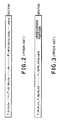
- Fig. 1 schematically represents an example of the conventional interleaving technique.
- 272 "synchronization signals for a frame and bit” (simply, referred to “synchronization signals”) are first arranged, each of which is composed of 8 bits, for instance, and indicated by symbol “F” as illustrated in Fig. 1.
- a 272-bit packet "a”, a 272-bit packet "b”, a 272-bit packet “c”, ---, a 272-bit packet "n” are arranged in parallel to each other, as illustrated in Fig. 1.
- the first 272-bit packet "a” contains 190-bit data consisting of a1, a2, ---, and a190, and an 82-bit error correction code consisting of a191, a192, ---, and a272.
- the second 272-bit packet “b” contains 190-bit data consisting of b1 to b190, and an 82-bit error correction code consisting of b191 to b272
- the third 272-bit packet “c” contains 190-bit data consisting of c1 to c190, and an 82-bit error correction code consisting of c191 to c272.
- the final 272-bit packet "n” contains 190-bit data consisting of n1 to n190, and an 82-bit error correction code consisting of n191 to n272.
- the 8-bit synchronization signals and the plurality of packets which have been arranged in the above-described manner, are read in the direction indicated by arrows shown in Fig. 3 as follows.
- the reading operation is carried out sequentially from the synchronization signal F, the first bit a1 of the first packet "a”, the first bit b1 of the second packet “b”, the first bit c1 of the third packet “c", and up to the first bit n1 of the last packet "n”.
- the reading operation is performed sequentially from the synchronization signal F, the second bit a2 of the first packet "a", the second bit b2 of the second packet "b", the second bit c2 of the third packet "c", and up to the second bit n2 of the final packet "n".
- the packets up to the 272-nd bit n272 of the last packet "n" are read out, and then they are rearranged as a bit stream as shown in Fig. 2. Conventionally, such a rearranged bit stream is recorded on the information recording medium.
- the bit stream, beginning from the synchronization signal "F" through a1 to n272, as shown in Fig. 2 is called a "sector".
- the larger the number of interleaving processes becomes namely, the greater the quantity of packets becomes
- the increasing number of interleaving processes requires a longer sector. Since various lengths of data are normally recorded in a single sector, a long sector may include a useless storage capacity in case of short (small) data.
- short data having three packets is stored into a long (large) sector. As shown in Fig.
- the conventional data recording medium posses a trade-off problem in that if a sector is set long, the useless unrecorded portion is increased, and therefore the recording efficiency is lowered, whereas if a sector is set short, the error correction capability is reduced.
- Another concern of the present invention is to provide a method and an apparatus capable of formatting a write once type recording medium, while optimizing storage efficiency and improving error correction capability.
- a further concern of the present invention is to provide a data writing/reading apparatus capable of writing data to and reading data from a write once type recording medium, while optimizing storage efficiency and improving error correction capability.
- EP-A-0520381 discloses an optical recording apparatus for use with a write once compact disc. Additional information in the form of a sub-code is added to the information to be recorded to constitute unitary frames. The addition of this sub-code information is done in such a way that when the recording of a unitary frame is interrupted half-way through the frame missing additional information is regenerated.
- United Kingdom Patent Specification No GB-A-2187008 discloses a method of storing digital information in which a double-symbol connecting code is used and which is interleaved in sectors of the stored data.
- European Patent Specification No EP-A-0342833 discloses apparatus for use with writing to and reproducing data from a compact disc.
- a predetermined error correction code is added to input data.
- the input data can be interleaved on recording in response to control address means in alternative ways so that either convolution encoding can be carried out or that the input data is interleaved in a format allowing computer encoding in a sector of the input data.
- a recording method for formatting a write once type recording medium as set out in claim 1.
- the synchronization signals are recorded with a predetermined interval, and the data are sequentially recorded bit by bit following the respective synchronization signals, thereby scattering data strings.
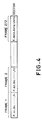
- a single sector is formed by serially arranging 272 pieces of 48-bit frames (generally, x pieces of frames with 48 bits).
- a 48-bit (generally, p bits) frame contains an 8-bit (generally, f bits) synchronization signal "F" placed at the leading portion, and maximum 40 bits (generally, p-f bits) of data and an error correction code following the synchronization signal "F".
- one sector is constructed of 48X272 bits (generally, px bits).
- Both the data and the error correction codes are recorded in such a memory region whose capacity is an integer multiple of the bit size of a single packet, where the integer is 1 - 40.
- a single packet includes 190-bit (generally , u-bit) data and an 82-bit (generally, v-bit) error correction code.
- bit "d1" of the fourth package is additionally written following to the bit c1 within the frame 1, which already has the synchronization signal "F".
- the other bits "d2", “d3", ---, "d272" of the fourth packed are successively written after the preceding bits "c2", "c3", --, "c272".
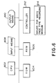
- Fig. 6 is a block diagram schematically showing a first embodiment of the hardware arrangement of an apparatus for formatting the above-described write once type recording medium of Fig. 4, according to the present invention.
- reference numeral 602 designates a CPU (central processing unit) for controlling the overall arrangement of this formatting apparatus.
- Reference numeral 604 denotes a ROM (read-only memory) for previously storing a program for executing an initializing process when the power supply (not shown) of the formatting apparatus is turned ON.
- Reference numeral 606 denotes a RAM (random access memory) for temporarily storing data required during the operation of the program.
- Reference numeral 608 denotes an input means for inputting instructions of the formatting operation, such as a keyboard, a mouse, and a communication device.
- Reference numeral 614 denotes a driver for a write once type information recording medium, which formats the write once type information recording medium, and for writing data to and reading data from this recording medium.
- Reference numeral 610 is an output means for outputting information to a user, such as a CRT (cathode-ray tube), an LCD (liquid crystal display), and a communication device.
- Reference numeral 612 denotes a controller for controlling the driver 614 for a write once type information recording medium in response to the instructions issued from the CPU 602.
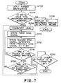
- step S702 of this flow chart the instruction for the formatting operation by the formatting apparatus is inputted.
- step S704 CPU 602 judges via the controller 612 whether or not a write once type information recording medium is inserted into the driver 614. If a write once type information recording medium is not inserted into the driver 614, this state is supplied to the output means 610 at step S706 and then the process terminates. On the other hand, when a write once type information recording medium is inserted into the driver 614, the CPU 602 instructs the controller 612 to move the head of the driver 614 to a predetermined track (S708).
- the first f-bit synchronization signal "F” is written to the starting position of a first sector on this track of the recording medium (S710). Furthermore, the second f-bit synchronization signal “F” is written into the position, which is adjacent to the first f-bit synchronization signal F and is separated by a p-bit data region (S712). The writing operation of the synchronization signal F is repeated until the synchronization signals F are written into the entire (x pieces of) frames in this sector which is being formatted (S714).
- the CPU 602 handles as a single sector the region from the starting position of the first synchronization signal to the end position of the p-bit data following the x-th synchronization signal. It should be noted that the sector number or the like may be written into the starting position of the respective sectors.
- the CPU 602 conforms that x pieces of synchronization signals F have been written into all of the sectors within this track (S750), the CPU 602 makes further judgment as to whether or not all of the desired tracks have been formatted (S760).
- the head of the diver 614 is transported to the succeeding track to commence the formatting operation of this track (from S708 to S750) under the control of the CPU 602. In contrast, when all of these desired tracks have been formatted, this process operation is completed (S760).
- FIG. 8 An embodiment of data reading/writing apparatus and a method for reading data form and writing data to the above-explained write once type information recording medium, in accordance with the present invention, will now be described with reference to Figs. 8 and 9.
- a hardware block diagram of this data reading/writing apparatus is identical to the above-explained hardware block diagram of the formatting apparatus shown in Fig. 6. It should be noticed, however, that in order to increase the data read and write speed, a data memory having a memory capacity corresponding to a single track, and a memory processing circuit may be employed in the controller 612 of the data reading/writing apparatus, which will be described in more detail.
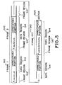
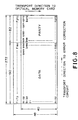
- Fig. 8 shows the memory map of a memory, which stores data contained in a single track.
- One code word in the row (horizontal) direction is composed of 272 bits, and 40 code words are arranged in the column (vertical) direction, one code word consisting of 190-bit data and an 82-bit error correction code.
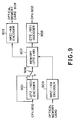
- Fig. 9 is a schematic block diagram of a memory processing circuit having the memory map shown in Fig. 8. This memory processing circuit performs recording and reproducing operations using an optical memory card as the write once type information recording medium.
- An encoder 901 produces error correction codes so that the data sent from CPU 602 are provided with the error correction codes, and then stored into a memory 902 in the form shown in Fig. 8.
- the row “a" (a1 to a272) shown in Fig. 8 is stored into the memory 902 as follows: First, a switch 906 is connected to the "a" side, and the data sent from CPU 602 are sequentially stored into the row "a" of the memory 902 as bits a1, a2, a3, ---, a190. Thereafter, the switch 906 is connected to the "b" side, and the 82-bit error correction code produced by the encoder 901 is supplied to the bits a191 - a272 of the memory 902.
- the data in the optical memory card have been stored by the above-described recording operation.
- the data read out from the optical memory card is decoded into a digital signal by a decoder 904.
- the digital signal is stored into the memory 902 in the vertical direction in such a manner that they are arranged in accordance with the memory map of Fig. 8.
- the data is retrieved from the memory 902 in the horizontal direction and is supplied to the decoder 905, and which processes the data in accordance with the error correction method.
- the error-corrected data is sent to the CPU 602 as reproduction data.
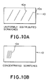
- the above-described data recording/reproducing methods can achieve the effective error correction not only when scratches 10a are made in the optical memory card 908 in a uniform distribution as illustrated in Fig. 10A, (in this case, error corrections are carried out even in the conventional recording format), but also when scratches 10a are concentratedly made at one place as shown in Fig. 10B,.
- the error correction capability will be considerably increased in the case of a short sector, as compared with the conventional error correction method.
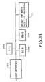
- Fig. 11 is a schematic block diagram showing a second embodiment of a hardware arrangement for a formatting apparatus and a data input/output device according to of the present invention.
- the second embodiment includes a host interface 1120 in accordance with SCSI or SASI which can be used as an input means and an output means instead of the input means 608 and the output means 610 of the formatting apparatus and the data input/output apparatus of the first embodiment.
- all or a part of the function of the controller 612 may be replaced by a CPU 1102, a ROM 1104, and a RAM 1106.
- the controller 612 may be interposed between a write once type recording medium driver 1114 and the CPU 1102.
- a communication interface with LAN (local area network), WAN (wide area network), or public network may be substituted for the host interface 1120, so that the interface is used as the input means and the output means.
- the bit storage efficiency to the frame can be increased. Also, the sector of a large size can be selected. As a consequence, the data recording efficiency and the error correction capability can be improved. Moreover, data can be additionally written on a sector without dividing it.
Claims (8)
- Verfahren zum Formatieren eines einmal beschreibbaren Aufzeichnungsmediums durch Bilden einer Vielzahl von Sektoren auf dem einmal beschreibbaren Aufzeichnungsmedium, wobei jeder der Vielzahl von Sektoren x p-Bit-Rahmen enthält, wobei jeder der p-Bit-Rahmen einen f-Bit-Synchronisationssignalbereich und einen d-Bit-Datenbereich enthält, umfassend die Schritte:Schreiben eines Synchronisationssignals in jeden der f-Bit-Synchronisationssignalbereiche gefolgt von dem d-Bit-Datenbereich;wobei x, p, f und d positive ganze Zahlen sind und p mit (f+d) übereinstimmt.
- Verfahren nach Anspruch 1, und umfassend:einen Speicherschritt des Speicherns von zumindest einem x-Bit-Paket, in dem ein v-Bit-Fehlerkorrekturcode zu u-Bit-Daten addiert ist, in einen Speicher; undeinen Datenschreibschritt des Schreibens der jeweiligen Bits des aus dem Speicher ausgelesenen Pakets in die Datenbereiche der x p-Bit-Rahmen;wobei x, p, f, d, u und v positive ganze Zahlen sind.
- Verfahren nach Anspruch 2, wobei der Speicherschritt umfaßt einen Schritt des Speicherns des zumindest einen Pakets in einer Vielzahl von Speichern; undwobei der Datenschreibschritt umfaßt einen Schritt des Schreibens eines n-ten Bits eines jeden Pakets in einen n-ten Rahmen;wobei n eine positive ganze Zahl kleiner oder gleich x ist.
- Verfahren nach Anspruch 3, wobei 272 als die Rahmennummer "x" für jeden der Sektoren gewählt wird;wobei 48 als die Bitnummer "p" des Rahmens gewählt wird;wobei 8 als die Bitnummer "f" des Synchronisiersignalbereichs gewählt wird; und wobei 40 als die Bitnummer "d" des Datenbereichs gewählt wird.
- Verfahren nach Anspruch 4, wobei 190 als die Bitnummer "u" der Daten gewählt wird; undwobei 82 als die Bitnummer "v" des Fehlerkorrekturcodes gewählt wird.
- Verfahren nach Anspruch 2 und einem der Ansprüche 4 oder 5, wenn diese vom Anspruch 3 abhängig sind, mit dem Schritt des bitweisen Lesens einer Information aus den in demSpeicher gespeicherten x Daten; unddes seriellen Verbindens der gelesenen Information zum Bilden eines x-Bit-Pakets.
- Vorrichtung zum Formatieren eines einmal beschreibbaren Aufzeichnungsmediums mit einem eine Vielzahl von Sektoren enthaltenden Format, wobei jeder der Sektoren x p-Bit-Rahmen enthält, die jeweils f-Bit-Synchronisationssignalbereiche und d-Bit-Datenbereiche enthalten, wobei die Vorrichtung umfaßt:ein ROM (Nur-Lese-Speicher) (604) zum Speichern eines Programms zum Durchführen eines Initialisierungsvorgangs der Vorrichtung beim Aktivieren der Vorrichtung;eine Eingabeeinrichtung (608) zum Eingeben einer Anweisung für eine Formatierungsoperation;einen Speicher (902) zum Speichern von zumindest einem x-Bit-Paket, in dem ein v-Bit-Fehlerkorrekturcode zu u-Bit-Daten addiert ist;eine Synchronisationssignalschreibeinrichtung (612, 614) zum Schreiben eines Synchronisationssignals in jeden der Synchronisationssignalbereiche, jeweils gefolgt von den d-Bit-Datenbereichen, in Übereinstimmung mit der Eingabeanweisung; undeine Ausgabeeinrichtung (610) zum Ausgeben einer die Fertigstellung der Formatierung anzeigenden Ausgabe, nachdem das einmal beschreibbare Aufzeichnungsmedium formatiert wurde; wobei x, p, f und d positive ganze Zahlen sind.
- Vorrichtung nach Anspruch 7, wobei 272 als die Rahmennummern "x" für jeden der Sektoren gewählt ist;wobei 48 als die Bitnummer "p" des Rahmens gewählt ist;wobei 8 als die Bitnummer "f" des Synchronisationssignalbereichs gewählt ist; undwobei 40 als die Bitnummer "d" des Datenbereichs gewählt ist.
Applications Claiming Priority (4)
| Application Number | Priority Date | Filing Date | Title |
|---|---|---|---|
| JP69830/93 | 1993-03-29 | ||
| JP6983093 | 1993-03-29 | ||
| JP44032/94 | 1994-03-15 | ||
| JP6044032A JPH06338141A (ja) | 1993-03-29 | 1994-03-15 | 追記型記録媒体、フォーマット装置および方法、データ読みだし装置および方法、ならびにデータ書き込み装置および方法 |
Publications (3)
| Publication Number | Publication Date |
|---|---|
| EP0618575A2 EP0618575A2 (de) | 1994-10-05 |
| EP0618575A3 EP0618575A3 (de) | 1995-05-10 |
| EP0618575B1 true EP0618575B1 (de) | 1999-06-02 |
Family
ID=26383887
Family Applications (1)
| Application Number | Title | Priority Date | Filing Date |
|---|---|---|---|
| EP94302161A Expired - Lifetime EP0618575B1 (de) | 1993-03-29 | 1994-03-25 | Verfahren und Vorrichtung zum Formatieren eines einmalig beschreibbaren Informationsmediums |
Country Status (9)
| Country | Link |
|---|---|
| US (1) | US5471424A (de) |
| EP (1) | EP0618575B1 (de) |
| JP (1) | JPH06338141A (de) |
| KR (1) | KR100317760B1 (de) |
| CN (1) | CN1095168C (de) |
| AU (1) | AU679715B2 (de) |
| CA (1) | CA2119841C (de) |
| DE (1) | DE69418762T2 (de) |
| TW (1) | TW253956B (de) |
Families Citing this family (8)
| Publication number | Priority date | Publication date | Assignee | Title |
|---|---|---|---|---|
| JP2920065B2 (ja) * | 1994-03-16 | 1999-07-19 | 株式会社東芝 | データ記録方法、記録装置、再生装置及び再生方法 |
| JPH08249826A (ja) * | 1995-03-10 | 1996-09-27 | Nippon Conlux Co Ltd | 情報記録媒体及び情報記録再生方法 |
| JP3589802B2 (ja) * | 1996-08-22 | 2004-11-17 | パイオニア株式会社 | 情報記録方法及び装置 |
| JP2000099401A (ja) * | 1998-09-22 | 2000-04-07 | Sony Corp | 記録媒体、記録方法及び記録装置 |
| US6583945B1 (en) | 1998-10-30 | 2003-06-24 | Iomega Corporation | Method for irreversibly write-securing a magnetic storage cartridge |
| JP2003196142A (ja) * | 2001-12-25 | 2003-07-11 | Sony Corp | ライトワンス型メモリ装置及びファイル管理方法 |
| US6816415B2 (en) * | 2002-02-14 | 2004-11-09 | Sony Corporation | Additional information read/write system, additional information read/write method, additional information read/write program, computer-readable program storage medium storing additional information read/write program, and id/additional information distributing apparatus. |
| US7480829B2 (en) * | 2005-11-15 | 2009-01-20 | International Business Machines Corporation | Method, system and computer program product for recovery of formatting in repair of bad sectors in flash memory |
Family Cites Families (9)
| Publication number | Priority date | Publication date | Assignee | Title |
|---|---|---|---|---|
| US4497050A (en) * | 1981-08-03 | 1985-01-29 | U.S. Philips Corporation | Method and device for writing a data block into a record carrier body |
| EP0231380B1 (de) * | 1985-04-23 | 1994-01-19 | Dai Nippon Insatsu Kabushiki Kaisha | Verfahren zur datenspeicherung auf optischen datenaufzeichnungskarten |
| NL192151C (nl) * | 1986-02-24 | 1997-02-04 | Philips Electronics Nv | Werkwijze en inrichting voor het opslaan en uitlezen van digitaal gekodeerde informatie naar keuze al dan niet beschermd door een foutenkorrigerende kode. |
| JPS62295270A (ja) * | 1986-06-13 | 1987-12-22 | Csk Corp | 光記録媒体の記録フオ−マツト |
| JP2829963B2 (ja) * | 1988-05-16 | 1998-12-02 | ソニー株式会社 | ディジタルデータ記録/再生装置 |
| US5148422A (en) * | 1989-08-25 | 1992-09-15 | Sony Corporation | Optical recording medium having a data recording track with offset data storing regions |
| US5270998A (en) * | 1990-11-06 | 1993-12-14 | Pioneer Electronic Corporation | Rewritable recording medium and recording reproducing apparatus for use with rewritable recording medium |
| JP3241400B2 (ja) * | 1991-06-24 | 2001-12-25 | ソニー株式会社 | 記録装置 |
| JP3269097B2 (ja) * | 1991-10-14 | 2002-03-25 | ヤマハ株式会社 | 光ディスクならびにその記録方法およびその記録装置 |
-
1994
- 1994-03-15 JP JP6044032A patent/JPH06338141A/ja active Pending
- 1994-03-23 AU AU59024/94A patent/AU679715B2/en not_active Ceased
- 1994-03-23 TW TW083102518A patent/TW253956B/zh active
- 1994-03-24 CA CA002119841A patent/CA2119841C/en not_active Expired - Fee Related
- 1994-03-25 EP EP94302161A patent/EP0618575B1/de not_active Expired - Lifetime
- 1994-03-25 DE DE69418762T patent/DE69418762T2/de not_active Expired - Fee Related
- 1994-03-28 KR KR1019940006201A patent/KR100317760B1/ko not_active IP Right Cessation
- 1994-03-28 US US08/219,303 patent/US5471424A/en not_active Expired - Fee Related
- 1994-03-28 CN CN94103784A patent/CN1095168C/zh not_active Expired - Fee Related
Non-Patent Citations (1)
| Title |
|---|
| Philips Technical Review 40, No. 6 1982, pages 157-164 * |
Also Published As
| Publication number | Publication date |
|---|---|
| CA2119841A1 (en) | 1994-09-30 |
| DE69418762T2 (de) | 1999-10-28 |
| EP0618575A2 (de) | 1994-10-05 |
| KR940022436A (ko) | 1994-10-20 |
| US5471424A (en) | 1995-11-28 |
| CN1094839A (zh) | 1994-11-09 |
| AU679715B2 (en) | 1997-07-10 |
| DE69418762D1 (de) | 1999-07-08 |
| KR100317760B1 (ko) | 2002-03-21 |
| CN1095168C (zh) | 2002-11-27 |
| CA2119841C (en) | 2001-12-25 |
| EP0618575A3 (de) | 1995-05-10 |
| JPH06338141A (ja) | 1994-12-06 |
| AU5902494A (en) | 1994-10-06 |
| TW253956B (de) | 1995-08-11 |
Similar Documents
| Publication | Publication Date | Title |
|---|---|---|
| EP0342833B1 (de) | Aufzeichnungs- und Wiedergabegerät für digitale Daten und Aufzeichnungsträger | |
| US6223322B1 (en) | Method and apparatus for enhancing data rate in processing ECC product-coded data arrays in DVD storage subsystems and the like | |
| EP0364229A2 (de) | Datenaufzeichnungsverfahren und -vorrichtung | |
| US5870366A (en) | Method for recording (sending) /reproducing (receiving) data, apparatus thereof, and data recording medium | |
| EP0506103A2 (de) | Methode zur Datenaufzeichnung | |
| EP0618575B1 (de) | Verfahren und Vorrichtung zum Formatieren eines einmalig beschreibbaren Informationsmediums | |
| KR100245296B1 (ko) | 정보기록매체및정보기록재생방법 | |
| US7225385B2 (en) | Optical recording method | |
| US7120849B2 (en) | Data storage medium having link zone and apparatus and method for recording/reproducing data on/from the data storage medium | |
| JP2565184B2 (ja) | 信号選択回路 | |
| US5153879A (en) | Optical recording system | |
| EP1625573A1 (de) | Verfahren zur fehlerkorrekturcodierung und vorrichtung und verfahren zum aufzeichnen von daten unter verwendung des codierungsverfahrens | |
| JP2001118340A (ja) | 記録再生装置及び方法、並びに記録媒体 | |
| JPH0244577A (ja) | 書き換え形光ディスク装置 | |
| JP2600678B2 (ja) | デジタルデータの再生装置 | |
| JPH087496A (ja) | ディスク記録・再生方法および装置 | |
| JP3238666B2 (ja) | ディスク装置およびディスクコントロールユニット | |
| JPH097309A (ja) | 磁気記録再生装置 | |
| JPH08339635A (ja) | データ記録装置および方法、並びにデータ記録媒体 | |
| KR20040100802A (ko) | 에러 정정 부호화 방법, 이를 이용한 데이터 기록 방법 및그 장치 | |
| JPS63179471A (ja) | デ−タ記録方法及びデ−タ記録/再生方法 | |
| JPS6344362A (ja) | デイスク記憶装置 | |
| JPH06325496A (ja) | 情報記録装置 | |
| JP2002117630A (ja) | 磁気ディスク装置 | |
| JP2000298937A (ja) | 磁気ディスク装置 |
Legal Events
| Date | Code | Title | Description |
|---|---|---|---|
| PUAI | Public reference made under article 153(3) epc to a published international application that has entered the european phase |
Free format text: ORIGINAL CODE: 0009012 |
|
| AK | Designated contracting states |
Kind code of ref document: A2 Designated state(s): CH DE FR GB IT LI NL SE |
|
| PUAL | Search report despatched |
Free format text: ORIGINAL CODE: 0009013 |
|
| AK | Designated contracting states |
Kind code of ref document: A3 Designated state(s): CH DE FR GB IT LI NL SE |
|
| K1C1 | Correction of patent application (title page) published |
Effective date: 19941005 |
|
| RAP1 | Party data changed (applicant data changed or rights of an application transferred) |
Owner name: NIPPON CONLUX CO., LTD. Owner name: NIPPON HOSO KYOKAI |
|
| K1C1 | Correction of patent application (title page) published |
Effective date: 19941005 |
|
| 17P | Request for examination filed |
Effective date: 19951006 |
|
| 17Q | First examination report despatched |
Effective date: 19970603 |
|
| GRAG | Despatch of communication of intention to grant |
Free format text: ORIGINAL CODE: EPIDOS AGRA |
|
| GRAG | Despatch of communication of intention to grant |
Free format text: ORIGINAL CODE: EPIDOS AGRA |
|
| GRAH | Despatch of communication of intention to grant a patent |
Free format text: ORIGINAL CODE: EPIDOS IGRA |
|
| GRAH | Despatch of communication of intention to grant a patent |
Free format text: ORIGINAL CODE: EPIDOS IGRA |
|
| GRAA | (expected) grant |
Free format text: ORIGINAL CODE: 0009210 |
|
| AK | Designated contracting states |
Kind code of ref document: B1 Designated state(s): CH DE FR GB IT LI NL SE |
|
| PG25 | Lapsed in a contracting state [announced via postgrant information from national office to epo] |
Ref country code: SE Free format text: THE PATENT HAS BEEN ANNULLED BY A DECISION OF A NATIONAL AUTHORITY Effective date: 19990602 Ref country code: NL Free format text: LAPSE BECAUSE OF FAILURE TO SUBMIT A TRANSLATION OF THE DESCRIPTION OR TO PAY THE FEE WITHIN THE PRESCRIBED TIME-LIMIT Effective date: 19990602 Ref country code: LI Free format text: LAPSE BECAUSE OF FAILURE TO SUBMIT A TRANSLATION OF THE DESCRIPTION OR TO PAY THE FEE WITHIN THE PRESCRIBED TIME-LIMIT Effective date: 19990602 Ref country code: IT Free format text: LAPSE BECAUSE OF FAILURE TO SUBMIT A TRANSLATION OF THE DESCRIPTION OR TO PAY THE FEE WITHIN THE PRESCRIBED TIME-LIMIT;WARNING: LAPSES OF ITALIAN PATENTS WITH EFFECTIVE DATE BEFORE 2007 MAY HAVE OCCURRED AT ANY TIME BEFORE 2007. THE CORRECT EFFECTIVE DATE MAY BE DIFFERENT FROM THE ONE RECORDED. Effective date: 19990602 Ref country code: CH Free format text: LAPSE BECAUSE OF FAILURE TO SUBMIT A TRANSLATION OF THE DESCRIPTION OR TO PAY THE FEE WITHIN THE PRESCRIBED TIME-LIMIT Effective date: 19990602 |
|
| REG | Reference to a national code |
Ref country code: CH Ref legal event code: EP |
|
| REF | Corresponds to: |
Ref document number: 69418762 Country of ref document: DE Date of ref document: 19990708 |
|
| ET | Fr: translation filed | ||
| REG | Reference to a national code |
Ref country code: CH Ref legal event code: PL |
|
| PLBE | No opposition filed within time limit |
Free format text: ORIGINAL CODE: 0009261 |
|
| STAA | Information on the status of an ep patent application or granted ep patent |
Free format text: STATUS: NO OPPOSITION FILED WITHIN TIME LIMIT |
|
| 26N | No opposition filed | ||
| REG | Reference to a national code |
Ref country code: GB Ref legal event code: IF02 |
|
| PGFP | Annual fee paid to national office [announced via postgrant information from national office to epo] |
Ref country code: FR Payment date: 20060308 Year of fee payment: 13 |
|
| PGFP | Annual fee paid to national office [announced via postgrant information from national office to epo] |
Ref country code: GB Payment date: 20060322 Year of fee payment: 13 |
|
| PGFP | Annual fee paid to national office [announced via postgrant information from national office to epo] |
Ref country code: DE Payment date: 20060323 Year of fee payment: 13 |
|
| GBPC | Gb: european patent ceased through non-payment of renewal fee |
Effective date: 20070325 |
|
| REG | Reference to a national code |
Ref country code: FR Ref legal event code: ST Effective date: 20071130 |
|
| PG25 | Lapsed in a contracting state [announced via postgrant information from national office to epo] |
Ref country code: DE Free format text: LAPSE BECAUSE OF NON-PAYMENT OF DUE FEES Effective date: 20071002 |
|
| PG25 | Lapsed in a contracting state [announced via postgrant information from national office to epo] |
Ref country code: GB Free format text: LAPSE BECAUSE OF NON-PAYMENT OF DUE FEES Effective date: 20070325 |
|
| PG25 | Lapsed in a contracting state [announced via postgrant information from national office to epo] |
Ref country code: FR Free format text: LAPSE BECAUSE OF NON-PAYMENT OF DUE FEES Effective date: 20070402 |