EP0612064A2 - Optische Abtastvorrichtung - Google Patents
Optische Abtastvorrichtung Download PDFInfo
- Publication number
- EP0612064A2 EP0612064A2 EP94201533A EP94201533A EP0612064A2 EP 0612064 A2 EP0612064 A2 EP 0612064A2 EP 94201533 A EP94201533 A EP 94201533A EP 94201533 A EP94201533 A EP 94201533A EP 0612064 A2 EP0612064 A2 EP 0612064A2
- Authority
- EP
- European Patent Office
- Prior art keywords
- laser light
- photodetector
- recording medium
- pickup apparatus
- optical pickup
- Prior art date
- Legal status (The legal status is an assumption and is not a legal conclusion. Google has not performed a legal analysis and makes no representation as to the accuracy of the status listed.)
- Granted
Links
Images


Classifications
-
- G—PHYSICS
- G11—INFORMATION STORAGE
- G11B—INFORMATION STORAGE BASED ON RELATIVE MOVEMENT BETWEEN RECORD CARRIER AND TRANSDUCER
- G11B7/00—Recording or reproducing by optical means, e.g. recording using a thermal beam of optical radiation by modifying optical properties or the physical structure, reproducing using an optical beam at lower power by sensing optical properties; Record carriers therefor
- G11B7/12—Heads, e.g. forming of the optical beam spot or modulation of the optical beam
- G11B7/135—Means for guiding the beam from the source to the record carrier or from the record carrier to the detector
- G11B7/1381—Non-lens elements for altering the properties of the beam, e.g. knife edges, slits, filters or stops
-
- G—PHYSICS
- G11—INFORMATION STORAGE
- G11B—INFORMATION STORAGE BASED ON RELATIVE MOVEMENT BETWEEN RECORD CARRIER AND TRANSDUCER
- G11B7/00—Recording or reproducing by optical means, e.g. recording using a thermal beam of optical radiation by modifying optical properties or the physical structure, reproducing using an optical beam at lower power by sensing optical properties; Record carriers therefor
- G11B7/08—Disposition or mounting of heads or light sources relatively to record carriers
- G11B7/09—Disposition or mounting of heads or light sources relatively to record carriers with provision for moving the light beam or focus plane for the purpose of maintaining alignment of the light beam relative to the record carrier during transducing operation, e.g. to compensate for surface irregularities of the latter or for track following
- G11B7/0901—Disposition or mounting of heads or light sources relatively to record carriers with provision for moving the light beam or focus plane for the purpose of maintaining alignment of the light beam relative to the record carrier during transducing operation, e.g. to compensate for surface irregularities of the latter or for track following for track following only
- G11B7/0903—Multi-beam tracking systems
-
- G—PHYSICS
- G11—INFORMATION STORAGE
- G11B—INFORMATION STORAGE BASED ON RELATIVE MOVEMENT BETWEEN RECORD CARRIER AND TRANSDUCER
- G11B7/00—Recording or reproducing by optical means, e.g. recording using a thermal beam of optical radiation by modifying optical properties or the physical structure, reproducing using an optical beam at lower power by sensing optical properties; Record carriers therefor
- G11B7/08—Disposition or mounting of heads or light sources relatively to record carriers
- G11B7/09—Disposition or mounting of heads or light sources relatively to record carriers with provision for moving the light beam or focus plane for the purpose of maintaining alignment of the light beam relative to the record carrier during transducing operation, e.g. to compensate for surface irregularities of the latter or for track following
- G11B7/0908—Disposition or mounting of heads or light sources relatively to record carriers with provision for moving the light beam or focus plane for the purpose of maintaining alignment of the light beam relative to the record carrier during transducing operation, e.g. to compensate for surface irregularities of the latter or for track following for focusing only
- G11B7/0909—Disposition or mounting of heads or light sources relatively to record carriers with provision for moving the light beam or focus plane for the purpose of maintaining alignment of the light beam relative to the record carrier during transducing operation, e.g. to compensate for surface irregularities of the latter or for track following for focusing only by astigmatic methods
-
- G—PHYSICS
- G11—INFORMATION STORAGE
- G11B—INFORMATION STORAGE BASED ON RELATIVE MOVEMENT BETWEEN RECORD CARRIER AND TRANSDUCER
- G11B7/00—Recording or reproducing by optical means, e.g. recording using a thermal beam of optical radiation by modifying optical properties or the physical structure, reproducing using an optical beam at lower power by sensing optical properties; Record carriers therefor
- G11B7/08—Disposition or mounting of heads or light sources relatively to record carriers
- G11B7/09—Disposition or mounting of heads or light sources relatively to record carriers with provision for moving the light beam or focus plane for the purpose of maintaining alignment of the light beam relative to the record carrier during transducing operation, e.g. to compensate for surface irregularities of the latter or for track following
- G11B7/0908—Disposition or mounting of heads or light sources relatively to record carriers with provision for moving the light beam or focus plane for the purpose of maintaining alignment of the light beam relative to the record carrier during transducing operation, e.g. to compensate for surface irregularities of the latter or for track following for focusing only
- G11B7/0912—Disposition or mounting of heads or light sources relatively to record carriers with provision for moving the light beam or focus plane for the purpose of maintaining alignment of the light beam relative to the record carrier during transducing operation, e.g. to compensate for surface irregularities of the latter or for track following for focusing only by push-pull method
-
- G—PHYSICS
- G11—INFORMATION STORAGE
- G11B—INFORMATION STORAGE BASED ON RELATIVE MOVEMENT BETWEEN RECORD CARRIER AND TRANSDUCER
- G11B7/00—Recording or reproducing by optical means, e.g. recording using a thermal beam of optical radiation by modifying optical properties or the physical structure, reproducing using an optical beam at lower power by sensing optical properties; Record carriers therefor
- G11B7/12—Heads, e.g. forming of the optical beam spot or modulation of the optical beam
- G11B7/13—Optical detectors therefor
- G11B7/131—Arrangement of detectors in a multiple array
-
- G—PHYSICS
- G11—INFORMATION STORAGE
- G11B—INFORMATION STORAGE BASED ON RELATIVE MOVEMENT BETWEEN RECORD CARRIER AND TRANSDUCER
- G11B7/00—Recording or reproducing by optical means, e.g. recording using a thermal beam of optical radiation by modifying optical properties or the physical structure, reproducing using an optical beam at lower power by sensing optical properties; Record carriers therefor
- G11B7/12—Heads, e.g. forming of the optical beam spot or modulation of the optical beam
- G11B7/135—Means for guiding the beam from the source to the record carrier or from the record carrier to the detector
- G11B7/1353—Diffractive elements, e.g. holograms or gratings
Definitions
- This invention relates to an optical pickup apparatus which is useful in an optical information reproducing system such as a compact disc player and a video disc player.
- an optical pickup apparatus is employed to reproduce information from a recording medium, e.g. a so-called compact disc. It has been proposed to use a diffraction device in such an optical pickup apparatus, thereby reducing the number of components of the optical pickup apparatus.
- Figure 6 shows a conventional optical pickup apparatus having a diffraction device.
- the optical pickup apparatus of Fig. 6 which obtains optical signals from a recording medium 16 comprises a semiconductor laser device 11 for emitting a laser beam, a diffraction device 13, a collimating lens 14, an object lens 15, and an photodetector 17.
- the photodetector 17 is disposed at the side of the semiconductor laser device 11.
- a laser beam emitted from the semiconductor laser device 11 passes the diffraction device 13 and the collimating lens 14, and is then focused on the recording medium 16 by the object lens 15.
- the light beam reflected from the recording medium 16 passes again through the object lens 15 and the collimating lens 14,and then enters the diffraction device 13 to be diffracted.
- the first-order diffraction beam enters the photodetector 17 which converts optical signals incident thereon to an information signal, a focus error signal and a tracking error signal.
- the major part of the laser light beam propagates in the diffraction device as indicated by the arrows A4, and a part of the laser light beam is reflected at the surface 13a of the diffraction device 13 as indicated by the arrows A3. Then, a part of the laser light beam is reflected at the other surface 13b of the diffraction device 13 as indicated by the arrows A2.
- the reflected light beams A2 and A3 also enter the photodetector 17.
- the photodetector 17 receives the reflected light beams A2 and A3 in addition to the light beam reflected from the recording medium 16, resulting in that the output signals of the photodetector 17 are offset or biased.
- the degree of the offset produced in the output signals of the photodetector 17 may remain within an acceptable range because the amounts of the reflected light beams A2 and A3 are small as compared with that of the light beam reflected from the recording medium 16.
- both the reflected beams A2 and A3 impinge on the photodetector 17, resulting in that the offset is considerably great to a degree which is not negligible.
- This problem may be overcome by disposing in the vicinity of the photodetector 17 a shield means for preventing the light beams A2 and A3 from entering the photodetector 17.
- this causes the optical pickup apparatus to be large in size and weight.
- Figure 7 shows another conventional optical pickup apparatus which is used for the three-beam method.
- the optical pickup apparatus of Fig. 7 which obtains optical signals from a recording medium 16 is provided with another diffraction device 12 in addition to the diffraction device 13.
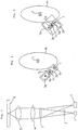
- the photodetector 17 has six photodetecting regions 17a - 17f, as shown in Fig. 8.
- the photodetecting regions 17a - 17d convert optical signals incident thereon to an information signal and a focus error signal, and the photodetecting regions 17e and 17f cooperate to produce a tracking error signal.
- a laser light beam emitted from the semiconductor laser device 11 is diffracted by the diffraction device 12 to be split into three separate beams: the main beam for producing an information signal and focus error signal in the three-beam method; and two sub-beams for producing a tracking error signal.
- the major portion of the beams propagates through the diffraction device 13, and then enters the object lens 15 via the collimating lens 14. Thereafter, these beams impinge on the recording medium 16, so that the main beam is focused on a pit of the recording medium 16 and the sub-beams are focused respectively on the positions in front of and behind the pit along the track direction.
- the main beam and sub-beams focused on the recording medium 16 are reflected therefrom. Then, the reflected main beam and sub-beams pass again the object lens 15 and collimating lens 14, and are diffracted by the diffraction device 13 so that the main beam is focused on the photodetecting regions 17a - 17d, and that the sub-beams are focused on the photodetecting regions 17e and 17f, respectively.
- the photodetecting regions 17e and 17f generate respectively outputs Se and Sf the level of each of which varies in accordance with the intensity of the sub-beam incident thereon.
- the tracking error signal can be obtained by calculating "Se - Sf".
- the sub-beam incident on the photodetecting region 17e is equal in intensity to that incident on the photodetecting region 17f so that the outputs Se and Sf are equal to each other, resulting in that the tracking error signal becomes zero.
- the sub-beam incident on the photodetecting region 17e is different in intensity from that incident on the photodetecting region 17f so that the outputs Se and Sf are different from each other, resulting in that the tracking error signal is not zero.
- the tracking error signal which is not zero causes the track servo control to be activated.
- the far field pattern of the laser light beam emitted from the semiconductor laser device 11 is an elliptical shape beam the center of which corresponds to the optical axis 11c, the minor axis of which is perpendicular to the optical axis 11c and parallel to the junction plane 11b of the laser device 11 and the major axis of which is perpendicular to the minor axis.
- the laser light beams incident on the recording medium 16 have an elliptical shape, but their spots formed on the recording medium 16 are changed in shape in accordance with the positional relationship between the laser device 11 and the photodetector 17.
- the spot of each laser light beam forms a long ellipse the major axis of which is perpendicular to the direction along the track (pit train), resulting in that the spot stretches to the adjacent tracks. This may cause the tracking error signal to be erroneously generated.
- the photodetector 17 is positioned so that the angle ⁇ is 90 deg.
- the spot of each laser light beam forms a long ellipse the major axis of which coincides with the direction along the track, resulting in inferior resolution while reading the length of the pit.
- the photodetector 17 is disposed at a position so that the angle ⁇ has a value other than 0, 90, 180 and 270 deg., thereby obtaining the information signal in an improved quality.
- the laser light beam emitted from the semiconductor laser device 11 is partly reflected by the diffraction devices 12 and 13, a member (not shown) for supporting the optical system, and holders (not shown) for mounting each optical elements, to become so-called stray light which does not contribute to the detection of signals such as the information signal.
- the stray light SL (Fig. 8) caused by the reflection at the diffraction devices 12 and 13 enters into the photodetector 17.
- the photodetector 17 receiving the stray light SL outputs signals based on the stray light.
- the optical intensity of the stray light SL distributes in an elliptical shape in the same manner as the laser light beam emitted from the laser device 11.
- the photodetector 17 is disposed at a position so that the angle ⁇ has a value other than 0, 90, 180 and 270 deg., therefore, the amount of the stray light SL received by the photodetecting region 17e is different from that received by the photodetecting region 17f, causing an offset in the tracking error signal.
- the photodetecting region 17f receives the stray light SL in a greater amount than the photodetecting region 17e, i.e., the output signal Sf of the photodetecting region 17f becomes greater than the output signal Se of the photodetecting region 17e (Se ⁇ Sf), so that the tracking error signal (Se - Sf) is not zero. This causes a problem in that the tracking control is erroneously conducted.
- An optical pickup apparatus in accordance with a first aspect of this invention, which aims to overcome the above-discussed and numerous other disadvantages and deficiencies of the prior art, comprises a laser light source for emitting a laser light beam, an optical lens system for converging the laser light onto a recording medium, a photodetector for detecting the laser light beam reflected from the recording medium, and a diffracting means disposed in the optical path extending between said laser light source and the recording medium, and is characterised by said diffracting means being provided with an antireflection means for preventing the laser light from being reflected.
- the antireflection means comprises an antireflection film formed on each of the two surfaces of said diffraction means.
- an optical pickup apparatus comprises a laser light source for emitting a laser light beam, an optical lens system for converging the laser light onto a recording medium, a photodetector for detecting the laser light beam reflected from the recording medium, and a diffracting means disposed in the optical path extending between said laser light source and the recording medium, said diffracting means dividing the laser light beam into three light beams for the three-beam method, and is characterised in that said photodetector comprises two photodetecting regions onto which two of said three light beams impinge respectively to produce a tracking error signal, the effective photodetecting areas of said photodetecting being different in size from each other.
- the distance between one of said two photodetecting regions and said laser light source is different from that between the other of said two photodetecting regions and said laser light source.
- the diffracting means is provided with an antireflection means for preventing the laser light from being reflected.
- an optical pickup apparatus comprises a laser light source for emitting a laser light beam; an optical lens sys the laser light onto a recording medium; a photodetector for detecting the laser light beam reflected from the recording medium; and a diffracting means disposed in the optical path extending between said laser light source and the recording medium, said diffracting means dividing the laser light beam into three light beams for the three-beam method, and is characterised in that said photodetector comprises two photodetecting regions onto which two of said three light beams impinge respectively to produce a tracking error signal, the distance between one of said two photodetecting regions and said laser light source being different from that between the other of said two photodetecting regions and said laser light source.
- the effective photodetecting areas of said photodetecting regions are different in size from each other
- the diffracting means is provided with an antireflection means for preventing the laser light from being reflected.
- the invention described herein makes possible the objectives of (1) providing an optical pickup apparatus which can generate a tracking error signal having no offset; (2) providing an optical pickup apparatus which can generate a correct tracking error signal; (3) providing an optical pickup apparatus the size of which can be reduced; and (4) providing an optical pickup apparatus the weight of which can be reduced.
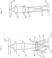
- Figure 1 shows an optical pickup apparatus according to the invention.
- the apparatus of Fig. 1 comprises a semiconductor laser device 1 for emitting a laser light beam, a diffraction device 3, a collimating lens 4, an object lens 5, and an photodetector 7.
- the photodetector 7 is disposed at the side of the semiconductor laser device 1.
- a laser beam emitted from the semiconductor is directed via the optical system to a recording medium 6 passes the diffraction device 3 and the collimating lens 4, and then focused on a recording medium 6 by the object lens 5.
- the light beam reflected from the recording medium 6 passes again the object lens 5 and the collimating lens 4, and then enters the diffraction device 3 to be diffracted.
- the diffraction beam from the diffraction device 3 enters the photodetector 7 which converts optical signals incident thereon to an information signal, a focus error signal and a tracking error signal.
- a diffraction grating is formed on the surface of the diffraction device 3 which faces the laser device 1.
- the diffraction device 3 is provided with an antireflection film 8a at the surface facing the recording medium 6, and also with an antireflection film 8b at the surface facing the laser device 1. Therefore, the laser light beam emitted from the laser device 1 is substantially prevented from being reflected by the diffraction device 3.
- only one of the surfaces of the diffraction device 3 may be provided with such an antireflection film.
- the manner of forming the antireflection film(s) is not restricted to the above.
- a very small portion of the laser light beam emitted from the semiconductor laser device 1 may be reflected by the diffraction device 3 while a major portion of the laser beam passes the diffraction device 3 as indicated by the arrows A1 (Fig. 1).
- the amount of the stray light is very small as compared with that of the light beam reflected from the recording medium and incident on the photodetector 7.
- the degree of the offset appearing in the output signals of the photodetector 7 is very small.
- Figure 3 shows another apparatus according to the invention.
- the apparatus of Fig. 3 is used for conducting the three-beam method, and is provided with a further diffraction device 2 between the semiconductor laser device 1 and the diffraction device 3.
- the laser light beam emitted from the laser device 1 is diffracted by the diffraction device 2 to be separated into a zero-order diffracted beam (main beam) and a pair of first-order diffracted beams (sub beams).
- the diffraction device 3 diffracts further the laser light beam to provide the laser beam reflected from the recording medium with the astigmatism, so that the laser light beam is directed to the photodetector 7.
- the photodetector 7 is disposed at the side of the laser device 1 and as shown in Fig.4, comprises six photodetecting regions 7a - 7f.
- the four photodetecting regions 7a - 7d are positioned at the center of the photodetector 7, and gathered to form a square. In other words, the four quarters of a square divided by the two diagonal lines constitute the regions 76 - 7d, respectively.
- the photodetecting regions 7e and 7f are positioned respectively at both end portions of the photodetector 7 to sandwich the assembly of the photodetecting regions 7a - 7d.
- the effective photodetecting areas of the regions 7e and 7f are different in size from each other so that the amount of the light beam incident on one of the regions 7e and 7f is equal to that of the light beam incident on the other of the regions 7e and 7f.
- the main beam and sub beams reflected from the recording medium 6 are diffracted by the diffraction device 3, and the first-order diffracted beams of the main beam and sub beams are directed to the photodetector 7, so that the main beam impinges on the point of intersection of the diagonal lines in the assembly of the photodetecting regions 7a - 7d and that the sub beams respectively impinge on the regions 7e and 7f.
- the photodetecting regions 7a - 7f produce optical outputs Sa - Sf, respectively.
- the focus signal is obtained by the calculation of " (Sa + Sc) - (Sb + Sd) ".
- the tracking error signal is detected in the three-beam method by calculating "Se - Sf".
- the information signal is obtained by calculating " Sa + Sb + Sc + Sd” .
- the effective photodetective area of each of the two photodetecting regions 7e and 7f can be freely set considering the amount of the stray light impinging thereon, the photodetector 7 can be disposed closer to the semiconductor laser device 1, resulting in the reduced size and weight of the optical pickup apparatus.
- Figure 5 illustrates the positional relation between the photodetector 7 and the semiconductor laser device 1 in a further optical pickup apparatus according to the invention.
- the construction of this embodiment is the same as that of the apparatus of Fig. 3 except that the the photodetector 7 is structured as shown in Fig. 5.
- the distance between the photodetecting region 7f and the laser device 1 is greater than that between the photodetecting region 7e and the laser device 1.
- the photodetector 7 can be disposed closer to the semiconductor laser device 1, resulting in the reduced size and weight of the optical pickup apparatus.
- the focus error is detected by the astigmatism method.
- the method for the focus error detection useful in the invention is not restricted to the astigmatism method, but can be selected from other methods known in the art. It will be easily understood for a skilled one in the art that the arrangements according to the invention which are described above can be combined in various ways.
Landscapes
- Physics & Mathematics (AREA)
- Optics & Photonics (AREA)
- Optical Head (AREA)
- Optical Recording Or Reproduction (AREA)
Applications Claiming Priority (7)
| Application Number | Priority Date | Filing Date | Title |
|---|---|---|---|
| JP63157253A JPH0675292B2 (ja) | 1988-06-23 | 1988-06-23 | 光ピックアップ装置 |
| JP15725588A JPH0675293B2 (ja) | 1988-06-23 | 1988-06-23 | 光ピックアップ装置 |
| JP63157254A JPH025235A (ja) | 1988-06-23 | 1988-06-23 | 光ピックアップ装置 |
| JP157255/88 | 1988-06-23 | ||
| JP157253/88 | 1988-06-23 | ||
| JP157254/88 | 1988-06-23 | ||
| EP89306387A EP0348221B1 (de) | 1988-06-23 | 1989-06-23 | Optische Abtastvorrichtung |
Related Parent Applications (2)
| Application Number | Title | Priority Date | Filing Date |
|---|---|---|---|
| EP89306387A Division EP0348221B1 (de) | 1988-06-23 | 1989-06-23 | Optische Abtastvorrichtung |
| EP89306387.5 Division | 1989-06-23 |
Publications (3)
| Publication Number | Publication Date |
|---|---|
| EP0612064A2 true EP0612064A2 (de) | 1994-08-24 |
| EP0612064A3 EP0612064A3 (de) | 1995-08-30 |
| EP0612064B1 EP0612064B1 (de) | 1997-10-29 |
Family
ID=27321133
Family Applications (2)
| Application Number | Title | Priority Date | Filing Date |
|---|---|---|---|
| EP94201533A Expired - Lifetime EP0612064B1 (de) | 1988-06-23 | 1989-06-23 | Optische Abtastvorrichtung |
| EP89306387A Expired - Lifetime EP0348221B1 (de) | 1988-06-23 | 1989-06-23 | Optische Abtastvorrichtung |
Family Applications After (1)
| Application Number | Title | Priority Date | Filing Date |
|---|---|---|---|
| EP89306387A Expired - Lifetime EP0348221B1 (de) | 1988-06-23 | 1989-06-23 | Optische Abtastvorrichtung |
Country Status (5)
| Country | Link |
|---|---|
| US (1) | US5408450A (de) |
| EP (2) | EP0612064B1 (de) |
| KR (1) | KR930005785B1 (de) |
| CA (1) | CA1324516C (de) |
| DE (2) | DE68928420T2 (de) |
Families Citing this family (12)
| Publication number | Priority date | Publication date | Assignee | Title |
|---|---|---|---|---|
| US5615200A (en) * | 1992-09-10 | 1997-03-25 | Kabushiki Kaisha Toshiba | Light beam shaping device to change an anisotropic beam to an isotropic beam for reducing the size of an optical head |
| US5517479A (en) * | 1993-03-26 | 1996-05-14 | Matsushita Electronics Corporation | Optical head including a semiconductor laser having a non-scatter incident area |
| JPH06302003A (ja) * | 1993-04-12 | 1994-10-28 | Rohm Co Ltd | 光ピックアップ |
| JP2000182253A (ja) * | 1998-12-15 | 2000-06-30 | Sony Corp | 情報記録再生装置 |
| US20020097660A1 (en) * | 2000-11-16 | 2002-07-25 | Matsushita Electric Industrial Co., Ltd. | Diffraction grating body, optical pick-up, semiconductor laser apparatus and optical information apparatus |
| US20030074098A1 (en) * | 2001-09-18 | 2003-04-17 | Cheung Robin W. | Integrated equipment set for forming an interconnect on a substrate |
| US20030220708A1 (en) * | 2001-11-28 | 2003-11-27 | Applied Materials, Inc. | Integrated equipment set for forming shallow trench isolation regions |
| JP4032732B2 (ja) * | 2001-12-20 | 2008-01-16 | ソニー株式会社 | 光ピックアップ装置 |
| US20040007325A1 (en) * | 2002-06-11 | 2004-01-15 | Applied Materials, Inc. | Integrated equipment set for forming a low K dielectric interconnect on a substrate |
| US20040206621A1 (en) * | 2002-06-11 | 2004-10-21 | Hongwen Li | Integrated equipment set for forming a low K dielectric interconnect on a substrate |
| US20050018297A1 (en) * | 2003-07-10 | 2005-01-27 | Konica Minolta Opto, Inc. | Optical component and optical pickup apparatus |
| CN108957465B (zh) * | 2018-06-07 | 2022-05-20 | 北京理工大学 | 一种多元异形光敏面接收的脉冲激光探测装置 |
Citations (10)
| Publication number | Priority date | Publication date | Assignee | Title |
|---|---|---|---|---|
| EP0223191A2 (de) * | 1985-11-20 | 1987-05-27 | Mitsubishi Denki Kabushiki Kaisha | Gerät mit optischem Kopf |
| EP0228620A2 (de) * | 1985-12-10 | 1987-07-15 | Nec Corporation | Optischer Kopf mit einem Beugungsgitter zum Richten von zwei oder mehreren gebeugten Lichtstrahlen auf optische Detektoren |
| JPS62209736A (ja) * | 1986-03-11 | 1987-09-14 | Mitsubishi Electric Corp | 光学式情報記録再生装置の光学ヘツド |
| JPS62209733A (ja) * | 1986-03-11 | 1987-09-14 | Mitsubishi Electric Corp | 光学式情報記録再生装置の光学ヘツド |
| EP0241372A1 (de) * | 1986-04-11 | 1987-10-14 | Thomson S.A. | Optische Leseeinrichtung für optische Aufnahmeträger |
| FR2601174A1 (fr) * | 1986-07-01 | 1988-01-08 | Mitsubishi Electric Corp | Dispositif formant tete de type optique, notamment pour l'enregistrement et la lecture de donnees. |
| EP0268357A2 (de) * | 1986-09-20 | 1988-05-25 | Fujitsu Limited | Optisches System aus Hologrammlinsen |
| JPS63148429A (ja) * | 1986-12-12 | 1988-06-21 | Nec Corp | 光ヘツド装置 |
| EP0305169A2 (de) * | 1987-08-24 | 1989-03-01 | Sharp Kabushiki Kaisha | Optische Abtastvorrichtung und optische Gitteranordnung dazu |
| EP0309689A2 (de) * | 1987-09-28 | 1989-04-05 | Nec Home Electronics, Ltd. | Optische Abtastvorrichtung und holographischer Strahlteiler dafür |
Family Cites Families (14)
| Publication number | Priority date | Publication date | Assignee | Title |
|---|---|---|---|---|
| FR2266932B1 (de) * | 1973-03-02 | 1977-09-02 | Thomson Brandt | |
| US4314262A (en) * | 1980-02-04 | 1982-02-02 | Xerox Corporation | Optical data recording medium |
| JPS59231736A (ja) * | 1983-06-13 | 1984-12-26 | Hitachi Ltd | フォーカスおよびトラッキング誤差検出装置 |
| JPS6028035A (ja) * | 1983-07-26 | 1985-02-13 | Nippon Kogaku Kk <Nikon> | 光学式情報再生装置のフオ−カス誤差検出装置 |
| CA1257392A (en) * | 1985-03-20 | 1989-07-11 | Masayuki Kato | Optical pickup with hologram lenses |
| JPH07105055B2 (ja) * | 1985-11-20 | 1995-11-13 | 三菱電機株式会社 | 光学ヘツド装置 |
| EP0225564A3 (en) * | 1985-11-30 | 1988-07-06 | Kabushiki Kaisha Toshiba | Optical head |
| NL8601974A (nl) * | 1986-08-01 | 1988-03-01 | Philips Nv | Inrichting voor het met optische straling aftasten van een stralingsreflekterend informatievlak. |
| US4789977A (en) * | 1986-11-06 | 1988-12-06 | Laser Magnetic Storage International Company | Optical data recording device |
| NL8702245A (nl) * | 1987-09-21 | 1989-04-17 | Philips Nv | Inrichting voor het met optische straling aftasten van een stralingsreflekterend informatievlak. |
| JP2639659B2 (ja) * | 1987-11-02 | 1997-08-13 | セイコーエプソン株式会社 | 光ヘッド |
| US4823220A (en) * | 1987-11-16 | 1989-04-18 | International Business Machines Corporation | Detector for magnetooptic recorders |
| JPH01151022A (ja) * | 1987-12-09 | 1989-06-13 | Sharp Corp | 光ピックアップ装置 |
| NL8800057A (nl) * | 1988-01-11 | 1989-08-01 | Philips Nv | Optische aftastinrichting. |
-
1989
- 1989-06-23 KR KR1019890008718A patent/KR930005785B1/ko not_active IP Right Cessation
- 1989-06-23 EP EP94201533A patent/EP0612064B1/de not_active Expired - Lifetime
- 1989-06-23 CA CA000603765A patent/CA1324516C/en not_active Expired - Lifetime
- 1989-06-23 DE DE68928420T patent/DE68928420T2/de not_active Expired - Lifetime
- 1989-06-23 EP EP89306387A patent/EP0348221B1/de not_active Expired - Lifetime
- 1989-06-23 DE DE68919922T patent/DE68919922T2/de not_active Expired - Lifetime
-
1993
- 1993-04-28 US US08/053,334 patent/US5408450A/en not_active Expired - Lifetime
Patent Citations (10)
| Publication number | Priority date | Publication date | Assignee | Title |
|---|---|---|---|---|
| EP0223191A2 (de) * | 1985-11-20 | 1987-05-27 | Mitsubishi Denki Kabushiki Kaisha | Gerät mit optischem Kopf |
| EP0228620A2 (de) * | 1985-12-10 | 1987-07-15 | Nec Corporation | Optischer Kopf mit einem Beugungsgitter zum Richten von zwei oder mehreren gebeugten Lichtstrahlen auf optische Detektoren |
| JPS62209736A (ja) * | 1986-03-11 | 1987-09-14 | Mitsubishi Electric Corp | 光学式情報記録再生装置の光学ヘツド |
| JPS62209733A (ja) * | 1986-03-11 | 1987-09-14 | Mitsubishi Electric Corp | 光学式情報記録再生装置の光学ヘツド |
| EP0241372A1 (de) * | 1986-04-11 | 1987-10-14 | Thomson S.A. | Optische Leseeinrichtung für optische Aufnahmeträger |
| FR2601174A1 (fr) * | 1986-07-01 | 1988-01-08 | Mitsubishi Electric Corp | Dispositif formant tete de type optique, notamment pour l'enregistrement et la lecture de donnees. |
| EP0268357A2 (de) * | 1986-09-20 | 1988-05-25 | Fujitsu Limited | Optisches System aus Hologrammlinsen |
| JPS63148429A (ja) * | 1986-12-12 | 1988-06-21 | Nec Corp | 光ヘツド装置 |
| EP0305169A2 (de) * | 1987-08-24 | 1989-03-01 | Sharp Kabushiki Kaisha | Optische Abtastvorrichtung und optische Gitteranordnung dazu |
| EP0309689A2 (de) * | 1987-09-28 | 1989-04-05 | Nec Home Electronics, Ltd. | Optische Abtastvorrichtung und holographischer Strahlteiler dafür |
Non-Patent Citations (3)
| Title |
|---|
| PATENT ABSTRACTS OF JAPAN vol. 012 no. 071 (P-673) ,5 March 1988 & JP-A-62 209733 (MITSUBISHI ELECTRIC CORP) 14 September 1987, * |
| PATENT ABSTRACTS OF JAPAN vol. 012 no. 071 (P-673) ,5 March 1988 & JP-A-62 209736 (MITSUBISHI ELECTRIC CORP) 14 September 1987, * |
| PATENT ABSTRACTS OF JAPAN vol. 012 no. 411 (P-779) ,31 October 1988 & JP-A-63 148429 (NEC CORP) 21 June 1988, * |
Also Published As
| Publication number | Publication date |
|---|---|
| US5408450A (en) | 1995-04-18 |
| DE68919922D1 (de) | 1995-01-26 |
| KR930005785B1 (ko) | 1993-06-24 |
| EP0348221A2 (de) | 1989-12-27 |
| DE68919922T2 (de) | 1995-06-22 |
| EP0348221A3 (de) | 1991-05-15 |
| CA1324516C (en) | 1993-11-23 |
| EP0612064B1 (de) | 1997-10-29 |
| EP0612064A3 (de) | 1995-08-30 |
| DE68928420D1 (de) | 1997-12-04 |
| KR910001670A (ko) | 1991-01-31 |
| EP0348221B1 (de) | 1994-12-14 |
| DE68928420T2 (de) | 1998-04-16 |
Similar Documents
| Publication | Publication Date | Title |
|---|---|---|
| EP0357323B1 (de) | Optische Abtastvorrichtung | |
| US5016954A (en) | Optical pickup and hologram therefor | |
| US5111449A (en) | Optical pick-up device using diffraction grating element having two sub-regions | |
| KR880001707B1 (ko) | 광전자 집속에러 검출장치 | |
| USRE35332E (en) | Optical pickup device with diffraction device | |
| JPS6297141A (ja) | 光学走査装置 | |
| US5608695A (en) | Optical pick-up apparatus with tracking error detection by detection of amount of light in fan field | |
| EP0554092B1 (de) | Gerät zur Aufzeichnung und Wiedergabe von optischen Informationen | |
| US4771411A (en) | Device for scanning a radiation-reflecting information surface with optical radiation | |
| JPS5856236A (ja) | 光学的トラック位置検出装置およびそれを用いた光学的記録再生装置 | |
| EP0348221B1 (de) | Optische Abtastvorrichtung | |
| US5231621A (en) | Focus detector which serves to split off a portion of a detected light beam only when the detected light beam is not refocused at an expected refocus point | |
| US5500846A (en) | Radiation source-detection unit employing a grating having two grating structures, and a device including that unit | |
| US5570334A (en) | Optical pickup with a double refraction polarizing plate to split light beams into two polarized beams | |
| US4633454A (en) | Optical information pickup apparatus | |
| US5144131A (en) | Device for optically scanning an information plane detecting border portions of light beam | |
| EP0273422A2 (de) | Verfahren und Gerät zur Erfassung von Ausrichtungs- und Fokusfehlern in einem optischen Kopf | |
| US6512732B1 (en) | Device for optically scanning information tracks on a plane using two subbeams | |
| JPH06274904A (ja) | 光ピックアップ装置 | |
| EP0605929B1 (de) | Vorrichtung zur optischen Abtastung einer Fläche | |
| US7016274B2 (en) | Optical pickup system with light receiving portion | |
| JPS6331858B2 (de) | ||
| EP1067532B1 (de) | Optische Abtasteinheit und optisches Plattengerät | |
| JP2788723B2 (ja) | 光スポツト位置エラー検出装置 | |
| KR200172921Y1 (ko) | 홀로그램소자를 채용한 광픽업 장치 |
Legal Events
| Date | Code | Title | Description |
|---|---|---|---|
| PUAI | Public reference made under article 153(3) epc to a published international application that has entered the european phase |
Free format text: ORIGINAL CODE: 0009012 |
|
| 17P | Request for examination filed |
Effective date: 19940531 |
|
| AC | Divisional application: reference to earlier application |
Ref document number: 348221 Country of ref document: EP |
|
| AK | Designated contracting states |
Kind code of ref document: A2 Designated state(s): DE FR GB NL |
|
| RIN1 | Information on inventor provided before grant (corrected) |
Inventor name: KURATA, YUKIO Inventor name: NAGAHAMA, TOSHIYA |
|
| PUAL | Search report despatched |
Free format text: ORIGINAL CODE: 0009013 |
|
| AK | Designated contracting states |
Kind code of ref document: A3 Designated state(s): DE FR GB NL |
|
| RIN1 | Information on inventor provided before grant (corrected) |
Inventor name: YOSHIDA, YOSHIO Inventor name: KURATA, YUKIO Inventor name: NAGAHAMA, TOSHIYA |
|
| 17Q | First examination report despatched |
Effective date: 19960729 |
|
| GRAG | Despatch of communication of intention to grant |
Free format text: ORIGINAL CODE: EPIDOS AGRA |
|
| GRAH | Despatch of communication of intention to grant a patent |
Free format text: ORIGINAL CODE: EPIDOS IGRA |
|
| GRAH | Despatch of communication of intention to grant a patent |
Free format text: ORIGINAL CODE: EPIDOS IGRA |
|
| GRAA | (expected) grant |
Free format text: ORIGINAL CODE: 0009210 |
|
| AC | Divisional application: reference to earlier application |
Ref document number: 348221 Country of ref document: EP |
|
| AK | Designated contracting states |
Kind code of ref document: B1 Designated state(s): DE FR GB NL |
|
| RIN1 | Information on inventor provided before grant (corrected) |
Inventor name: YOSHIDA, YOSHIO Inventor name: KURATA, YUKIO Inventor name: NAGAHAMA, TOSHIYA |
|
| REF | Corresponds to: |
Ref document number: 68928420 Country of ref document: DE Date of ref document: 19971204 |
|
| ET | Fr: translation filed | ||
| PLBE | No opposition filed within time limit |
Free format text: ORIGINAL CODE: 0009261 |
|
| STAA | Information on the status of an ep patent application or granted ep patent |
Free format text: STATUS: NO OPPOSITION FILED WITHIN TIME LIMIT |
|
| 26N | No opposition filed | ||
| REG | Reference to a national code |
Ref country code: GB Ref legal event code: IF02 |
|
| PGFP | Annual fee paid to national office [announced via postgrant information from national office to epo] |
Ref country code: NL Payment date: 20080603 Year of fee payment: 20 Ref country code: DE Payment date: 20080626 Year of fee payment: 20 |
|
| PGFP | Annual fee paid to national office [announced via postgrant information from national office to epo] |
Ref country code: FR Payment date: 20080617 Year of fee payment: 20 |
|
| PGFP | Annual fee paid to national office [announced via postgrant information from national office to epo] |
Ref country code: GB Payment date: 20080625 Year of fee payment: 20 |
|
| REG | Reference to a national code |
Ref country code: GB Ref legal event code: PE20 Expiry date: 20090622 |
|
| PG25 | Lapsed in a contracting state [announced via postgrant information from national office to epo] |
Ref country code: NL Free format text: LAPSE BECAUSE OF EXPIRATION OF PROTECTION Effective date: 20090623 |
|
| NLV7 | Nl: ceased due to reaching the maximum lifetime of a patent |
Effective date: 20090623 |
|
| PG25 | Lapsed in a contracting state [announced via postgrant information from national office to epo] |
Ref country code: GB Free format text: LAPSE BECAUSE OF EXPIRATION OF PROTECTION Effective date: 20090622 |