EP0608458B1 - Verfahren zur Steuerung einer optischen Modulationsvorrichtung - Google Patents
Verfahren zur Steuerung einer optischen Modulationsvorrichtung Download PDFInfo
- Publication number
- EP0608458B1 EP0608458B1 EP93101362A EP93101362A EP0608458B1 EP 0608458 B1 EP0608458 B1 EP 0608458B1 EP 93101362 A EP93101362 A EP 93101362A EP 93101362 A EP93101362 A EP 93101362A EP 0608458 B1 EP0608458 B1 EP 0608458B1
- Authority
- EP
- European Patent Office
- Prior art keywords
- liquid crystal
- electrodes
- electrode
- pixel
- crystal layer
- Prior art date
- Legal status (The legal status is an assumption and is not a legal conclusion. Google has not performed a legal analysis and makes no representation as to the accuracy of the status listed.)
- Expired - Lifetime
Links
Images


Classifications
-
- G—PHYSICS
- G02—OPTICS
- G02F—OPTICAL DEVICES OR ARRANGEMENTS FOR THE CONTROL OF LIGHT BY MODIFICATION OF THE OPTICAL PROPERTIES OF THE MEDIA OF THE ELEMENTS INVOLVED THEREIN; NON-LINEAR OPTICS; FREQUENCY-CHANGING OF LIGHT; OPTICAL LOGIC ELEMENTS; OPTICAL ANALOGUE/DIGITAL CONVERTERS
- G02F1/00—Devices or arrangements for the control of the intensity, colour, phase, polarisation or direction of light arriving from an independent light source, e.g. switching, gating or modulating; Non-linear optics
- G02F1/01—Devices or arrangements for the control of the intensity, colour, phase, polarisation or direction of light arriving from an independent light source, e.g. switching, gating or modulating; Non-linear optics for the control of the intensity, phase, polarisation or colour
- G02F1/13—Devices or arrangements for the control of the intensity, colour, phase, polarisation or direction of light arriving from an independent light source, e.g. switching, gating or modulating; Non-linear optics for the control of the intensity, phase, polarisation or colour based on liquid crystals, e.g. single liquid crystal display cells
- G02F1/133—Constructional arrangements; Operation of liquid crystal cells; Circuit arrangements
- G02F1/136—Liquid crystal cells structurally associated with a semi-conducting layer or substrate, e.g. cells forming part of an integrated circuit
- G02F1/1362—Active matrix addressed cells
- G02F1/1365—Active matrix addressed cells in which the switching element is a two-electrode device
-
- G—PHYSICS
- G02—OPTICS
- G02F—OPTICAL DEVICES OR ARRANGEMENTS FOR THE CONTROL OF LIGHT BY MODIFICATION OF THE OPTICAL PROPERTIES OF THE MEDIA OF THE ELEMENTS INVOLVED THEREIN; NON-LINEAR OPTICS; FREQUENCY-CHANGING OF LIGHT; OPTICAL LOGIC ELEMENTS; OPTICAL ANALOGUE/DIGITAL CONVERTERS
- G02F1/00—Devices or arrangements for the control of the intensity, colour, phase, polarisation or direction of light arriving from an independent light source, e.g. switching, gating or modulating; Non-linear optics
- G02F1/01—Devices or arrangements for the control of the intensity, colour, phase, polarisation or direction of light arriving from an independent light source, e.g. switching, gating or modulating; Non-linear optics for the control of the intensity, phase, polarisation or colour
- G02F1/13—Devices or arrangements for the control of the intensity, colour, phase, polarisation or direction of light arriving from an independent light source, e.g. switching, gating or modulating; Non-linear optics for the control of the intensity, phase, polarisation or colour based on liquid crystals, e.g. single liquid crystal display cells
- G02F1/133—Constructional arrangements; Operation of liquid crystal cells; Circuit arrangements
- G02F1/1333—Constructional arrangements; Manufacturing methods
- G02F1/1343—Electrodes
- G02F1/134309—Electrodes characterised by their geometrical arrangement
- G02F1/134336—Matrix
-
- G—PHYSICS
- G02—OPTICS
- G02F—OPTICAL DEVICES OR ARRANGEMENTS FOR THE CONTROL OF LIGHT BY MODIFICATION OF THE OPTICAL PROPERTIES OF THE MEDIA OF THE ELEMENTS INVOLVED THEREIN; NON-LINEAR OPTICS; FREQUENCY-CHANGING OF LIGHT; OPTICAL LOGIC ELEMENTS; OPTICAL ANALOGUE/DIGITAL CONVERTERS
- G02F1/00—Devices or arrangements for the control of the intensity, colour, phase, polarisation or direction of light arriving from an independent light source, e.g. switching, gating or modulating; Non-linear optics
- G02F1/29—Devices or arrangements for the control of the intensity, colour, phase, polarisation or direction of light arriving from an independent light source, e.g. switching, gating or modulating; Non-linear optics for the control of the position or the direction of light beams, i.e. deflection
- G02F1/292—Devices or arrangements for the control of the intensity, colour, phase, polarisation or direction of light arriving from an independent light source, e.g. switching, gating or modulating; Non-linear optics for the control of the position or the direction of light beams, i.e. deflection by controlled diffraction or phased-array beam steering
-
- G—PHYSICS
- G02—OPTICS
- G02F—OPTICAL DEVICES OR ARRANGEMENTS FOR THE CONTROL OF LIGHT BY MODIFICATION OF THE OPTICAL PROPERTIES OF THE MEDIA OF THE ELEMENTS INVOLVED THEREIN; NON-LINEAR OPTICS; FREQUENCY-CHANGING OF LIGHT; OPTICAL LOGIC ELEMENTS; OPTICAL ANALOGUE/DIGITAL CONVERTERS
- G02F1/00—Devices or arrangements for the control of the intensity, colour, phase, polarisation or direction of light arriving from an independent light source, e.g. switching, gating or modulating; Non-linear optics
- G02F1/01—Devices or arrangements for the control of the intensity, colour, phase, polarisation or direction of light arriving from an independent light source, e.g. switching, gating or modulating; Non-linear optics for the control of the intensity, phase, polarisation or colour
- G02F1/13—Devices or arrangements for the control of the intensity, colour, phase, polarisation or direction of light arriving from an independent light source, e.g. switching, gating or modulating; Non-linear optics for the control of the intensity, phase, polarisation or colour based on liquid crystals, e.g. single liquid crystal display cells
- G02F1/133—Constructional arrangements; Operation of liquid crystal cells; Circuit arrangements
- G02F1/1333—Constructional arrangements; Manufacturing methods
- G02F1/1347—Arrangement of liquid crystal layers or cells in which the final condition of one light beam is achieved by the addition of the effects of two or more layers or cells
-
- G—PHYSICS
- G02—OPTICS
- G02F—OPTICAL DEVICES OR ARRANGEMENTS FOR THE CONTROL OF LIGHT BY MODIFICATION OF THE OPTICAL PROPERTIES OF THE MEDIA OF THE ELEMENTS INVOLVED THEREIN; NON-LINEAR OPTICS; FREQUENCY-CHANGING OF LIGHT; OPTICAL LOGIC ELEMENTS; OPTICAL ANALOGUE/DIGITAL CONVERTERS
- G02F1/00—Devices or arrangements for the control of the intensity, colour, phase, polarisation or direction of light arriving from an independent light source, e.g. switching, gating or modulating; Non-linear optics
- G02F1/01—Devices or arrangements for the control of the intensity, colour, phase, polarisation or direction of light arriving from an independent light source, e.g. switching, gating or modulating; Non-linear optics for the control of the intensity, phase, polarisation or colour
- G02F1/13—Devices or arrangements for the control of the intensity, colour, phase, polarisation or direction of light arriving from an independent light source, e.g. switching, gating or modulating; Non-linear optics for the control of the intensity, phase, polarisation or colour based on liquid crystals, e.g. single liquid crystal display cells
- G02F1/137—Devices or arrangements for the control of the intensity, colour, phase, polarisation or direction of light arriving from an independent light source, e.g. switching, gating or modulating; Non-linear optics for the control of the intensity, phase, polarisation or colour based on liquid crystals, e.g. single liquid crystal display cells characterised by the electro-optical or magneto-optical effect, e.g. field-induced phase transition, orientation effect, guest-host interaction or dynamic scattering
- G02F1/139—Devices or arrangements for the control of the intensity, colour, phase, polarisation or direction of light arriving from an independent light source, e.g. switching, gating or modulating; Non-linear optics for the control of the intensity, phase, polarisation or colour based on liquid crystals, e.g. single liquid crystal display cells characterised by the electro-optical or magneto-optical effect, e.g. field-induced phase transition, orientation effect, guest-host interaction or dynamic scattering based on orientation effects in which the liquid crystal remains transparent
- G02F1/1396—Devices or arrangements for the control of the intensity, colour, phase, polarisation or direction of light arriving from an independent light source, e.g. switching, gating or modulating; Non-linear optics for the control of the intensity, phase, polarisation or colour based on liquid crystals, e.g. single liquid crystal display cells characterised by the electro-optical or magneto-optical effect, e.g. field-induced phase transition, orientation effect, guest-host interaction or dynamic scattering based on orientation effects in which the liquid crystal remains transparent the liquid crystal being selectively controlled between a twisted state and a non-twisted state, e.g. TN-LC cell
- G02F1/1397—Devices or arrangements for the control of the intensity, colour, phase, polarisation or direction of light arriving from an independent light source, e.g. switching, gating or modulating; Non-linear optics for the control of the intensity, phase, polarisation or colour based on liquid crystals, e.g. single liquid crystal display cells characterised by the electro-optical or magneto-optical effect, e.g. field-induced phase transition, orientation effect, guest-host interaction or dynamic scattering based on orientation effects in which the liquid crystal remains transparent the liquid crystal being selectively controlled between a twisted state and a non-twisted state, e.g. TN-LC cell the twist being substantially higher than 90°, e.g. STN-, SBE-, OMI-LC cells
-
- G—PHYSICS
- G02—OPTICS
- G02F—OPTICAL DEVICES OR ARRANGEMENTS FOR THE CONTROL OF LIGHT BY MODIFICATION OF THE OPTICAL PROPERTIES OF THE MEDIA OF THE ELEMENTS INVOLVED THEREIN; NON-LINEAR OPTICS; FREQUENCY-CHANGING OF LIGHT; OPTICAL LOGIC ELEMENTS; OPTICAL ANALOGUE/DIGITAL CONVERTERS
- G02F1/00—Devices or arrangements for the control of the intensity, colour, phase, polarisation or direction of light arriving from an independent light source, e.g. switching, gating or modulating; Non-linear optics
- G02F1/01—Devices or arrangements for the control of the intensity, colour, phase, polarisation or direction of light arriving from an independent light source, e.g. switching, gating or modulating; Non-linear optics for the control of the intensity, phase, polarisation or colour
- G02F1/13—Devices or arrangements for the control of the intensity, colour, phase, polarisation or direction of light arriving from an independent light source, e.g. switching, gating or modulating; Non-linear optics for the control of the intensity, phase, polarisation or colour based on liquid crystals, e.g. single liquid crystal display cells
- G02F1/137—Devices or arrangements for the control of the intensity, colour, phase, polarisation or direction of light arriving from an independent light source, e.g. switching, gating or modulating; Non-linear optics for the control of the intensity, phase, polarisation or colour based on liquid crystals, e.g. single liquid crystal display cells characterised by the electro-optical or magneto-optical effect, e.g. field-induced phase transition, orientation effect, guest-host interaction or dynamic scattering
- G02F1/139—Devices or arrangements for the control of the intensity, colour, phase, polarisation or direction of light arriving from an independent light source, e.g. switching, gating or modulating; Non-linear optics for the control of the intensity, phase, polarisation or colour based on liquid crystals, e.g. single liquid crystal display cells characterised by the electro-optical or magneto-optical effect, e.g. field-induced phase transition, orientation effect, guest-host interaction or dynamic scattering based on orientation effects in which the liquid crystal remains transparent
- G02F1/141—Devices or arrangements for the control of the intensity, colour, phase, polarisation or direction of light arriving from an independent light source, e.g. switching, gating or modulating; Non-linear optics for the control of the intensity, phase, polarisation or colour based on liquid crystals, e.g. single liquid crystal display cells characterised by the electro-optical or magneto-optical effect, e.g. field-induced phase transition, orientation effect, guest-host interaction or dynamic scattering based on orientation effects in which the liquid crystal remains transparent using ferroelectric liquid crystals
- G02F1/1412—Antiferroelectric liquid crystals
-
- G—PHYSICS
- G02—OPTICS
- G02F—OPTICAL DEVICES OR ARRANGEMENTS FOR THE CONTROL OF LIGHT BY MODIFICATION OF THE OPTICAL PROPERTIES OF THE MEDIA OF THE ELEMENTS INVOLVED THEREIN; NON-LINEAR OPTICS; FREQUENCY-CHANGING OF LIGHT; OPTICAL LOGIC ELEMENTS; OPTICAL ANALOGUE/DIGITAL CONVERTERS
- G02F2203/00—Function characteristic
- G02F2203/12—Function characteristic spatial light modulator
-
- G—PHYSICS
- G02—OPTICS
- G02F—OPTICAL DEVICES OR ARRANGEMENTS FOR THE CONTROL OF LIGHT BY MODIFICATION OF THE OPTICAL PROPERTIES OF THE MEDIA OF THE ELEMENTS INVOLVED THEREIN; NON-LINEAR OPTICS; FREQUENCY-CHANGING OF LIGHT; OPTICAL LOGIC ELEMENTS; OPTICAL ANALOGUE/DIGITAL CONVERTERS
- G02F2203/00—Function characteristic
- G02F2203/22—Function characteristic diffractive
Definitions
- This invention relates to a method of operating a spatial optical modulator device for effecting modulation of an optical wave surface.
- the present invention relates to a method of driving a fine electrode liquid crystal device type spatial optical modulator device in order to generate a diffractive pattern.
- a diffraction plate using a photographic method a diffraction grating using mechanical machining or an optical lens has been widely used in the past, while an acoustico-optical device and a transparent piezoelectric device such as a PLZT have been used to effect control that changes with time.
- a precision stationary optical wave surface modulation device fabricated in the course of time can be utilized for time-fixed control of the optical wave surface, but a pattern updating time of the optical wave surface modulation device must be as fast as up to about tens of milli-seconds for moving pictures. It is possible to mechanically switch a large number of holograms that have been taken in advance and reproduce them as moving pictures, as in motion pictures.
- a phase modulator device of an optical wave surface for forming a pattern by an electron beam on an oil film and controlling the film thickness requires large scale vacuum tubes and exhaust systems, and the life of the oil film is short so this method is not easy to apply.
- a system that scans a smectic liquid crystal using a laser beam has a resolution of up to micrometers, but since a thermal write system is employed, a long time is necessary for heat transfer and heat equilibrium. In other words, about one second is necessary for drawing one screen, and this drawing speed is not sufficient.
- Liquid crystal video display devices that have been developed for the display of liquid crystal television receivers and personal computers have a low response speed of 20 msec to 50 msec because they are designed to correspond to moving pictures. From the viewpoint of response speed and pixel density, liquid crystal devices for display are effective devices, and the feasibility of using the liquid crystal display device as a diffraction grating has been examined in the past. However, according to an estimation of the practical size limits of the liquid crystal pixels, the lower limit is regarded as being some tens of microns.
- the minimum dimension of each of the widths of the pixel electrode and the gap between the pixel electrodes is 5 ⁇ m, that is, the pixel pitch is about 10 ⁇ m and even in the case of ferroelectric liquid crystal devices, the limit is about 4 ⁇ m, and the resolution is 100 to 250 (lines/mm). A higher resolution has been believed impossible in view of the limit of the thickness of the liquid crystal layer.
- the present invention provides a method of correctly realizing shape accuracy and positional accuracy of a diffraction pattern to be formed, by precisely controlling a group of liquid crystal molecules as a function of a location near a fine synthetic electric field which is generated by combining pixels, which are smaller than the thickness of a liquid crystal layer, and gaps between the pixels.
- the present invention discloses a method of producing diffraction pattern using liquid crystal cell structure, orientation and material necessary for realizing this device structure, and application examples effectively utilizing the features of the diffraction device according to the present invention.
- the size of a pixel of a liquid crystal display device used for personal computers and word processors has been determined on the premise that one pixel can be visually identified as one dot by most people. Therefore, the dimensions of a pixel in the liquid crystal device has been established to be 250 to 350 ⁇ m, and the gap between the pixels is about 10% of the pixel dimension, that is, from 25 to 35 ⁇ m, in order to obtain an aperture ratio of at least 80% and to improve a production yield.
- the pixels themselves need not be discriminated, but the screen becomes easier to view if the pixels are not distinctive. For this reason, devices having a pixel dimension of 100 to 200 ⁇ m have been used.
- the width of the pixel electrode and the electrode gap are set to 18 ⁇ m and 6 ⁇ m, respectively, to secure an aperture ratio of at least 50% when the thickness of the liquid crystal layer is 5 ⁇ m, resolution is about 40 lines/mm, and this value is by far lower than the level necessary for holography, that is, from hundreds to thousands of lines per millimeter.
- the electrode pitch is reduced, the aperture ratio of the pixel drastically decreases, and resolution of at least some tens of lines per millimeter is believed unrealistic. Accordingly, the pursuit of higher resulution has been abandoned.
- US Patent 5,136,407 discloses a liquid crystal device suitable for use as a focusing screen within a video camera and the like.
- the device comprises a pair of transparent insulating substrates having opposed surfaces and two groups of opposed electrodes disposed in a parallel and evenly spaced pattern on a respective one of said substrate surfaces.
- a liquid crystal layer is sandwiched between said opposite substrate surfaces.
- the electrodes may have a width smaller than the thickness of the liquid crystal layer, and said electrode width may be less than the gap distance between electrodes disposed adjacent to one another. According to the presence or absence of corresponding voltages applied to the electrodes, the focusing screen changes between a transparent state and a scattered state. Two different voltages are applied to alternate electrodes of a respective electrode group.
- the gap distance between the electrodes of one group is in the order of 50 ⁇ m, while in another embodiment the gap distance and the electrode width are chosen equal to 5 ⁇ m. In another embodiment the electrode width is 3 ⁇ m, the gap is 17 ⁇ m, and the liquid crystal layer thickness is 30 ⁇ m.
- the electrode structure consists of a comb-like grating structure on either side of the liquid crystal layer extending almost perpendicular to one another. Two voltages of rectangular wave form of 1kHz and of peak-to-peak values of 10V and 0V are applied to each of a pair of successive grating parts of each of the two opposing electrode comb structures.
- the problem to be solved by the present invention resides in the accomplishment of a diffraction pattern formation of an optical wave surface modulator device for electronic control on a real-time basis by the use of a liquid crystal diffraction device driving method with a higher level of accuracy. More specifically, the present invention is directed to the following points:
- the present invention not only reduces the thickness of the liquid crystal layer, but also effects control of a fine electric field distribution for the formation of a fine diffraction pattern.
- the present invention clarifies an electrode structure as well as a driving method for these purposes.
- the dimension of a pixel electrode is recognized as being equal to the pixel dimension, and the gap between the adjacent electrodes in a transverse direction has been handled as an unnecessary region which is not electrically controlled, or as a frame region for lowering an aperture ratio of the pixel. From these points of view, the decrease of the electrode dimension invites lowering of the aperture ratio, and this provides the lower limit of the pixel pitch.
- the "electrode gap dimension" described above is approximately 20 ⁇ m in the case of a large personal computer and is 5 to 15 ⁇ m in the case of a liquid crystal device for a small television receiver.
- the lower limit dimension of the pitch when the liquid crystal device is designed as a spatial modulator device in addition to the display device is the sum of the pixel gap, which is substantially equal to the thickness of the liquid crystal layer, and the electrode dimension of about the same size, that is, at least 10 ⁇ m pitch.
- the aperture ratio in this case is believed to be not greater than 25%. For these reasons, a further miniaturized liquid crystal device of not greater than 10 ⁇ m has been believed unrealistic due to the drop in the aperture ratio.
- Positional accuracy of a reproduced image depends on positional accuracy of the hologram, and when precise positioning of the reproduced image is necessary, positional accuracy of the diffraction pattern itself of the hologram becomes necessary.
- the spatial frequency of the diffraction pattern of the hologram decreases as a sinusoidal function of an intersection angle between a reference beam and an object beam. Accordingly, the pitch of the diffraction pattern can be increased by reducing this intersection angle.
- this pitch dimension and accuracy of the position and dimension of the diffraction pattern are essentially independent of one another, and there is a case where a permissible positional error of the diffraction pattern is by far smaller than a half wavelength distance of the spatial frequency of the diffraction pattern, depending on the situation.
- a permissible positional error of the diffraction pattern is by far smaller than a half wavelength distance of the spatial frequency of the diffraction pattern, depending on the situation.
- a hologram is formed and an image is reproduced by the use of a liquid crystal device. From the aspect of the formation of the image, an image formation becomes easier by reducing the intersection angle of the object beam and the reference beam to make the pitch of the diffraction pattern coarser. Fine pixels are necessary to accurately reproduce the position of a reproduced pattern.
- the electrode gap is left constant, the aperture ratio drops even in the case of the electrodes having a smaller dimension than the thickness of the liquid crystal layer, and beam utilization efficiency drops markedly.
- the electrodes themselves for forming the diffraction pattern must be smaller than the pitch of the diffraction pattern, and the pattern must be reproduced accurately.
- the first contrivance is the control of the liquid crystal layer immediately below the gap of the electrodes. Conventionally, this region is the region of which the control by the electrodes has been discarded. Therefore, means for allowing driving of this gap is first considered.
- the dimension of the driving electrode is reduced, a ratio of swelling of lines of electric force at peripheral portions increases. This effect becomes all the more effective when the electrode dimension is small in comparison with the thickness of the liquid crystal layer.
- the dimension of the electrode gap is kept at a minimum necessary constant value, the proportion of the electrode dimension can be reduced to a dimension below a similar ratio, and the occupying ratio of the gap in this case is the square of the dimensional ratio and becomes greater than the electrode area.
- the dimension of the electrode pitch for forming the pixel can be reduced to minimum.
- the influence of the electric field generated by the electrodes under the driving condition of the liquid crystal molecule group by this fine pixel electrode group on the surrounding area can be considered in accordance with the principle of superposition, and the electric field distribution immediately below the gap between the electrodes can be controlled by the vector sum of the electric fields formed for a large number of individual surrounding electrodes.
- this pixel to be turned ON is buried in the OFF electric field as it is pulled by the surrounding OFF electric field, and is not turned ON.
- the ON electrode group region can be lit because the electric fields are superposed with one another.
- the pattern formation position as well as the pattern formation can be set to a scale smaller than the thickness of the liquid crystal layer by interconnectedly driving a plurality of adjacent pixels constituted by the electrode group equipped with the electrodes smaller than the thickness of the liquid crystal layer and with the electrode gaps.
- the gap between these adjacent electrodes superposes with both of the electric fields, and a connection equipotential surface is formed in such a manner as to smoothly connect the equipotential surfaces below the electrodes in the proximity of the electrode gap.
- the liquid crystal molecule layer is driven without any gap due to the interconnected driving effect of the finely divided electrodes by the synthetic electric field inclusive of the pixel electrode group and the gags, and the problem of the aperture ratio can be solved.
- Another effect is an effect of dividing contrast to resolution.
- a proportion of an electrode coverage area to the liquid crystal layer decreases by miniaturizing the electrode width and the gap. Nonetheless, the lines of electric force expand due to driving is inclusive of the electrode gap regions, so that a liquid crystal driving area ratio is improved, and instead, a current density, that is, the intensity of the electric field, weakens.
- the field intensity can be improved by increasing a voltage impressed on the electrodes, but the proportion of a spatial modulation value of the synthetic electric field controlled to the potentials of the individual electrodes is not improved by increasing the impressed voltage.
- the electrode potential of the fine structure electrodes described above is so set as to be alternately turned ON and OFF for each electrode, and the electrode dimension is changed from an extremely large stage (W stage) which is at least 100 times the thickness of the liquid crystal layer to a stage substantially equal thereto (M stage), and further to a stage which is 1/100 times the thickness of the thickness (N stage), the field intensity immediately below the electrode center at the W stage is substantially equal to a quotient (V/d) obtained by dividing the voltage V applied to the electrodes interposing the liquid crystal layer between them by the thickness d of the liquid crystal layer.
- the field intensity in this case is expressed as 1 as a relative value, and a modulation coefficient is set to 1.
- the electric field immediately below the center of the ON pixel is Eon and the electric field immediately below the center of the OFF pixel is Eoff
- the electric field immediately below the center of the gap is 0, and the mean electric field of the liquid crystal area as a whole is (Eon + 0 + Eoff + 0)/4.
- the influence of the spatial electrode structure on the liquid crystal driving field disappears substantially completely as a result of superposition of Eon alternately disposed at the W stage described above, the electric field 0 of the gap and Eoff, and takes a uniform value of (Eon + Eoff)/4.
- the influence of the electrode structure on the liquid crystal layer remains sufficiently, and spatial modulation of the electric field is effected.
- the peripheral electric fields of the pixels are mutually attracted to the adjacent electric fields.
- MN stage the electric field receives spatial modulation, but a modulation ratio drops due to mutual attraction of Eon and Eoff. This drop of the modulation ratio means the drop of contrast of the modulator device due to the liquid crystal molecule control.
- the spatial arrangement of the pixel region is similar to that of the M stage, and the electric field of each portion of the fine pixels is set so that the field distribution of the portion corresponding to the gap electrode region of the M stage is equal to that of the M stage.
- the M stage approximated by the use of the fine pixel structure of the MN stage will be referred to as an "M' stage".
- the spatial modulation pattern Pm of the electric field generated by the electrode structure of the M stage has a minimum pattern resolution which is approximately the thickness of the liquid crystal layer, but the shape and position of the pattern Pm' generated at the M' stage can be trimmed more finely by the dimension of the fine pixels of the MN stage which is practically smaller than the thickness d of the liquid crystal layer. Accordingly, this pattern Pm' is superior to the pattern Pm in resolution.
- the synthetic pixels at the M' stage involve the electrode gaps which is some tens of percent of the area. Accordingly, the electric field of the M stage, in which these gaps are filled by the practical electrodes, is weakened.
- the pattern Pm' has higher resolution than the pattern Pm but its contrast drops. However, this is a structure suitable for those applications in which resolution is more important than contrast, and is especially effective for forming a diffraction pattern by the liquid crystal device.
- Fig. 1 is a structural view of a liquid crystal device having a fine electrode structure according to the first embodiment of the present invention.
- Reference numerals 12 and 18 denote transparent substrates, which are ordinarily made of glass, and if necessary, a substrate made of sapphire, quartz or plastic is used.
- Reference numerals 14 and 16 denote transparent electrodes formed on the surface of each transparent substrate, and titanium oxide, tin oxide, indium oxide or their mixture is used for the transparent electrodes.
- Reference numeral 11 denotes a thickness of a liquid crystal layer
- reference numeral 13 denotes a width of the electrode
- reference numeral 15 denotes a gap between the electrodes.
- a gap H between the substrates, the electrode width W and a gap distance S with an adjacent electrode satisfy the following relation: W ⁇ H W ⁇ S
- W is made to be very small, that is, when W « H
- positional accuracy of a pattern formed by the liquid crystal device can be set extremely finely.
- the control of the liquid crystal layer in the electrode gap region utilizing the protrusion of the lines of electric force from the electrode for the electrode gaps becomes possible by setting W and S so as to satisfy the relation W ⁇ S.
- the electrode gaps are great in the ordinary liquid crystal device structure. Therefore, the electric field at the gap portions becomes weak, and the liquid crystal layer is not driven but is left standing.
- both of the conditions 1.1 and 1.2 are simultaneously satisfied, the electric field between the adjacent electrodes can be connected smoothly to the electric fields immediately below the electrodes.
- the greatest object for introducing the condition 1.1 is to accomplish positional accuracy of the pattern of the diffraction device.
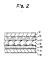
- Fig. 2 is an explanatory view for thoroughly explaining a concept that the liquid crystal layer is controlled by a synthetic electric field owing to the lines of electric force.
- the lines of electric force are spread from the transparent and fine electrodes the width of which is less than 50% of an electrode pitch.
- Reference numeral 12 denotes thick and transparent insulating layers arranged adjacent to the electrode 14 and 16 to sufficiently spread and make the lines of electric force uniform before the synthetic electric field is formed in the liquid crystal layer 11 having, for example, 180° twisted LC material 19.
- the lines of electric force shown with dotted lines are sufficiently spread in the insulating layers 20 and thus in the electric field of the liquid crystal 11(20) a degree of periodic modulation is reduced due to narrowness of the electrode width and interval of the electrodes.
- the liquid crystal material 20 is constructed so that a twist angle thereof is 180°.
- the 180° twisted structure is apparently similar to that of a non-twisted device in which a voltage sensitivity is high and a linearity of optical modulation characteristics for voltage is prominent. Because a sharpness of electric-optical characteristics in the liquid crystal increases due to twisting.
- An incident polarized light that oscillates in the oriented direction of a liquid crystal molecule is twisted and output by the twisted structure.
- a pixel electrode has applied there to a voltage greater than a threshold value and therefore the twisted structure of the liquid crystal adjacent to the pixel electrode is broken and is oriented in the perpendicular direction so that the incident light passes through the liquid crystal as it is.
- a twisted light and a directly passing light are in agreement on an oscillating face of a polarized light and in disagreement on only a phase. Therefore the liquid crystal may fulfill a function as a phase modulation device.
- the liquid crystal in which a twist is strengthened to integer multiples of 180° may be used.
- Fig. 3 is a diagram of a waveform of timing electrodes. References tp1, tp2 and tp3 shown in this figure indicate an example of a waveform of timing electrodes. if consideration is given to removing a picture regularity, polarity inversion of pixel driving in the liquid crystal is carried out for every line or every frame and further a regular switching thereof is carried out with random numbers. Thereby a polarity of neighboring timing electrodes becomes the same and a potential thereof at least holds a zero electric potential from a point of view of pixel fusion purposes.
- a symbol s11 shows an example of a waveform allowing all three pixels on three timing electrodes to turn on a light.
- Symbols s110 and s011 show an example of waveforms allowing two pixels on tow timing electrodes to turn on a light and a symbol s010 show an example of a waveform allowing one pixel on one timing electrode to turn on a light.
- a voltage applied to a liquid crystal pixel is a difference between voltages of timing electrodes tpi and si, and therefore the liquid crystal is driven based on an alternating effective value.
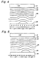
- Figs. 4 and 5 are schematic views which are useful for explaining the effect of improvement of pattern positional accuracy.
- Reference numeral 21 denotes an upper substrate made of a transparent dielectric
- reference numeral 29 denotes a lower substrate
- reference numerals 23 and 28 denote transparent electrodes formed on the surface of the substrates described above
- reference numerals 24 and 26 denote the section of the equipotential surfaces in Fig. 4
- reference numerals 34 and 36 denote the section of the equipotential surface in Fig. 5.
- Figs. 4 and 5 show the same liquid crystal device, and the only difference resides in the voltage pattern impressed on the electrodes.
- positional accuracy itself of the pattern is determined by the pitch of the fine electrodes independently of the thickness of the liquid crystal layer, and can be set more finely than the thickness of the liquid crystal layer.
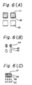
- Fig. 6 is an explanatory view useful for explaining a transverse electric field effect in the fine pixel group when the conditions 1.1 and 1.2 are simultaneously satisfied.
- the electrode dimension and the electrode gap are changed with the same thickness of the liquid crystal layer, and the mode of the distribution of the electric field in this case is shown.
- reference numerals 42 and 43 denote pixel electrode portions having the conventional dimension
- reference numeral 41 denotes the pixel shape when the electrode portion 42 is turned ON.
- the electric field of the portion 42 immediately below the electrode is substantially uniform overall, and only the peripheral portion is slightly weaker.
- Reference numeral 45 denotes the shape of the electrode portion when the electrode dimension is reduced while the electrode gap is maintained, under the condition of the same liquid crystal thickness and the same impressed voltage.
- Reference numeral 44 denotes the shape of the pixels when the electrode portion 45 is turned ON, and reference numeral 46 denotes the pixel gap. Since the electrode dimension is reduced while the gap is kept constant, the proportion of the area immediately below the electrode to the total area, that is, an aperture ratio, drops drastically because the condition (A) is changed to the condition (B). Furthermore, the ON range of the shape of the pixel 41 with respect to the electrode shape 42 becomes smaller than the electrode because the electric field around the peripheral portion becomes smaller. The ratio of the decrease of the area of the pixel 44 to the shape 45 of the electrode portion under the condition (B) is greater than the ratio of the decrease of the area of the pixel 41 to the shape 42 of the electrode portion under the condition (A).
- the first effect of the present invention resides in that a high aperture ratio is accomplished by miniaturizing the electrodes.
- the condition (C) in Fig. 6 is the one under which the electrode dimension of the condition (B) is further reduced so that "eating" of the electrodes becomes substantially 100%, and the gaps between the electrodes of the fine pixel electrodes are packed.
- the lines of electric force swell in the transverse direction and the electric field immediately below the electrodes becomes weaker. Nonetheless, the electric field at the gap portions of the electrodes is the vector sum of the surrounding electric fields, so that when all the surrounding electrodes are "ON", the electric field at the gap portions approaches "ON” and when all the surrounding electrodes are "OFF", the electric field at the gap portions approaches "OFF".
- the electric field can be impressed by reducing the gap.
- the electric field which is weakened by swelling of the lines of electric force,-too can be reinforced by reinforcing the impressed voltage.
- the liquid crystal immediately below the electrode that has been "eaten” nearly 100% by eating of the electrode can be turned ON, and furthermore, the pixels can be expanded and interconnected by increasing the impressed voltage, so that the liquid crystal of the electrode gaps can be driven.
- the problem of the drop of the aperture ratio that has been the critical problem with the fine pixel liquid crystal device can be solved by improving the aperture ratio. This effect is brought forth by interconnected driving of a plurality of fine pixels rather than by the thickness of the liquid crystal layer that was originally believed unnecessary.
- the second important effect of the present invention resides in that the present invention demonstrates the possibility of interconnecting a plurality of adjacent pixels and driving them in a driving condition as in the pixel forming electrode condition (C) shown in Fig. 4.
- the driving effect is limited even when each fine pixel is individually driven, but when a plurality of pixels are interconnected as shown in Fig. 4, the surrounding electrode groups as a whole inclusive of the gap regions indicated by reference numeral 48 can be turned OFF.
- the liquid crystal layer of this region eventually forms a continuous OFF region.
- the electrode 49 is turned ON, and an interconnected ON region pixel 47 inclusive of the neighboring gap 48 can be formed.
- Fig. 7 shows the electric field distribution in the case of interconnected driving of the pixels in the structure consisting of the fine pixel electrodes and the gaps.
- reference numerals 1101 and 1119 denote the upper and lower electrode substrates
- reference numeral 1102 denotes a common timing electrode
- reference numerals 1103 to 1112 denote segment electrodes formed on the surface of the lower substrate.
- An OFF voltage and an ON voltage are applied between the segment electrodes 1119 and 1111 having a great dimension and the opposed electrode 1102, respectively.
- the ON voltage is applied to the electrodes 1104, 1108, 1109, 1110, while the OFF voltage is applied to the electrodes 1103, 1105, 1106.
- the electric fields in the gaps can be connected smoothly to one another when the potential of the adjacent fine pixel electrodes is equal.
- Fig. 8 (A) and (B) are explanatory views useful for explaining the dimension of the pixels, positional accuracy of the resulting pattern, and the spatial noise component.
- reference numeral 51 denotes coarse pixel electrodes and reference numeral 52 denotes patterns that should be formed originally by the coarse pixels.
- reference numeral 53 denotes the fine electrodes
- reference numeral 54 denotes patterns that should be formed originally by the fine pixel electrodes.
- the difference between the patterns to be formed and the colored pixel portions correspond to the spatial noise component.
- the pitch of the coarse pixels 51 is substantially equal to the width and gap of the pattern to be formed, but reproduction of smooth patterns 52 becomes difficult in such a case.
- reproduction of similar patterns 54 becomes possible. It can thus be understood that miniaturization of the pixel electrodes is effective for the reproduction of a high precision hologram diffraction pattern.
- Fig. 9 shows a structure in which a two-terminal switching device is combined with buried electrodes
- Fig. 8 shows a wiring structure of Fig. 9.
- reference numeral 91 denotes an upper substrate
- reference numeral 99 denotes a lower substrate
- reference numeral 96 denotes.upper electrodes
- reference numeral 94 denotes lower electrode
- reference numeral 98 denotes metal-buried lead wires
- reference numeral 97 denotes a connection structure of the electrodes and the wirings utilizing the switching device.
- the substrates 91 and 99 are transparent glass substrates
- the electrodes 96 are transparent electrodes
- the wirings 98 are metal wirings of aluminum, tantalum, or the like.
- the glass substrate is first etched using hydrofluoric acid HF to form a thin metal film, and a thin insulating coating film by an oxide film or an organic thin film is formed on the thin metal film.
- a dielectric material to flatten the surface of the substrate, a contact hole is opened in the dielectric material, and connection is then made to the transparent electrode through the thin insulating film.
- reference numeral 106 denotes the buried metal wirings
- reference numeral 104 denotes the insulating film
- reference numeral 108 denotes a packing insulating material for surface flattening
- reference numeral 102 denotes the transparent electrode.
- the electrode 102 may be a metal or transparent electrode.
- the packing material 108 is necessary for flattening the substrate of the liquid crystal device having a fine structure.
- a film of tantalum oxide or aluminum oxide, or an organic film, can be used as the insulating film 104.
- the metal electrode 106, the insulating film 104 and the electrode 108 constitute an MIM (metal/insulator/metal) structure, and this structure functions as a two-terminal switching device. In other words, the switching device does not permit the passage of a current below a threshold voltage and rapidly allows the passage of the current beyond the threshold voltage. This operation can suppress cross-talk in driving.
- the passive buried electrode structure is a structure excluding the electrode 102, the insulating thin film 104 and the contact hole. This structure is much more simplified than an active switching type structure, and is more suitable for a finer structure.
- the present invention can now provide a definite method and structure of miniaturization of the pixels.
- a structure using a metal wire to secure electrical conductivity has significance.
- modulation of the liquid crystal layer can be carried out by exclusively utilizing the electric fields of the electrode gaps.
- Such a structure is particularly effective when a ferroelectric liquid crystal is used.
- a liquid crystal device in this case becomes a device having strong spontaneous polarization, a large current must be passed when the direction of the molecules is switched.
- a large number of fine pixels accomplishing the liquid crystal optical modulator device must be arranged in a matrix and be driven, but it is noteworthy that a high performance spatial optical modulator device utilizing a super-twist (STN) structure of a ferroelectric liquid crystal device (FLC) can be provided.
- the ferroelectric liquid crystal device can be driven at a liquid crystal layer thickness of not greater than 1.5 ⁇ m, and is a promising applicant for the miniaturization of the pixels.
- a structure which selectively drives the pixels by the combination with an active switching device becomes effective.
- Fig. 11 shows still another embodiment of the present invention which uses the liquid crystal modulator of this invention as a real-time diffraction device for electronic control so as to effect the control of a laser beam in a travelling direction, and a converging function.
- a system for scanning a laser beam is known which prints a hologram to a rotary disc as a holographic scanner, and which scans the laser beam by rotating this disc.
- Optical scanning devoid of any mechanical moving portion becomes possible by the pattern modification movement of the liquid crystal hologram through the rotation of the disc by the electronic control.
- one modulator device can exhibit this function, but it is possible to broaden the deflection angle of the beam and to improve optical utilization efficiency by combining a plurality of modulator devices.
- Fig. 11 shows still another embodiment of the present invention which uses the liquid crystal modulator of this invention as a real-time diffraction device for electronic control so as to effect the control of a laser beam in a travelling direction, and a converging function.
- reference numeral 62 denotes a laser beam source
- reference numerals 64 and 66 denote optical systems including lens for expanding the optical beams and for converting them to parallel beams
- reference numerals 68 and 69 denote the optical modulator devices according to the present invention
- reference numerals 63 and 65 denote control circuits including a driving signal source of the liquid crystal optical modulator device and a driving circuit for the signal
- reference numeral 61 denotes a converging point of the beam.
- the laser 62 may be a gas laser or a semiconductor laser, but the semiconductor laser is smaller in volume and effective.
- the liquid crystal optical modulator devices 68, 69 are electronically controlled by the signals of the control circuits 63, 65, and the direction of the laser beam are controlled.
- An opto-thermal-sensitive printer can be constituted by disposing heat-sensitive paper, a heat-sensitive ribbon and paper at the converging point of the beam, two-dimensionally scanning the beam and effecting condensation control.
- a complete solidi-state write/read mechanism to and from an optical disk memory or an optical card can be obtained by disposing an optical recording medium at the converging point 61 of the beam.
- a readout operation of an optical recording medium can be carried out by disposing a beam splitter between the lens 66 and the modulator device 68 in the same way as in the structure of the prior art, and detecting the return beam.
- the mechanical scanning mechanism of the prior art using a rotary mirror or an oscillating mirror can be converted to a complete solid-state or partially solid-state mechanism not having any mechanical moving portion, and the resulting system becomes superior to the prior art devices in the aspects of volume, weight and response speed.
- the liquid crystal optical modulator device can utilize the phase modulation and intensity modulation of the beam and the rotary modulation of the deflection plane by the liquid crystal device, or their combinations in various ways.
- Fig. 12 is an explanatory view useful for explaining the pattern position movement of the optical modulator device used in Fig. 11.
- reference numerals 75 and 76 denote the liquid crystal optical modulator devices
- reference numerals 73 and 74 denote examples of diffraction patterns formed by the liquid crystal devices
- reference numerals 77 and 78 denote masking patterns
- reference numerals 71 and 72 denote incident beams.
- the incident beam 71 leaving the lens 66 shown in Fig. 11 is diffracted by the diffraction pattern 73, the resulting diffracted beam becomes the incident beam 72 to the device 76, and this incident beam 72 is diffracted and condensed by the pattern 74 and is guided to 61.
- Fig. 13 shows a structural example of a stereoscopic television system using the liquid crystal device according to the present invention.
- Reference numeral 1210 denotes a laser beam source
- reference numeral 1240 denotes a beam splitter
- reference numerals 1242, 1244 and 1246 denote mirrors
- reference numerals 1212, 1213 and 1214 denote imaging devices
- reference numeral 1216 denotes a signal synthesizer
- reference numeral 1218 denotes a transmission line
- reference numeral 1220 denotes the optical modulator device according to the present invention
- reference numeral 1222 denotes a laser beam source
- reference numeral 1224 denotes a spatial filter comprised of the liquid crystal device.
- the beam is reflected, on one hand, by the mirrors 1242, 1244, 1246 and converted to reference beams.
- the reference beams are guided to the device inside the imaging devices 1212, 1213, 1214.
- a plurality of holograms are formed on the imaging devices, and their results are made into a composite. Unnecessary stray beams are cut off by the use of the spatial filter, whenever necessary. This can be controlled electronically, too, by using the liquid crystal, and flexibility to cope with varying situations can be enhanced.
- the use of a plurality of imaging devices is effective for enlarging the visual field as well as for collecting color data. Though only one imaging device is shown in the drawing, a plurality of optical modulator devices for reproduction are also juxtaposed and are effectively utilized to improve the visual field of the reproduced image and to impart colors.
- Fig. 14 shows the arrangement of pixels of a multi-imaging device for improving fineness in three-dimensional imaging.
- Reference numeral 810 denotes a beam splitter
- reference numeral 812 denotes an imaging device which collects a screen consisting of a set of pixels A
- reference numeral 814 denotes an imaging device which collects a screen consisting of a set of pixels B
- reference numeral 816 denotes an image obtained by combining both A and B.
- the images 812 and 814 which are different by only a bit from each other are collected by the economical imaging device from the images split by the beam splitter, and a very fine image 816 is synthesized from the superposition of the image data and is utilized for the reproduction of the image.
Claims (3)
- Verfahren zur Erzeugung eines Beugungsmusters, das umfasst: Bereitstellen eines optischen Modulatorbauelements, wobei das optische Modulatorbauelement beinhaltet:wobei die Breite (W) der feinen Elektroden und der Zwischenraumabstand (S) zwischen den feinen Elektroden jeweils kleiner als die Dicke (H) der dazwischen geschichteten Flüssigkristallschicht ist;ein Paar transparenter, isolierender Substrate (12, 18) mit gegenüberliegenden Oberflächen;zwei orthogonale Gruppen von unabhängig steuerbaren, parallelen und gleichmäßig beabstandeten, streifenförmigen, feinen Elektroden (14, 16), wobei eine Gruppe auf einer Oberfläche von einem der transparenten, isolierenden Substrate angeordnet ist und die andere Gruppe auf der gegenüberliegenden Oberfläche des anderen der isolierenden Substrate angeordnet ist, so dass sie einander gegenüberliegen; undeine Flüssigkristallschicht (19), die zwischen die gegenüberliegenden Oberflächen des Paars der transparenten, isolierenden Substrate geschichtet ist und durch die Elektroden elektrisch angesteuert wird;
wobei das Verfahren ein Ansteuern einer Mehrzahl unmittelbar benachbarter feiner Elektroden (1108 bis 1111) beinhaltet, indem die gleiche Spannung an dieselben in einer jeweiligen Ansteuerphase angelegt wird, um so ein Gebiet der Flüssigkristallschicht, das sich direkt unter der Mehrzahl von Elektroden erstreckt, mit der gleichen Spannung anzusteuern, um ein entsprechendes kontinuierliches räumliches Muster (54, 55) zu bilden, wobei die Elektroden der einen Gruppe zeitlich nacheinander (tp1, tp2 und tp3) angesteuert werden und die Elektroden der anderen Gruppe gleichzeitig (S111, S110, S010 und S011) angesteuert werden. - Verfahren nach Anspruch 1, wobei die Flüssigkristalldünnschicht durch ein zusammengesetztes elektrisches Feld angesteuert wird, das durch Potentiale von Elektroden bewirkt wird, die auf den Substraten durch eine MIM-Struktur mit Metalldrähten (98, 106), die in dem Substrat vergraben sind, einem isolierenden Film (104) und den Elektroden gebildet sind.
- Verfahren nach Anspruch 1 oder 2, wobei eine glatte Potentialverteilung durch verteilendes Ausbreiten der elektrischen Kraftlinien mittels Bedecken der Substrate durch eine transparente isolierende Schicht (20) erreicht wird, welche die Elektroden (14, 16) von der Flüssigkristallschicht (19) trennt.
Priority Applications (3)
| Application Number | Priority Date | Filing Date | Title |
|---|---|---|---|
| EP93101362A EP0608458B1 (de) | 1993-01-29 | 1993-01-29 | Verfahren zur Steuerung einer optischen Modulationsvorrichtung |
| DE1993631410 DE69331410T2 (de) | 1993-01-29 | 1993-01-29 | Verfahren zur Steuerung einer optischen Modulationsvorrichtung |
| US08/396,052 US5654782A (en) | 1993-01-29 | 1995-02-28 | Liquid crystal optical modulator device with each electrode width smaller than both the liquid crystal thickness and the electrode gaps |
Applications Claiming Priority (2)
| Application Number | Priority Date | Filing Date | Title |
|---|---|---|---|
| EP93101362A EP0608458B1 (de) | 1993-01-29 | 1993-01-29 | Verfahren zur Steuerung einer optischen Modulationsvorrichtung |
| US08/396,052 US5654782A (en) | 1993-01-29 | 1995-02-28 | Liquid crystal optical modulator device with each electrode width smaller than both the liquid crystal thickness and the electrode gaps |
Publications (2)
| Publication Number | Publication Date |
|---|---|
| EP0608458A1 EP0608458A1 (de) | 1994-08-03 |
| EP0608458B1 true EP0608458B1 (de) | 2002-01-02 |
Family
ID=26133066
Family Applications (1)
| Application Number | Title | Priority Date | Filing Date |
|---|---|---|---|
| EP93101362A Expired - Lifetime EP0608458B1 (de) | 1993-01-29 | 1993-01-29 | Verfahren zur Steuerung einer optischen Modulationsvorrichtung |
Country Status (2)
| Country | Link |
|---|---|
| US (1) | US5654782A (de) |
| EP (1) | EP0608458B1 (de) |
Families Citing this family (25)
| Publication number | Priority date | Publication date | Assignee | Title |
|---|---|---|---|---|
| JP3379671B2 (ja) * | 1995-05-23 | 2003-02-24 | 富士通株式会社 | 光偏向装置 |
| GB2315902A (en) * | 1996-08-01 | 1998-02-11 | Sharp Kk | LIquid crystal device |
| TW434443B (en) * | 1997-05-30 | 2001-05-16 | Samsung Electronics Co Ltd | Liquid crystal display |
| US6704083B1 (en) * | 1997-05-30 | 2004-03-09 | Samsung Electronics, Co., Ltd. | Liquid crystal display including polarizing plate having polarizing directions neither parallel nor perpendicular to average alignment direction of molecules |
| US5907380A (en) * | 1997-10-30 | 1999-05-25 | International Business Machines Corporation | Liquid crystal cell employing thin wall for pre-tilt control |
| US6052165A (en) * | 1997-12-22 | 2000-04-18 | Philips Electronics North America Corporation | Reflective liquid crystal display (LCD) device having an internal reflection reducer |
| JP2000089364A (ja) * | 1998-09-09 | 2000-03-31 | Seiko Epson Corp | 光変調装置およびこの光変調装置を利用した投写型表示装置 |
| US6788722B1 (en) * | 2000-07-10 | 2004-09-07 | Coherent, Inc. | High power waveguide laser |
| US6697408B2 (en) | 2001-04-04 | 2004-02-24 | Coherent, Inc. | Q-switched cavity dumped CO2 laser for material processing |
| US6826204B2 (en) * | 2001-04-04 | 2004-11-30 | Coherent, Inc. | Q-switched CO2 laser for material processing |
| TW528636B (en) * | 2001-05-09 | 2003-04-21 | Electro Scient Ind Inc | Micromachining with high-energy, intra-cavity Q-switched CO2 laser pulses |
| JP3873827B2 (ja) * | 2001-07-26 | 2007-01-31 | セイコーエプソン株式会社 | 液晶装置及び電子機器 |
| US6701605B2 (en) | 2001-10-09 | 2004-03-09 | Sonoco Development, Inc. | Conductive electrical element and antenna with ink additive technology |
| US7131380B2 (en) * | 2001-11-07 | 2006-11-07 | Sonoco Development, Inc. | EB pattern profile printing |
| KR20040013753A (ko) * | 2002-08-08 | 2004-02-14 | 삼성전자주식회사 | 기판 및 이를 포함하는 액정 표시 장치 |
| US7039079B2 (en) * | 2003-03-14 | 2006-05-02 | Coherent, Inc. | Pulsed CO2 laser including an optical damage resistant electro-optical switching arrangement |
| EP1743211A4 (de) * | 2004-04-13 | 2007-11-07 | Univ Arizona | Strukturierte elektroden für elektroaktive flüssigkristall-augenoptikeinrichtungen |
| TWI363903B (en) * | 2005-11-04 | 2012-05-11 | Hon Hai Prec Ind Co Ltd | Colour-disparting element and liquid crystal display |
| US20070159574A1 (en) * | 2006-01-06 | 2007-07-12 | Eastman Kodak Company | Common transparent electrode for reduced voltage displays |
| WO2007089094A1 (en) * | 2006-01-31 | 2007-08-09 | Sang-Up Park | Flat light source minimized fraunhofer diffraction |
| JP4524689B2 (ja) * | 2007-02-20 | 2010-08-18 | ソニー株式会社 | ホログラム再生装置およびホログラム再生方法並びに位相変調素子 |
| KR101832265B1 (ko) | 2011-11-24 | 2018-02-26 | 삼성전자주식회사 | 능동 광학 소자 및 이를 포함하는 디스플레이 장치 |
| KR101996655B1 (ko) * | 2012-12-26 | 2019-07-05 | 엘지디스플레이 주식회사 | 홀로그램 표시 장치 |
| CN109073939A (zh) * | 2016-03-25 | 2018-12-21 | 赛伊视觉公司 | 提供增强的观看体验的近眼图像显示设备 |
| KR20180052357A (ko) * | 2016-11-10 | 2018-05-18 | 삼성전자주식회사 | 확장된 시야창을 제공하는 홀로그래픽 디스플레이 장치 |
Family Cites Families (6)
| Publication number | Priority date | Publication date | Assignee | Title |
|---|---|---|---|---|
| US4542960A (en) * | 1982-06-30 | 1985-09-24 | International Business Machines Corporation | Fringe-field switched storage-effect liquid crystal display devices |
| FR2541784B1 (fr) * | 1983-02-25 | 1986-05-16 | Thomson Csf | Dispositif de deflexion statique d'un faisceau infra-rouge |
| US5122888A (en) * | 1987-07-10 | 1992-06-16 | Canon Kabushiki Kaisha | Focusing plate having phase grating formed by using liquid crystal |
| US5136409A (en) * | 1987-09-29 | 1992-08-04 | Canon Kabushiki Kaisha | Liquid crystal device having at least two zones having different diffusion characteristics |
| US5056895A (en) * | 1990-05-21 | 1991-10-15 | Greyhawk Systems, Inc. | Active matrix liquid crystal liquid crystal light valve including a dielectric mirror upon a leveling layer and having fringing fields |
| US5093740A (en) * | 1991-02-28 | 1992-03-03 | Raytheon Company | Optical beam steerer having subaperture addressing |
-
1993
- 1993-01-29 EP EP93101362A patent/EP0608458B1/de not_active Expired - Lifetime
-
1995
- 1995-02-28 US US08/396,052 patent/US5654782A/en not_active Expired - Lifetime
Also Published As
| Publication number | Publication date |
|---|---|
| EP0608458A1 (de) | 1994-08-03 |
| US5654782A (en) | 1997-08-05 |
Similar Documents
| Publication | Publication Date | Title |
|---|---|---|
| EP0608458B1 (de) | Verfahren zur Steuerung einer optischen Modulationsvorrichtung | |
| US6297899B1 (en) | Discrete element light modulating microstructure devices | |
| JP4084203B2 (ja) | 光偏向装置 | |
| EP0356174B1 (de) | Wiedergabegerät für ein Ladungslatentbildaufzeichnungsmedium | |
| EP0811872A1 (de) | Mit Lichtbeugung arbeitender räumlicher Lichtmodulator und Anzeigevorrichtung | |
| US20040212550A1 (en) | Three-dimensional volumetric display | |
| JP2000217053A (ja) | 回折空間光変調器およびディスプレイ | |
| US20050179681A1 (en) | Optical switching element, and switching device and image display apparatus each using the optical switching element | |
| US5596430A (en) | Distributed index light deflector and method of light deflection | |
| US4480899A (en) | Two dimensional electro-optic modulator and applications therefor | |
| US5786926A (en) | Electro-optical device having inverted domains formed inside a ferro-electric substrate and electro-optical unit utilizing thereof | |
| JP4717087B2 (ja) | 光偏向装置 | |
| US5291566A (en) | Total internal reflection electro-optic modulator for multiple axis and asymmetric beam profile modulation | |
| US6486996B1 (en) | Discrete element light modulating microstructure devices | |
| KR100425682B1 (ko) | 공간 광변조 어레이 제조방법 및 이를 이용한 레이저 표시장치 | |
| JP3270075B2 (ja) | 光変調素子 | |
| CN100595629C (zh) | 桥式光栅光调制器及其阵列 | |
| JPH10206756A (ja) | 光記録装置 | |
| JPH10206885A (ja) | 光記録装置 | |
| JPS58106590A (ja) | ポジ型液晶ライトバルブ | |
| JPH01500697A (ja) | 光偏向装置及びその方法 | |
| JPH08220497A (ja) | 光スイッチおよびこれを用いた光走査装置 | |
| JPS6254217A (ja) | 画像シフト装置 | |
| JPH0527089B2 (de) | ||
| JPH05142514A (ja) | 光スイツチング装置 |
Legal Events
| Date | Code | Title | Description |
|---|---|---|---|
| PUAI | Public reference made under article 153(3) epc to a published international application that has entered the european phase |
Free format text: ORIGINAL CODE: 0009012 |
|
| AK | Designated contracting states |
Kind code of ref document: A1 Designated state(s): DE FR GB |
|
| 17P | Request for examination filed |
Effective date: 19950128 |
|
| 17Q | First examination report despatched |
Effective date: 19970702 |
|
| GRAG | Despatch of communication of intention to grant |
Free format text: ORIGINAL CODE: EPIDOS AGRA |
|
| RTI1 | Title (correction) |
Free format text: A METHOD OF OPERATING AN OPTICAL MODULATOR DEVICE |
|
| RTI1 | Title (correction) |
Free format text: A METHOD OF OPERATING AN OPTICAL MODULATOR DEVICE |
|
| GRAG | Despatch of communication of intention to grant |
Free format text: ORIGINAL CODE: EPIDOS AGRA |
|
| GRAH | Despatch of communication of intention to grant a patent |
Free format text: ORIGINAL CODE: EPIDOS IGRA |
|
| GRAH | Despatch of communication of intention to grant a patent |
Free format text: ORIGINAL CODE: EPIDOS IGRA |
|
| GRAA | (expected) grant |
Free format text: ORIGINAL CODE: 0009210 |
|
| RAP1 | Party data changed (applicant data changed or rights of an application transferred) |
Owner name: CITIZEN WATCH CO. LTD. |
|
| REG | Reference to a national code |
Ref country code: GB Ref legal event code: IF02 |
|
| AK | Designated contracting states |
Kind code of ref document: B1 Designated state(s): DE FR GB |
|
| REF | Corresponds to: |
Ref document number: 69331410 Country of ref document: DE Date of ref document: 20020207 |
|
| ET | Fr: translation filed | ||
| PLBE | No opposition filed within time limit |
Free format text: ORIGINAL CODE: 0009261 |
|
| STAA | Information on the status of an ep patent application or granted ep patent |
Free format text: STATUS: NO OPPOSITION FILED WITHIN TIME LIMIT |
|
| 26N | No opposition filed | ||
| PGFP | Annual fee paid to national office [announced via postgrant information from national office to epo] |
Ref country code: FR Payment date: 20060110 Year of fee payment: 14 |
|
| PGFP | Annual fee paid to national office [announced via postgrant information from national office to epo] |
Ref country code: GB Payment date: 20060125 Year of fee payment: 14 |
|
| PGFP | Annual fee paid to national office [announced via postgrant information from national office to epo] |
Ref country code: DE Payment date: 20060126 Year of fee payment: 14 |
|
| PG25 | Lapsed in a contracting state [announced via postgrant information from national office to epo] |
Ref country code: DE Free format text: LAPSE BECAUSE OF NON-PAYMENT OF DUE FEES Effective date: 20070801 |
|
| GBPC | Gb: european patent ceased through non-payment of renewal fee |
Effective date: 20070129 |
|
| REG | Reference to a national code |
Ref country code: FR Ref legal event code: ST Effective date: 20070930 |
|
| PG25 | Lapsed in a contracting state [announced via postgrant information from national office to epo] |
Ref country code: GB Free format text: LAPSE BECAUSE OF NON-PAYMENT OF DUE FEES Effective date: 20070129 |
|
| PG25 | Lapsed in a contracting state [announced via postgrant information from national office to epo] |
Ref country code: FR Free format text: LAPSE BECAUSE OF NON-PAYMENT OF DUE FEES Effective date: 20070131 |