EP0603667A2 - Connecteur de communication avec condensateur multicouche - Google Patents
Connecteur de communication avec condensateur multicouche Download PDFInfo
- Publication number
- EP0603667A2 EP0603667A2 EP93119879A EP93119879A EP0603667A2 EP 0603667 A2 EP0603667 A2 EP 0603667A2 EP 93119879 A EP93119879 A EP 93119879A EP 93119879 A EP93119879 A EP 93119879A EP 0603667 A2 EP0603667 A2 EP 0603667A2
- Authority
- EP
- European Patent Office
- Prior art keywords
- conductive
- contact
- lamina
- set forth
- connector
- Prior art date
- Legal status (The legal status is an assumption and is not a legal conclusion. Google has not performed a legal analysis and makes no representation as to the accuracy of the status listed.)
- Granted
Links
Images


Classifications
-
- H—ELECTRICITY
- H01—ELECTRIC ELEMENTS
- H01R—ELECTRICALLY-CONDUCTIVE CONNECTIONS; STRUCTURAL ASSOCIATIONS OF A PLURALITY OF MUTUALLY-INSULATED ELECTRICAL CONNECTING ELEMENTS; COUPLING DEVICES; CURRENT COLLECTORS
- H01R13/00—Details of coupling devices of the kinds covered by groups H01R12/70 or H01R24/00 - H01R33/00
- H01R13/66—Structural association with built-in electrical component
- H01R13/719—Structural association with built-in electrical component specially adapted for high frequency, e.g. with filters
- H01R13/7195—Structural association with built-in electrical component specially adapted for high frequency, e.g. with filters with planar filters with openings for contacts
-
- H—ELECTRICITY
- H01—ELECTRIC ELEMENTS
- H01R—ELECTRICALLY-CONDUCTIVE CONNECTIONS; STRUCTURAL ASSOCIATIONS OF A PLURALITY OF MUTUALLY-INSULATED ELECTRICAL CONNECTING ELEMENTS; COUPLING DEVICES; CURRENT COLLECTORS
- H01R13/00—Details of coupling devices of the kinds covered by groups H01R12/70 or H01R24/00 - H01R33/00
- H01R13/646—Details of coupling devices of the kinds covered by groups H01R12/70 or H01R24/00 - H01R33/00 specially adapted for high-frequency, e.g. structures providing an impedance match or phase match
- H01R13/6461—Means for preventing cross-talk
- H01R13/6464—Means for preventing cross-talk by adding capacitive elements
-
- H—ELECTRICITY
- H01—ELECTRIC ELEMENTS
- H01R—ELECTRICALLY-CONDUCTIVE CONNECTIONS; STRUCTURAL ASSOCIATIONS OF A PLURALITY OF MUTUALLY-INSULATED ELECTRICAL CONNECTING ELEMENTS; COUPLING DEVICES; CURRENT COLLECTORS
- H01R13/00—Details of coupling devices of the kinds covered by groups H01R12/70 or H01R24/00 - H01R33/00
- H01R13/66—Structural association with built-in electrical component
- H01R13/6608—Structural association with built-in electrical component with built-in single component
- H01R13/6625—Structural association with built-in electrical component with built-in single component with capacitive component
-
- H—ELECTRICITY
- H01—ELECTRIC ELEMENTS
- H01R—ELECTRICALLY-CONDUCTIVE CONNECTIONS; STRUCTURAL ASSOCIATIONS OF A PLURALITY OF MUTUALLY-INSULATED ELECTRICAL CONNECTING ELEMENTS; COUPLING DEVICES; CURRENT COLLECTORS
- H01R24/00—Two-part coupling devices, or either of their cooperating parts, characterised by their overall structure
- H01R24/60—Contacts spaced along planar side wall transverse to longitudinal axis of engagement
- H01R24/62—Sliding engagements with one side only, e.g. modular jack coupling devices
- H01R24/64—Sliding engagements with one side only, e.g. modular jack coupling devices for high frequency, e.g. RJ 45
-
- Y—GENERAL TAGGING OF NEW TECHNOLOGICAL DEVELOPMENTS; GENERAL TAGGING OF CROSS-SECTIONAL TECHNOLOGIES SPANNING OVER SEVERAL SECTIONS OF THE IPC; TECHNICAL SUBJECTS COVERED BY FORMER USPC CROSS-REFERENCE ART COLLECTIONS [XRACs] AND DIGESTS
- Y10—TECHNICAL SUBJECTS COVERED BY FORMER USPC
- Y10S—TECHNICAL SUBJECTS COVERED BY FORMER USPC CROSS-REFERENCE ART COLLECTIONS [XRACs] AND DIGESTS
- Y10S439/00—Electrical connectors
- Y10S439/941—Crosstalk suppression
-
- Y—GENERAL TAGGING OF NEW TECHNOLOGICAL DEVELOPMENTS; GENERAL TAGGING OF CROSS-SECTIONAL TECHNOLOGIES SPANNING OVER SEVERAL SECTIONS OF THE IPC; TECHNICAL SUBJECTS COVERED BY FORMER USPC CROSS-REFERENCE ART COLLECTIONS [XRACs] AND DIGESTS
- Y10—TECHNICAL SUBJECTS COVERED BY FORMER USPC
- Y10T—TECHNICAL SUBJECTS COVERED BY FORMER US CLASSIFICATION
- Y10T29/00—Metal working
- Y10T29/43—Electric condenser making
- Y10T29/435—Solid dielectric type
-
- Y—GENERAL TAGGING OF NEW TECHNOLOGICAL DEVELOPMENTS; GENERAL TAGGING OF CROSS-SECTIONAL TECHNOLOGIES SPANNING OVER SEVERAL SECTIONS OF THE IPC; TECHNICAL SUBJECTS COVERED BY FORMER USPC CROSS-REFERENCE ART COLLECTIONS [XRACs] AND DIGESTS
- Y10—TECHNICAL SUBJECTS COVERED BY FORMER USPC
- Y10T—TECHNICAL SUBJECTS COVERED BY FORMER US CLASSIFICATION
- Y10T29/00—Metal working
- Y10T29/49—Method of mechanical manufacture
- Y10T29/49002—Electrical device making
- Y10T29/49082—Resistor making
- Y10T29/49099—Coating resistive material on a base
Definitions
- the present invention relates generally to modular communication connectors used to interconnect computers through twisted pairs of telephone wires for high speed digital signal transmission, and more specifically relates to modular communication connectors having means for reducing near end cross talk between the contacts of each connector.
- a printed circuit board telephone jack connector that utilizes tombstone capacitors connected between each contact and a ground plane for bypassing noise and high frequency signals to ground is suggested in U.S. Patent No. 4,695,115. Also see U.S. Patent No. 4,772,224 which suggests a similar modular printed circuit board jack that utilizes parallelepiped capacitors in a similar manner. Both of these connectors require an electrical grounding path connected to each capacitor of each contact, comprising a conductive cover member that is soldered to the ground of a printed circuit board.
- a communication connector in general includes a plurality of contact pairs for conductive connection to respective communication signal wire pairs where a capacitor label is provided to capacitively couple a first contact of one contact pair to a second contact of a second contact pair to improve near end cross talk performance.
- a common conductive lamina disposed closely adjacent to and spaced from more than one of the contacts further enhances near end cross talk performance of the connector.
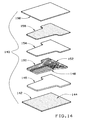
- a first embodiment of a capacitor label specially designed for application to a modular communication connector is designated generally by the numeral 20 in Figs. 1-8 in the accompanying drawings.
- the various layers depicted in the accompanying drawings are shown with increased thickness out of proportion to the surface of the label for clarity, the actual thickness of the layers varying from 0.0005 inch (0.0013 cm) to 0.003 inch (0.0076 cm).
- Capacitor Label 20 is formed by the assembly of a plurality of layers of insulating and conductive materials adhesively joined together.
- Printed on an insulating substrate 22 is a C3 conductive lamina 24.
- Insulating substrate 22 is preferably constructed of 0.001 to 0.003 inch (0.0025 - 0.0076 cm) thick layer of polyimide material, for example, Dupont's Kapton TM polyimide.
- Forward conductive lamina 28 and C1, C3, C5 and C7 conductive laminas 24, 30, 32 and 34 are preferably constructed of a 0.001 inch (0.0025 cm) thick layer of conductive silver ink, for example, Dupont's "5007" silver ink or Colonial's "E8205" silver ink.
- Conductive laminas can also be formed of conductive metal foils, such as a 0.002 inch (0.0051 cm) copper foil.
- a sheet of copper foil can be laminated to an insulating layer and then etched by either a wet or dry process to form the desired contours of the individual conductive laminas.
- a notch 36 is formed in dielectric layer 26, allowing access to C3 conductive lamina 24.
- Dielectric layer 26 extends over C3 conductive lamina 24 separating C1, C5 and C7 laminas 30, 32 and 34 from C3 conductive lamina 24 such that lamina 24 and each of conductive laminas 30, 32 and 34 are capacitively coupled.
- the overlapping area of each conductive lamina 30, 32 and 34 relative to C3 conductive lamina 24, the distance between the same, the properties of the dielectric separating the same and the properties of the conductive lamina all affect the amount of capacitance produced across each pair of capacitively coupled lamina.
- Dielectric layer 26 is adhesively secured to substrate 22 by a 0.0005 inch (0.0013 cm) thick adhesive lamina 38 preferably of an acrylic adhesive, for example Minnesota Mining and Manufacturing Company's "3M T "" 467" adhesive. Other alternative adhesives are ultraviolet curable adhesives or silicone adhesives.
- a 0.001 inch (0.0025 cm) thick Kapton TM polyimide insulating layer 40 is secured to dielectric layer 26 and the conductive lamina carried thereon by an adhesive lamina 42.
- An upper adhesive lamina 44 is carried on the upper surface of insulating layer 40.
- Adhesive laminas 42 and 44 are each formed of a 0.0005 inch (0.0013 cm) thick layer of acrylic adhesive identical to adhesive lamina 38.
- Conductive adhesive areas 46 are positioned on the respective surfaces of C1, C3, C5 and C7 conductive laminas 24, 30, 32 and 34.
- Release paper 48 which is preferably 3M's brand of high strength release paper, is releasably secured to insulating layer 40 by adhesive lamina 44.
- Label 20 is specially constructed for application to a modular communication connector which includes a housing 50, wire positioning fixture 52 and contact carrier 54. See U.S. Patent No. 5,118,310 assigned to common assignee Panduit Corp., which is incorporated herein by reference, for a more detailed description of the modular connector.
- Contact carrier 54 positions a plurality of contacts 56 each having an insulation displacement portion 58. As seen in Fig. 7, contacts 56 are positioned within a recess 60 of contact carrier 54. Label 20 is shaped to fit within recess 60. Label 20 is adhesively secured to contacts 56 by adhesive lamina 44 and is conductively secured to selective contacts 56 by conductive adhesive areas 46.
- Conductive adhesive areas 46 preferably are either areas of conductive adhesive transfer tape as depicted in Figs. 1, 2, 3, 5 and 8, such as 3M's Scotch TM 9703 anisotropic conductive adhesive transfer tape having conductive silver coated particles or of liquid drops of silver filled epoxy adhesive, which cure at room temperature, one example being Emerson and Cuming's Amicon" CSM 933-65-1 adhesive.
- Printed carbon filled adhesive areas are a less desirable alternative.
- 3M's anisotropic conductive adhesive tape conducts electricity only through the thickness of the tape and thus may also be applied as a single piece that is positioned between and adhered to all of the contacts that are to be conductively connected and the conductive laminas to which the contacts are to be respectively connected.
- the application of a single adhesive area in this manner should reduce the complexity of assembly and cost of manufacture of the communication connector.
- Another method of conductively engaging contacts 56 with conductive lamina in any of the relevant embodiments of the present invention include forming the housing and contacts such that the housing resiliently biases each contact into conductive engagement with a respective conductive lamina.
- the contact may also be held in conductive engagement with a respective conductive lamina by a fixture and then permanently secured thereto by a non-conductive adhesive.
- Copper foil conductive laminas can also either be soldered or microwelded to respective contacts.
- Fig. 8 schematically depicts the positional relationship of contacts C1 through C8, C1, C3, C5 and C7 conductive laminas 30, 24, 32 and 34 and conductive adhesive areas 46, with these components stacked in reverse order for clarity.
- Adhesive areas 46 respectively connect contact C1 to C1 conductive lamina 30, contact C3 to C3 conductive lamina 24, contact C5 to C5 conductive lamina 32 and contact C7 to C7 conductive lamina 34.
- C1 through C8 contacts define a standard communication connector for termination of four pair of twisted wires, contacts C1 and C2, contacts C3 and C6, contacts C4 and C5 and contacts C7 and C8 each comprising a signal pair.
- wire positioning fixture 52 includes a latch 62 that secures fixture 52 to housing 50.
- Fixture 52 includes a wire entry end 64 and a plurality of wire exit slots 66.
- a cable 68 includes a plurality of twisted pairs of wires designated W1 through W8.
- wires W1 and W2, wires W3 and W6, wires W4 and W5, and wires W7 and W8 each comprise a pair of twisted wires the terminal ends of which are straightened, positioned in wire positioning fixture 52, disposed adjacent to respective contacts and terminated to corresponding contacts C1 through C8.
- the terminal ends of wires W4 and W5 are twisted around each other one complete turn before insertion into fixture 52, as seen in Fig. 9, which has been found to further improve the near end cross talk performance of the communication connector of Fig. 6.
- the specific pair of terminally twisted wires W1 through W8 that will enhance performance may vary depending upon the wiring pair scheme of the connector and cable.
- the preferred configuration and approximate desired capacitance between each coupled contact for a connector having the contact signal pairs described above is to capacitively couple contacts C1, C5 and C7 to contact C3 with respective capacitance's of 2.1 pF, 8.5 pF and 2.1 pF.
- a second arrangement of equal performance is capacitively couple contacts C3 and C5, C3 and C7, and C2 and C6 with respective capacitance of 5.9 pF, 1.9 pF and 1.9 pF.
- Another arrangement of expected equal performance would be to capacitively couple contacts C2, C4 and C8 each to contact C6 with respective capacitance's of 2.1 pF, 8.5 pF and 2.1 pF.
- forward conductive lamina 28 which is disposed closely adjacent to and covering the forward portion of contacts C1 - C8. See Fig. 3, which discloses the full extent of forward conductive lamina 28.
- Forward conductive lamina 28 as depicted in Figs. 1-8 is a planar layer disposed adjacent contacts 56 which is believed to reduce cross talk between contact pairs by disrupting the coupled field between contacts reducing the field strength and reducing cross talk.
- An alternative disposition of lamina 28 includes weaving the conductive lamina, while separated from the contacts by a dielectric, over and under adjacent contacts 56 which is even more effective than a planar conductive lamina, although more difficult to manufacture.
- Forward conductive lamina 28 can also be placed between contacts 56 and contact carrier 54, or in any other disposition closely adjacent contacts 56.
- the forward conductive lamina is spaced closely adjacent the contacts and, thus, has a significant effect when it is within 0.005 inch (0.0127 cm) of the contacts, although the exact range will vary with different conductive lamina and contact configurations.
- Label 20 applied to a communication connector as described above achieves the highest category 5, TIA/EIA TSB40 level of performance.
- a capacitor label constructed with only a forward conductive lamina 28 or with only C1, C3, C5 and C7 conductive laminas 24, 30, 32 and 34 improves the cross talk performance of a communication connector.
- a second embodiment of the present invention is a printed capacitor label 70 specially designed for application to a modular communication connector of Figs. 6-8.
- the contours of the components of label 70 are identical to label 20 and label 70 is secured to the modular connector of Figs. 6-8 in an identical manner.
- Printed capacitor label 70 is formed by printing a plurality of layers of insulating and conductive materials on a substrate with label 70 being releasably attached to a pre-mask layer 72 by adhesive layer 74.
- Pre-mask layer 72 functions as a fixture allowing accurate fine manipulation and alignment of label 70 for application to the contacts of a connector.
- Pre-mask layer 72 is constructed of a 0.003 inch (0.0076 cm) layer of polyester film having an acrylic temporary low tack adhesive applied to one surface.
- pre-mask 72 would position a matrix of a plurality of labels 70 such that pre-mask 70, when aligned with a second fixture (not shown) that positions a plurality of contact carriers 54, would be used to apply a plurality of labels to individual contact carriers.
- An insulating substrate 76 is releasably secured to pre-mask 72. All of the subsequent layers of label 70, including insulating layers are printed sequentially on substrate 76.
- Printed on substrate 76 in the following order are a C3 conductive lamina 78; a printed dielectric lamina 80 having a notch 82 allowing conductive access to lamina 78; forward conductive lamina 84, C1 conductive lamina 86, C5 conductive lamina 88, and C7 conductive lamina 90; printed insulating lamina 92; and adhesive lamina 94.
- a standard release paper layer 96 is then applied to cover adhesive lamina 94.
- drops of liquid adhesive 98 are applied to portions of C1, C3, C5 and C7 conductive lamina 86, 78, 88 and 90 in alignment with each respective contact of the connector.
- Substrate 76 is preferably constructed of 0.001 to 0.002 inch (0.0025 - 0.0051 cm) thick layer of polyimide material, for example, Dupont's Kapton TM polyimide.
- Conductive lamina 78, 84, 86, 88 and 90 are printed layers of 0.001 inch (0.0025 cm) thick layer of conductive silver ink, for example, Dupont's "5007” silver ink or Colonial's "E8205" silver ink.
- Conductive laminas can also be formed of conductive metal foils, such as 0.002 inch (0.0051 cm) copper foil.
- Printed dielectric and insulating layers 80 and 92 are printed layers of 0.0018 inch (0.0046 cm) thick polymeric dielectric, for example DuPont's "5014D” polymeric dielectric or Minico's "M-UVF-10G” ultraviolet polymer solder mask.
- Liquid adhesive drops 98 are preferably liquid drops of silver filled epoxy adhesive, which cures at room temperature, one example being Emerson and Cuming's Amicon" CSM 933-65-1 adhesive.
- Dielectric layer 80 extends over C3 conductive lamina 78 separating C1, C5 and C7 laminas 86, 88 and 90 from C3 conductive lamina 24 such that lamina 78 and each of conductive laminas 86, 88 and 90 are capacitively coupled.
- the areas of each of C1, C5 and C7 conductive laminas 86, 88 and 98 that overlap C3 conductive lamina 78 are respectively 0.003 square inches (0.0194 square cm), 0.012 square inches (0.0774 square cm) and 0.003 square inches (0.0194 square cm).
- the capacitance values measured between the C1, C5 and C7 conductive laminas and the C3 conductive laminas are respectively 2.4 pF, 8.5 pF and 1.9 pF.
- a third embodiment of the present invention is a single point of contact capacitor label 100 specially designed for application to a modular communication connector of Figs. 6-8.
- label 100 will be effective in suppressing near end cross talk, it has not been found to achieve as high a level of performance as labels 20 and 70, but does offer an alternative construction that may be more desirable where the highest level of performance is not necessary.
- Label 100 is secured to the modular connector of Figs. 6-8 with a single contact of the connector being adhesively secured to a conductive lamina of label 100.
- Printed capacitor label 100 is formed by printing a plurality of layers of insulating and conductive materials on a substrate with label 100 being releasably attached to a polyester film pre-mask layer 102 by an acrylic adhesive layer 104 in the manner and for the purposes disclosed above.
- An insulating substrate 106 is releasably secured to pre-mask 102. All of the subsequent layers of label 100, including the insulating layers, are printed sequentially on substrate 106.
- Printed on substrate 106 in the following order are the following conductive lamina: first forward conductive lamina 108, second forward conductive lamina 110, C1, C3, C5 and C7 conductive lamina 112; printed dielectric lamina 114 having a notch 116 allowing access to conductive lamina 112; and adhesive lamina 118.
- Release paper layer 120 is then applied to cover adhesive lamina 118.
- a drop of liquid adhesive 122 is applied to C1, C3, C5 and C7 conductive lamina 112 in alignment with contact C3 of the connector.
- Dielectric layer 114 extends over C1, C3, C5 and C7 conductive lamina 112 dialectically separating lamina 112 from contacts C1, C5 and C7 such that respective elongate portions 130, 126 and 124 of lamina 112 and contacts C1, C5 and C7 are capacitively coupled, as best seen in Fig. 12.
- C1, C3, C5 and C7 conductive lamina 112 are aligned with adjacent portions of contacts with a C7 aligned portion 124, a C5 aligned portion 126, a C3 aligned portion 128 and a C1 aligned portion 130 being respectively aligned with contacts C7, C5, C3 and C1 of Fig. 8.
- C5 aligned portion 126 extends to the end of label 100 along the length of contact 5 increasing the capacitive coupling of portion 126 and contact C5.
- Second forward conductive lamina 110 includes a C8 aligned portion 132 and a C6 aligned portion 134 which each respectively cover a rearward portion of contacts C8 and C6.
- First forward conductive lamina 108 includes a C4 aligned portion 136 and a C2 aligned portion 138 which each respectively cover a rearward portion of contacts C4 and C2.
- Substrate 106 is preferably constructed of 0.001 to 0.002 inch (0.0025 - 0.0051 cm) thick layer of polyimide material, for example, Dupont's Kapton TM polyimide.
- Conductive lamina 108, 110 and 112 are printed layers of 0.001 inch (0.0025 cm) thick layer of conductive silver ink, for example, Dupont's "5007” silver ink or Colonial's "E8205" silver ink. Conductive laminas can also be formed of conductive metal foils, such as 0.002 inch (0.0051 cm) copper foil.
- Printed dielectric and insulating layers 106 and 114 are printed layers of 0.0018 inch (0.0046 cm) thick polymeric dielectric, for example DuPont's "5014D” polymeric dielectric or Minico's "M-UVF-10G” ultraviolet polymer solder mask.
- Liquid adhesive drop 122 is preferably a liquid drop of silver filled epoxy adhesive, which cures at room temperature, one example being Emerson and Cuming's Amicon" CSM 933-65-1 adhesive.
- Fig. 13 depicts label 100 of Fig. 11, with release paper 120 removed, ready for application to contacts 56 of the connector.
- a fourth embodiment of the present invention is a no-point of contact capacitor label 140 specially designed for application to a modular communication connector of Figs. 6-8.
- label 140 is effective in suppressing near end cross talk, it has not been found to achieve as high a level of performance as labels 20 and 70, but does offer an alternative construction that may be more desirable where the highest level of performance is not necessary.
- Label 140 is secured to the modular connector of Figs. 6-8 without any conductive point of contact between the contacts of the connector and the conductive lamina of label 140.
- Printed capacitor label 140 is formed by printing a plurality of layers of insulating and conductive materials on a substrate with label 140 being releasably attached to a polyester film pre-mask layer 142 by an acrylic adhesive layer 144 in the manner and for the purposes disclosed above.
- An insulating substrate 146 is releasably secured to pre-mask 142. All of the subsequent layers of label 100, including the insulating layers, are printed sequentially on substrate 146.
- Printed on substrate 146 in the following order are the following conductive lamina: first forward conductive lamina 148, second forward conductive lamina 150, C1, C3, C5 and C7 conductive lamina 152; printed dielectric lamina 154; and adhesive lamina 156. Release paper layer 158 is then applied to cover adhesive lamina 156.
- C1 aligned portion 162 extends to the end of label 140 along the length of contact C5 increasing the capacitive coupling of aligned portion 162 and contact C5.
- aligned portions 160, 164 and 166 may be extended in the same manner to increase capacitive coupling of any individual aligned portion and contact combination.
- Dielectric layer 154 extends over C1, C3, C5 and C7 conductive lamina 152 separating elongate aligned portions of C1, C3, C5 and C7 166, 164, 162 and 160 conductive lamina 152 from contacts C1, C3, C5 and C7 such that aligned portions 166, 164, 162 and 160 each are capacitively coupled with a respective contact.
- Second forward conductive lamina 150 includes a C8 aligned portion 168 and a C6 aligned portion 170 which each respectively cover a rearward portion of contacts C8 and C6.
- First forward conductive lamina 148 includes a C4 aligned portion 172 and a C2 aligned portion 174 which each respectively cover a rearward portion of contacts C4 and C2.
- Substrate 146 is preferably constructed of 0.001 to 0.002 inch (0.0025 - 0.0051 cm) thick layer of polyimide material, for example, Dupont's Kapton TM polyimide.
- Conductive lamina 148, 150 and 152 are printed of 0.001 inch (0.0025 cm) thick layers of conductive silver ink, for example, Dupont's "5007” silver ink or Colonial's "E8205" silver ink. Conductive laminas can also be formed of conductive metal foils, such as 0.002 inch (0.0051 cm) thick copper foil.
- Printed dielectric layer 154 is printed layers of 0.0018 inch (0.0046 cm) thick polymeric dielectric, for example DuPont's "5014D” polymeric dielectric or Minico's "M-UVF-10G” ultraviolet polymer solder mask.
- Fig. 16 depicts label 140 of Fig. 14, with release paper 158 removed, ready for application to contacts 56 of the connector.
- a fifth embodiment of the present invention is a surface mount capacitor label 180 specially designed for application to a modular communication connector of Figs. 6-8.
- label 180 will be as effective in suppressing near end cross talk as labels 20 and 70.
- Label 180 includes a plurality of surface mount capacitors connected between conductive lamina which are in turn conductively adhered to selective contacts 56 of the connector.
- Printed capacitor label 180 is formed by printing a plurality of layers of insulating and conductive materials on a substrate with label 180 being releasably attached to a polyester film pre-mask layer 182 by an acrylic adhesive layer 184 in the manner and for the purposes disclosed above.
- An insulating substrate 186 is releasably secured to pre-mask 182. All of the subsequent layers of label 100, including the insulating layers, are printed sequentially on substrate 186.
- Printed on substrate 186 in the following order are the following conductive lamina: forward conductive lamina 188, C1 conductive lamina 190, C3 conductive lamina 192, C5 conductive lamina 194 and C7 conductive lamina 196; printed dielectric lamina 198; and adhesive lamina 200.
- Release paper layer 202 is then applied to cover adhesive lamina 156.
- conductive adhesive 210 conductively connect specific conductive lamina to specific contacts.
- surface mount capacitor 204 connects conductive laminas 190 and 192
- surface mount capacitor 206 connects conductive laminas 192 and 194
- surface mount capacitor 208 connects conductive laminas 192 and 196.
- elongate connecting portion 212 of conductive lamina 192 extends along the back of label 180 adjacent to conductive lamina 196 to facilitate connection thereto.
- Surface mount capacitors 204, 206 and 208 preferably are Philips surface mount capacitors each respectively providing 2.1 pF, 8.5 pF and 2.1 pF of capacitance.
- Substrate 186 is preferably constructed of 0.001 to 0.002 inch (0.0025 - 0.0051 cm) thick layer of polyimide material, for example, Dupont's Kapton TM polyimide.
- Conductive laminas 188, 190, 192, 194, and 196 are printed 0.001 inch (0.0025 cm) thick layers of conductive silver ink, for example, Dupont's "5007” silver ink or Colonial's "E8205" silver ink.
- Conductive laminas 188, 190, 192, 194, and 196 can also be formed of conductive metal foils, such as a 0.002 inch (0.0051 cm) thick copper foil.
- Printed dielectric 198 is a layer of 0.0018 inch (0.0046 cm) thick polymeric dielectric, for example DuPont's "5014D” polymeric dielectric or Minico's "M-UVF-10G” ultraviolet polymer solder mask.
- Liquid adhesive drops 210 are preferably liquid drops of silver filled epoxy adhesive, which cures at room temperature, one example being Emerson and Cuming's Amicon" CSM 933-65-1 adhesive.
- Fig. 19 depicts label 180 of Fig. 17, with release paper 202 removed, ready for application to contacts 56 of the connector.
- Additional embodiments of the present invention include a printed circuit board capacitor label 220 applied to conductive traces 222 of a printed circuit board 224 which are conductively connected to contacts 226 of a modular jack printed circuit board communication connector 228 and a printed circuit board punch-down block connector 230 mounted on opposite sides of a printed circuit board 224.
- Capacitor label 220 can be constructed of the same materials and in the same manner as describe above.
- insulating layers 232 and conductive layers 234 of label 220 can be positioned relative to first and second conductive pads 236 and 238 to provide capacitance between pads 236 and 238 and thus between contacts 226 through connected conductive traces 222 and contact passage 240.
- Fig. 21 depicts a no-point of contact version of label 220 which extends across pads 236 and 238 without conductively touching the same.
- Fig. 22 depicts a single point of contact version of label 220 where conductive layer 234 makes conductive contact only with second conductive pad 238.
- Fig. 23 depicts a version of label 220 where the lower conductive layer 234 only makes conductive contact with first conductive pad 236 and the upper conductive layer 234 only makes conductive contact with second conductive pad 238.
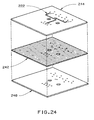
- a standard printed circuit board 224 is preferably constructed with a conductive lamina 242 disposed between connectors 228 and 230, closely adjacent to traces 222 of printed circuit board.
- Conductive lamina 242 can be formed of a layer of silver conductive ink or metal foil as described above.
- Fig. 24 discloses conductive lamina 242 disposed between a printed circuit board 244 that only has conductive traces 222 on its top surface and printed circuit board 246 that only has conductive traces (not shown) on its bottom surface, such that the insulating inner surfaces of printed circuit boards 244 and 246 act as a dielectric between conductive lamina 242 and traces 222.
- Figs 25 and 26 each disclose a printed circuit board 248 that has conductive traces on each side of board 248 which are spaced from conductive lamina 242 by an insulating layer 250.
- Insulating layer 250 is preferably constructed of a thin layer of Dupont's Kapton TM or similar material.
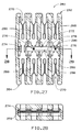
- FIG. 27 and 28 Another embodiment of the present invention, as seen in Figs. 27 and 28, includes a punch-down block connector 260 having an insulating plastic housing including upper and lower portions 262 and 264, insulation displacement contacts each having upper and lower metal insulation displacement contact portions 266 and 268 with each having insulation displacement slots 270 for terminating communication wires (not shown) a capacitor label strip 272 and a conductive lamina strip 274.
- Punch-down block 260 is constructed to terminate individual wires of twisted wire pairs of communication cables. Typically, each wire of a twisted pair is terminated to adjacent contacts.
- block 260 is illustrated having both upper and lower housing portions 262 and 264, a housing mounting a single row of contacts each of which includes a circuit board mounting post projecting from the housing for connection to a printed circuit board is also within the concept of the present invention.
- a capacitor label strip 272 and conductive lamina strip 274 are disposed closely adjacent to opposite sides of a medial portion of the contacts.
- Conductive lamina strip 274 preferably comprises a silver ink or a metal foil lamina respectively printed or adhesively secured between insulating layers.
- Capacitor label strip 272 can be constructed in a like manner to the capacitor labels described above to electrically and capacitively couple every other contact. Capacitor label strip 272 may be conductively attached to one, both or none of the coupled contacts in the manner described above, the preferred method conductively joining conductive laminas of label strip 272 to every other contact with liquid conductive adhesive.
- Twisted wire pairs can be terminated to adjacent contacts such that capacitively coupling every other contact capacitively couples a contact of one contact pair to a contact of a second contact pair.
- the contact conductive laminas of capacitor label strip 272 are positioned at zones 276 and are conductively attached to every other contact by conductive adhesive.
- Overlapping capacitor conductive laminas separated by a dielectric are positioned at a capacitor zone 278 and are connected to the contact conductive laminas at zones 276 by conductive traces positioned along dotted lines 280.
- Fig. 29 illustrates in more detail the construction of a capacitor label strip 290 which is one of the possible designs of capacitor label strip 272 of Figs. 26 and 27.
- Capacitor label strip 290 is used in the same manner and for the same purpose as capacitor label strip 272 of Figs. 27 and 28.
- Fig. 29 illustrates a portion of a capacitor label strip that is designed to capacitively couple every other contact of three pair of adjacent contacts. The portion of the strip of Fig. 29 may be repeated to provide a capacitor label strip that can capacitively couple any number of contact pairs.
- Strip 290 includes a Kapton TM insulating layer 292 upon which are printed a C1 conductive lamina 294 and a C5 conductive lamina 296; a printed dielectric lamina 298 having marginally disposed access notches 300; a C3 printed conductive lamina 302; and a printed insulating lamina 304 having marginally disposed access notches 306 and medially disposed access window 308.
- a layer of 3M's Scotch T "" 9703 anisotropic conductive adhesive transfer tape 310 is adhesively secured to insulating lamina 304 and, through aligned access notches 300 and 306 and access window 308, to C1, C3 and C5 conductive laminas 294, 302 and 296.
- Capacitor label strip 290 is aligned with and adhesively secured to the contacts of the contact row such that every other contact is aligned with a respective portion of conductive tape 310 that is in conductive contact with a respective one of conductive laminas 294, 302 and 296. Since tape 310 only conducts electricity through its thickness and not along the plane of the tape, every other contact is only conductively connected to a respective conductive lamina 294, 302 or 296 and thus every other contact is capacitively coupled to the next closest contact by overlapping portions of conductive laminas 294, 302 and 296.
- the preferred and alternative materials and construction methods for capacitor label strip 290 are the same as the materials and construction methods of the above described capacitor labels.
Landscapes
- Details Of Connecting Devices For Male And Female Coupling (AREA)
- Fixed Capacitors And Capacitor Manufacturing Machines (AREA)
Applications Claiming Priority (2)
| Application Number | Priority Date | Filing Date | Title |
|---|---|---|---|
| US08/997,277 US5513065A (en) | 1992-12-23 | 1992-12-23 | Communication connector with capacitor label |
| US997277 | 1997-12-23 |
Publications (3)
| Publication Number | Publication Date |
|---|---|
| EP0603667A2 true EP0603667A2 (fr) | 1994-06-29 |
| EP0603667A3 EP0603667A3 (fr) | 1996-01-24 |
| EP0603667B1 EP0603667B1 (fr) | 2002-02-27 |
Family
ID=25543826
Family Applications (1)
| Application Number | Title | Priority Date | Filing Date |
|---|---|---|---|
| EP93119879A Expired - Lifetime EP0603667B1 (fr) | 1992-12-23 | 1993-12-09 | Connecteur de communication avec condensateur multicouche |
Country Status (5)
| Country | Link |
|---|---|
| US (2) | US5513065A (fr) |
| EP (1) | EP0603667B1 (fr) |
| JP (1) | JPH06243937A (fr) |
| DE (1) | DE69331624D1 (fr) |
| TW (1) | TW218060B (fr) |
Cited By (10)
| Publication number | Priority date | Publication date | Assignee | Title |
|---|---|---|---|---|
| FR2729510A1 (fr) * | 1995-01-13 | 1996-07-19 | Arnould App Electr | Dispositif de raccordement electrique, en particulier pour reseau de telecommunication |
| EP0724338A2 (fr) * | 1995-01-27 | 1996-07-31 | Fluke Corporation | Appareil de mesure de diaphonie basés sur des impulsions avec compensation de diaphonie du connecteur |
| WO1997019499A1 (fr) * | 1995-11-17 | 1997-05-29 | The Whitaker Corporation | Jack modulaire a reduction amelioree de la diaphonie |
| EP0969569A2 (fr) * | 1998-06-05 | 2000-01-05 | Molex Incorporated | Correction de diaphonie pour connecteurs électriques |
| US6017247A (en) * | 1997-03-05 | 2000-01-25 | Krone Aktiengesellschaft | Arrangement of contact pairs for compensation of near-end crosstalk |
| EP0982815A2 (fr) * | 1998-08-24 | 2000-03-01 | Panduit Corporation | Connecteur modulaire avec interférences réduites |
| EP0993081A2 (fr) * | 1998-10-06 | 2000-04-12 | The Whitaker Corporation | Connecteur modulaire avec séparateurs capacitifs |
| EP1014513A2 (fr) * | 1998-12-17 | 2000-06-28 | Thomas & Betts International, Inc. | Circuit imprimé pour fiche modulaire |
| EP3134945A4 (fr) * | 2014-04-23 | 2017-11-01 | TE Connectivity Corporation | Connecteur électrique à capuchon de protection et à bornes protégées |
| DE112004000399B4 (de) | 2003-03-21 | 2019-03-28 | Commscope Solutions Properties, Llc | Endnahe Übersprechen-Kompensation bei Vielfach-Stufen |
Families Citing this family (76)
| Publication number | Priority date | Publication date | Assignee | Title |
|---|---|---|---|---|
| US6758698B1 (en) | 1992-12-23 | 2004-07-06 | Panduit Corp. | Communication connector with capacitor label |
| TW218060B (en) * | 1992-12-23 | 1993-12-21 | Panduit Corp | Communication connector with capacitor label |
| US6464529B1 (en) * | 1993-03-12 | 2002-10-15 | Cekan/Cdt A/S | Connector element for high-speed data communications |
| CA2178681C (fr) * | 1995-06-15 | 2001-01-16 | Attilio Joseph Rainal | Connecteur modulaire a faible niveau de diaphonie |
| GB9516804D0 (en) * | 1995-08-16 | 1995-10-18 | Amp Great Britain | Umbilical cord for projectile launching device |
| US5879199A (en) | 1996-02-29 | 1999-03-09 | Berg Technology, Inc. | Modular jack assembly and universal housing for use therein |
| US6739027B1 (en) * | 1996-06-12 | 2004-05-25 | International Business Machines Corporation | Method for producing printed circuit board with embedded decoupling capacitance |
| US6033263A (en) * | 1996-10-15 | 2000-03-07 | The Whitaker Corporation | Electrically connector with capacitive coupling |
| US5924896A (en) * | 1997-08-01 | 1999-07-20 | Lucent Technologies Inc. | High frequency communication jack |
| US5964600A (en) * | 1998-06-05 | 1999-10-12 | Molex Incorporated | Shuttered electrical connector |
| USRE38519E1 (en) * | 1998-08-24 | 2004-05-18 | Panduit Corp. | Low crosstalk modular communication connector |
| CA2291373C (fr) | 1998-12-02 | 2002-08-06 | Nordx/Cdt, Inc. | Connecteurs modulaires a structures de compensation |
| US6139368A (en) * | 1998-12-21 | 2000-10-31 | Thomas & Betts International, Inc. | Filtered modular connector |
| US6142831A (en) * | 1999-02-01 | 2000-11-07 | Aux Corporation | Multifunction connector assembly |
| US6290546B1 (en) * | 1999-02-02 | 2001-09-18 | Avaya Technology Corp. | Communication connector with signal compensation |
| AUPQ056099A0 (en) * | 1999-05-25 | 1999-06-17 | Silverbrook Research Pty Ltd | A method and apparatus (pprint01) |
| US6565385B1 (en) * | 1999-07-21 | 2003-05-20 | Cisco Technology, Inc. | Reducing electromagnetic emissions from a connector coupled to a printed circuit board |
| US6132260A (en) * | 1999-08-10 | 2000-10-17 | Hon Hai Precision Ind. Co., Ltd. | Modular connector assembly |
| US6089923A (en) | 1999-08-20 | 2000-07-18 | Adc Telecommunications, Inc. | Jack including crosstalk compensation for printed circuit board |
| US6325672B1 (en) | 1999-10-16 | 2001-12-04 | Berg Technology, Inc. | Electrical connector with internal shield and filter |
| US6390851B1 (en) | 1999-10-16 | 2002-05-21 | Berg Technology, Inc. | Electrical connector with internal shield |
| US6962503B2 (en) | 2000-01-10 | 2005-11-08 | Ortronics, Inc. | Unshielded twisted pair (UTP) wire stabilizer for communication plug |
| US6533618B1 (en) | 2000-03-31 | 2003-03-18 | Ortronics, Inc. | Bi-directional balance low noise communication interface |
| KR100372010B1 (ko) * | 2000-07-20 | 2003-02-14 | 이중근 | 인쇄기판회로 패턴을 이용한 인핸스드 카테고리 5급모듈라 잭 |
| US6729901B2 (en) | 2000-09-29 | 2004-05-04 | Ortronics, Inc. | Wire guide sled hardware for communication plug |
| US6802743B2 (en) * | 2000-09-29 | 2004-10-12 | Ortronics, Inc. | Low noise communication modular connector insert |
| US6843657B2 (en) * | 2001-01-12 | 2005-01-18 | Litton Systems Inc. | High speed, high density interconnect system for differential and single-ended transmission applications |
| US6979202B2 (en) * | 2001-01-12 | 2005-12-27 | Litton Systems, Inc. | High-speed electrical connector |
| US6554653B2 (en) | 2001-03-16 | 2003-04-29 | Adc Telecommunications, Inc. | Telecommunications connector with spring assembly and method for assembling |
| US6896557B2 (en) | 2001-03-28 | 2005-05-24 | Ortronics, Inc. | Dual reactance low noise modular connector insert |
| US7172466B2 (en) * | 2001-04-05 | 2007-02-06 | Ortronics, Inc. | Dual reactance low noise modular connector insert |
| DE10233318C1 (de) * | 2002-07-22 | 2003-09-25 | Siemens Ag | Entstöreinrichtung |
| US6641443B1 (en) | 2002-09-27 | 2003-11-04 | Leviton Manufacturing Co., Inc. | Electrical connector jack |
| US6786776B2 (en) * | 2002-09-27 | 2004-09-07 | Leviton Manufacturing Co., Inc. | Electrical connector jack |
| US7052328B2 (en) * | 2002-11-27 | 2006-05-30 | Panduit Corp. | Electronic connector and method of performing electronic connection |
| US6766793B2 (en) * | 2002-12-12 | 2004-07-27 | General Atomics | Electromagnetic gun and rotating pulse forming network |
| US6821142B1 (en) | 2003-03-04 | 2004-11-23 | Hubbell Incorporated | Electrical connector with crosstalk reduction and control |
| US7806523B2 (en) * | 2003-08-08 | 2010-10-05 | Seiko Epson Corporation | Liquid ejecting apparatus and liquid container holder thereof |
| JP2005212221A (ja) * | 2004-01-28 | 2005-08-11 | Seiko Epson Corp | 液体噴射装置 |
| US6991098B2 (en) * | 2004-01-21 | 2006-01-31 | Silverbrook Research Pty Ltd | Consumer tote for a roll of wallpaper |
| CN1930746B (zh) * | 2004-03-12 | 2010-12-22 | 泛达公司 | 减小电连接器中串扰的方法及装置 |
| CA2464834A1 (fr) * | 2004-04-19 | 2005-10-19 | Nordx/Cdt Inc. | Connecteur |
| US7947371B2 (en) * | 2004-11-05 | 2011-05-24 | E. I. Du Pont De Nemours And Company | Single-walled carbon nanotube composites |
| KR100644992B1 (ko) * | 2005-01-11 | 2006-11-10 | 대은전자 주식회사 | 고속통신용 누화 소거 패턴 및 이를 포함하는 모듈러 잭 |
| US7804756B2 (en) * | 2005-10-11 | 2010-09-28 | Zoran Corporation | DVD−R/RW and DVD+R/RW recorders |
| WO2007095533A1 (fr) * | 2006-02-13 | 2007-08-23 | Panduit Corp. | Connecteur a compensation de diaphonie |
| US7381098B2 (en) | 2006-04-11 | 2008-06-03 | Adc Telecommunications, Inc. | Telecommunications jack with crosstalk multi-zone crosstalk compensation and method for designing |
| US7402085B2 (en) * | 2006-04-11 | 2008-07-22 | Adc Gmbh | Telecommunications jack with crosstalk compensation provided on a multi-layer circuit board |
| US7530854B2 (en) * | 2006-06-15 | 2009-05-12 | Ortronics, Inc. | Low noise multiport connector |
| US7429178B2 (en) * | 2006-09-12 | 2008-09-30 | Samtec, Inc. | Modular jack with removable contact array |
| US7288001B1 (en) | 2006-09-20 | 2007-10-30 | Ortronics, Inc. | Electrically isolated shielded multiport connector assembly |
| EP2082458B1 (fr) * | 2006-10-13 | 2015-06-03 | Tyco Electronics Services GmbH | Matériel de connexion avec compensation de diaphonie inductive et capacitive à plusieurs étages |
| AU2007201107B2 (en) | 2007-03-14 | 2011-06-23 | Tyco Electronics Services Gmbh | Electrical Connector |
| AU2007201102B2 (en) * | 2007-03-14 | 2010-11-04 | Tyco Electronics Services Gmbh | Electrical Connector |
| AU2007201109B2 (en) | 2007-03-14 | 2010-11-04 | Tyco Electronics Services Gmbh | Electrical Connector |
| AU2007201114B2 (en) * | 2007-03-14 | 2011-04-07 | Tyco Electronics Services Gmbh | Electrical Connector |
| AU2007201105B2 (en) | 2007-03-14 | 2011-08-04 | Tyco Electronics Services Gmbh | Electrical Connector |
| AU2007201108B2 (en) * | 2007-03-14 | 2012-02-09 | Tyco Electronics Services Gmbh | Electrical Connector |
| AU2007201106B9 (en) * | 2007-03-14 | 2011-06-02 | Tyco Electronics Services Gmbh | Electrical Connector |
| AU2007201113B2 (en) * | 2007-03-14 | 2011-09-08 | Tyco Electronics Services Gmbh | Electrical Connector |
| US7485010B2 (en) * | 2007-06-14 | 2009-02-03 | Ortronics, Inc. | Modular connector exhibiting quad reactance balance functionality |
| US7481678B2 (en) * | 2007-06-14 | 2009-01-27 | Ortronics, Inc. | Modular insert and jack including bi-sectional lead frames |
| US7967645B2 (en) * | 2007-09-19 | 2011-06-28 | Leviton Manufacturing Co., Inc. | High speed data communications connector circuits, systems, and methods for reducing crosstalk in communications systems |
| US7841909B2 (en) | 2008-02-12 | 2010-11-30 | Adc Gmbh | Multistage capacitive far end crosstalk compensation arrangement |
| USD612856S1 (en) | 2008-02-20 | 2010-03-30 | Vocollect Healthcare Systems, Inc. | Connector for a peripheral device |
| US7976348B2 (en) * | 2008-05-07 | 2011-07-12 | Ortronics, Inc. | Modular insert and jack including moveable reactance section |
| US7601034B1 (en) | 2008-05-07 | 2009-10-13 | Ortronics, Inc. | Modular insert and jack including moveable reactance section |
| MX2011001542A (es) * | 2008-08-13 | 2011-03-30 | Panduit Corp | Conector de comunicaciones con compensacion de etapas multiples. |
| KR101604629B1 (ko) * | 2008-08-20 | 2016-03-18 | 팬듀트 코포레이션 | 다단계 보상을 갖는 고속 커넥터 |
| EP2209172A1 (fr) | 2009-01-15 | 2010-07-21 | 3M Innovative Properties Company | Connecteur de télécommunications doté d'une carte à circuit imprimé multicouche |
| USD615040S1 (en) | 2009-09-09 | 2010-05-04 | Vocollect, Inc. | Electrical connector |
| US8262403B2 (en) * | 2009-09-10 | 2012-09-11 | Vocollect, Inc. | Break-away electrical connector |
| US8241053B2 (en) * | 2009-09-10 | 2012-08-14 | Vocollect, Inc. | Electrical cable with strength member |
| US7850492B1 (en) | 2009-11-03 | 2010-12-14 | Panduit Corp. | Communication connector with improved crosstalk compensation |
| WO2016099484A1 (fr) * | 2014-12-17 | 2016-06-23 | Hewlett Packard Enterprise Development Lp | Dispositif de désactivation comportant un adhésif pour désactiver une interface électrique |
| WO2017042373A1 (fr) * | 2015-09-10 | 2017-03-16 | Te Connectivity Germany Gmbh | Agencement de contact et procédé de réduction de diaphonie |
Citations (5)
| Publication number | Priority date | Publication date | Assignee | Title |
|---|---|---|---|---|
| US4418239A (en) * | 1981-08-24 | 1983-11-29 | Oak Industries Inc. | Flexible connector with interconnection between conductive traces |
| JPS6486795A (en) * | 1987-09-29 | 1989-03-31 | Toshiba Corp | Capacitive coupling cancelation circuit between adjacent voice signal paths |
| DE4103321A1 (de) * | 1990-02-03 | 1991-08-08 | Murata Manufacturing Co | Verbinder |
| WO1994005092A1 (fr) * | 1992-08-24 | 1994-03-03 | British Telecommunications Public Limited Company | Dispositif et procede de suppression de diaphonie dans des correcteurs de donnees |
| US5295869A (en) * | 1992-12-18 | 1994-03-22 | The Siemon Company | Electrically balanced connector assembly |
Family Cites Families (30)
| Publication number | Priority date | Publication date | Assignee | Title |
|---|---|---|---|---|
| US3098955A (en) * | 1959-07-31 | 1963-07-23 | Benjamin L Davis | Tape capacitor |
| US3743978A (en) * | 1969-12-09 | 1973-07-03 | W Fritz | Coated ferrite rf filters |
| US4342143A (en) * | 1974-02-04 | 1982-08-03 | Jennings Thomas A | Method of making multiple electrical components in integrated microminiature form |
| US4126840A (en) * | 1977-03-14 | 1978-11-21 | International Telephone And Telegraph Corporation | Filter connector |
| JPS57168540A (en) * | 1981-04-10 | 1982-10-16 | Nissan Motor Co Ltd | Noise preventing device and its production for electronic controller |
| US4726638A (en) * | 1985-07-26 | 1988-02-23 | Amp Incorporated | Transient suppression assembly |
| US4654749A (en) * | 1985-07-30 | 1987-03-31 | Murata Manufacturing Co., Ltd. | High-voltage ceramic capacitor and method of producing the same |
| US4678251A (en) * | 1986-02-10 | 1987-07-07 | Installation Technology, Inc. | Modular installation system for data cable interfacing |
| CH677988A5 (fr) * | 1986-07-30 | 1991-07-15 | Actron Entwicklungs Ag | |
| US4695115A (en) * | 1986-08-29 | 1987-09-22 | Corcom, Inc. | Telephone connector with bypass capacitor |
| NL8701661A (nl) * | 1987-07-14 | 1989-02-01 | Du Pont Nederland | Filtereenheid voor connectoren. |
| US4772224A (en) * | 1987-09-02 | 1988-09-20 | Corcom, Inc. | Modular electrical connector |
| GB2212006B (en) * | 1987-11-05 | 1991-11-20 | British Telecomm | Improvements in or relating to line verification testing |
| US4799901A (en) * | 1988-06-30 | 1989-01-24 | Pirc Douglas J | Adapter having transient suppression protection |
| JPH07120542B2 (ja) * | 1988-12-12 | 1995-12-20 | 株式会社村田製作所 | モジュラージャック |
| JPH02162667A (ja) * | 1988-12-15 | 1990-06-22 | Oki Densen Kk | モールド基板形モジュラージャック |
| JP2655430B2 (ja) * | 1989-03-10 | 1997-09-17 | 日本電気株式会社 | 同軸―マイクロストリップ線路変換器 |
| JP2833049B2 (ja) * | 1989-09-27 | 1998-12-09 | 松下電器産業株式会社 | プリント配線板 |
| US5006822A (en) * | 1990-01-03 | 1991-04-09 | Prabhakara Reddy | Hybrid RF coupling device with integrated capacitors and resistors |
| US5178554A (en) * | 1990-10-26 | 1993-01-12 | The Siemon Company | Modular jack patching device |
| US5139442A (en) * | 1990-12-03 | 1992-08-18 | Murata Manufacturing Co., Ltd. | Modular jack |
| US5118310A (en) * | 1991-03-06 | 1992-06-02 | Panduit Corp. | Central latch modular telephone connector |
| US5282759A (en) * | 1991-09-13 | 1994-02-01 | Murata Manufacturing Co., Ltd. | Modular jack |
| US5205762A (en) * | 1991-12-06 | 1993-04-27 | Porta Systems Corp. | High frequency patch cord data connector |
| US5186647A (en) * | 1992-02-24 | 1993-02-16 | At&T Bell Laboratories | High frequency electrical connector |
| US5299956B1 (en) * | 1992-03-23 | 1995-10-24 | Superior Modular Prod Inc | Low cross talk electrical connector system |
| CA2072380C (fr) * | 1992-06-25 | 2000-08-01 | Michel Bohbot | Modules de circuits faits de cartes de circuits imprimes et de connecteurs de telecommunication |
| US5269705A (en) * | 1992-11-03 | 1993-12-14 | The Whitaker Corporation | Tape filter and method of applying same to an electrical connector |
| TW218060B (en) * | 1992-12-23 | 1993-12-21 | Panduit Corp | Communication connector with capacitor label |
| US5470244A (en) * | 1993-10-05 | 1995-11-28 | Thomas & Betts Corporation | Electrical connector having reduced cross-talk |
-
1992
- 1992-12-16 TW TW081110095A patent/TW218060B/zh active
- 1992-12-23 US US08/997,277 patent/US5513065A/en not_active Expired - Lifetime
-
1993
- 1993-12-09 EP EP93119879A patent/EP0603667B1/fr not_active Expired - Lifetime
- 1993-12-09 DE DE69331624T patent/DE69331624D1/de not_active Expired - Lifetime
- 1993-12-24 JP JP5328313A patent/JPH06243937A/ja active Pending
-
1996
- 1996-04-26 US US08/639,883 patent/US5940959A/en not_active Expired - Fee Related
Patent Citations (5)
| Publication number | Priority date | Publication date | Assignee | Title |
|---|---|---|---|---|
| US4418239A (en) * | 1981-08-24 | 1983-11-29 | Oak Industries Inc. | Flexible connector with interconnection between conductive traces |
| JPS6486795A (en) * | 1987-09-29 | 1989-03-31 | Toshiba Corp | Capacitive coupling cancelation circuit between adjacent voice signal paths |
| DE4103321A1 (de) * | 1990-02-03 | 1991-08-08 | Murata Manufacturing Co | Verbinder |
| WO1994005092A1 (fr) * | 1992-08-24 | 1994-03-03 | British Telecommunications Public Limited Company | Dispositif et procede de suppression de diaphonie dans des correcteurs de donnees |
| US5295869A (en) * | 1992-12-18 | 1994-03-22 | The Siemon Company | Electrically balanced connector assembly |
Non-Patent Citations (1)
| Title |
|---|
| PATENT ABSTRACTS OF JAPAN vol. 013 no. 321 (E-790) ,20 July 1989 & JP-A-01 086795 (TOSHIBA CORP) 31 March 1989, * |
Cited By (19)
| Publication number | Priority date | Publication date | Assignee | Title |
|---|---|---|---|---|
| FR2729510A1 (fr) * | 1995-01-13 | 1996-07-19 | Arnould App Electr | Dispositif de raccordement electrique, en particulier pour reseau de telecommunication |
| EP0724338A2 (fr) * | 1995-01-27 | 1996-07-31 | Fluke Corporation | Appareil de mesure de diaphonie basés sur des impulsions avec compensation de diaphonie du connecteur |
| EP0724338A3 (fr) * | 1995-01-27 | 1996-08-28 | Fluke Corp | |
| WO1997019499A1 (fr) * | 1995-11-17 | 1997-05-29 | The Whitaker Corporation | Jack modulaire a reduction amelioree de la diaphonie |
| US6017247A (en) * | 1997-03-05 | 2000-01-25 | Krone Aktiengesellschaft | Arrangement of contact pairs for compensation of near-end crosstalk |
| EP0969569A3 (fr) * | 1998-06-05 | 2000-05-24 | Molex Incorporated | Correction de diaphonie pour connecteurs électriques |
| AU751906B2 (en) * | 1998-06-05 | 2002-08-29 | Molex Incorporated | Crosstalk correction in electrical connectors |
| EP0969569A2 (fr) * | 1998-06-05 | 2000-01-05 | Molex Incorporated | Correction de diaphonie pour connecteurs électriques |
| EP0982815A2 (fr) * | 1998-08-24 | 2000-03-01 | Panduit Corporation | Connecteur modulaire avec interférences réduites |
| EP1622234A1 (fr) | 1998-08-24 | 2006-02-01 | Panduit Corporation | Connecteur de communication modulaire à faible diaphonie |
| EP0982815A3 (fr) * | 1998-08-24 | 2001-06-20 | Panduit Corporation | Connecteur modulaire avec interférences réduites |
| EP0993081A2 (fr) * | 1998-10-06 | 2000-04-12 | The Whitaker Corporation | Connecteur modulaire avec séparateurs capacitifs |
| EP0993081A3 (fr) * | 1998-10-06 | 2001-12-19 | The Whitaker Corporation | Connecteur modulaire avec séparateurs capacitifs |
| EP1014513A2 (fr) * | 1998-12-17 | 2000-06-28 | Thomas & Betts International, Inc. | Circuit imprimé pour fiche modulaire |
| EP1014513A3 (fr) * | 1998-12-17 | 2000-11-08 | Thomas & Betts International, Inc. | Circuit imprimé pour fiche modulaire |
| DE112004000399B4 (de) | 2003-03-21 | 2019-03-28 | Commscope Solutions Properties, Llc | Endnahe Übersprechen-Kompensation bei Vielfach-Stufen |
| EP3134945A4 (fr) * | 2014-04-23 | 2017-11-01 | TE Connectivity Corporation | Connecteur électrique à capuchon de protection et à bornes protégées |
| US9847607B2 (en) | 2014-04-23 | 2017-12-19 | Commscope Technologies Llc | Electrical connector with shield cap and shielded terminals |
| US10476212B2 (en) | 2014-04-23 | 2019-11-12 | Commscope Technologies Llc | Electrical connector with shield cap and shielded terminals |
Also Published As
| Publication number | Publication date |
|---|---|
| TW218060B (en) | 1993-12-21 |
| JPH06243937A (ja) | 1994-09-02 |
| EP0603667B1 (fr) | 2002-02-27 |
| US5513065A (en) | 1996-04-30 |
| US5940959A (en) | 1999-08-24 |
| DE69331624D1 (de) | 2002-04-04 |
| EP0603667A3 (fr) | 1996-01-24 |
Similar Documents
| Publication | Publication Date | Title |
|---|---|---|
| EP0603667B1 (fr) | Connecteur de communication avec condensateur multicouche | |
| US4714435A (en) | Connection for flexible apparatus | |
| US4389080A (en) | Plug-in ceramic hybrid module | |
| US5041015A (en) | Electrical jumper assembly | |
| US5244395A (en) | Circuit interconnect system | |
| US5414220A (en) | Flexible wiring cable | |
| US6758698B1 (en) | Communication connector with capacitor label | |
| EP0490530A2 (fr) | Circuit imprimé flexible | |
| US20020157865A1 (en) | Flexible flat circuitry with improved shielding | |
| CA2464834A1 (fr) | Connecteur | |
| US5277625A (en) | Electrical connector with tape filter | |
| US4599486A (en) | High capacitance bus bar including multilayer ceramic capacitors | |
| US5269705A (en) | Tape filter and method of applying same to an electrical connector | |
| US6608258B1 (en) | High data rate coaxial interconnect technology between printed wiring boards | |
| US20020125967A1 (en) | Air dielectric backplane interconnection system | |
| EP0226276B1 (fr) | Assemblage pour la connexion électrique entre un circuit flexible et un autre circuit | |
| EP0393251B1 (fr) | Système connexion modulaire, avec connecteurs montés en surface à haute densité des éléments de contact | |
| EP0645849B1 (fr) | Connecteur ayant des filtres | |
| CA2120326C (fr) | Structure de dispositif electrotechnique | |
| EP0596216B1 (fr) | Filtre à ruban et procédé d'application à un connecteur électrique | |
| CN109890134B (zh) | 一种柔性电路板 | |
| US5364293A (en) | Shielded stackable solderless connector/filter assembly | |
| WO1996009748A1 (fr) | Reseau de cables plan | |
| JPH0750499A (ja) | フレキシブル印刷配線板のシールド装置 | |
| KR0155365B1 (ko) | 높은 접촉 요소 밀도로 표면 장착된 커넥터를 구비한 모듈 커넥터 시스템 |
Legal Events
| Date | Code | Title | Description |
|---|---|---|---|
| PUAI | Public reference made under article 153(3) epc to a published international application that has entered the european phase |
Free format text: ORIGINAL CODE: 0009012 |
|
| AK | Designated contracting states |
Kind code of ref document: A2 Designated state(s): DE FR GB IT |
|
| PUAL | Search report despatched |
Free format text: ORIGINAL CODE: 0009013 |
|
| AK | Designated contracting states |
Kind code of ref document: A3 Designated state(s): DE FR GB IT |
|
| 17P | Request for examination filed |
Effective date: 19960724 |
|
| 17Q | First examination report despatched |
Effective date: 19971222 |
|
| GRAG | Despatch of communication of intention to grant |
Free format text: ORIGINAL CODE: EPIDOS AGRA |
|
| GRAG | Despatch of communication of intention to grant |
Free format text: ORIGINAL CODE: EPIDOS AGRA |
|
| GRAG | Despatch of communication of intention to grant |
Free format text: ORIGINAL CODE: EPIDOS AGRA |
|
| GRAH | Despatch of communication of intention to grant a patent |
Free format text: ORIGINAL CODE: EPIDOS IGRA |
|
| GRAH | Despatch of communication of intention to grant a patent |
Free format text: ORIGINAL CODE: EPIDOS IGRA |
|
| RIC1 | Information provided on ipc code assigned before grant |
Free format text: 7H 01R 13/719 A, 7H 01R 13/66 B, 7H 01R 24/04 B |
|
| REG | Reference to a national code |
Ref country code: GB Ref legal event code: IF02 |
|
| GRAA | (expected) grant |
Free format text: ORIGINAL CODE: 0009210 |
|
| AK | Designated contracting states |
Kind code of ref document: B1 Designated state(s): DE FR GB IT |
|
| PG25 | Lapsed in a contracting state [announced via postgrant information from national office to epo] |
Ref country code: IT Free format text: LAPSE BECAUSE OF FAILURE TO SUBMIT A TRANSLATION OF THE DESCRIPTION OR TO PAY THE FEE WITHIN THE PRE;WARNING: LAPSES OF ITALIAN PATENTS WITH EFFECTIVE DATE BEFORE 2007 MAY HAVE OCCURRED AT ANY TIME BEFORE 2007. THE CORRECT EFFECTIVE DATE MAY BE DIFFERENT FROM THE ONE RECORDED.SCRIBED TIME-LIMIT Effective date: 20020227 Ref country code: FR Free format text: LAPSE BECAUSE OF FAILURE TO SUBMIT A TRANSLATION OF THE DESCRIPTION OR TO PAY THE FEE WITHIN THE PRESCRIBED TIME-LIMIT Effective date: 20020227 |
|
| REF | Corresponds to: |
Ref document number: 69331624 Country of ref document: DE Date of ref document: 20020404 |
|
| PG25 | Lapsed in a contracting state [announced via postgrant information from national office to epo] |
Ref country code: DE Free format text: LAPSE BECAUSE OF FAILURE TO SUBMIT A TRANSLATION OF THE DESCRIPTION OR TO PAY THE FEE WITHIN THE PRESCRIBED TIME-LIMIT Effective date: 20020528 |
|
| EN | Fr: translation not filed | ||
| PLBE | No opposition filed within time limit |
Free format text: ORIGINAL CODE: 0009261 |
|
| STAA | Information on the status of an ep patent application or granted ep patent |
Free format text: STATUS: NO OPPOSITION FILED WITHIN TIME LIMIT |
|
| 26N | No opposition filed |
Effective date: 20021128 |
|
| PGFP | Annual fee paid to national office [announced via postgrant information from national office to epo] |
Ref country code: GB Payment date: 20091209 Year of fee payment: 17 |
|
| GBPC | Gb: european patent ceased through non-payment of renewal fee |
Effective date: 20101209 |
|
| PG25 | Lapsed in a contracting state [announced via postgrant information from national office to epo] |
Ref country code: GB Free format text: LAPSE BECAUSE OF NON-PAYMENT OF DUE FEES Effective date: 20101209 |