EP0601817A1 - Circuit de multiplication de la puissance - Google Patents
Circuit de multiplication de la puissance Download PDFInfo
- Publication number
- EP0601817A1 EP0601817A1 EP93309774A EP93309774A EP0601817A1 EP 0601817 A1 EP0601817 A1 EP 0601817A1 EP 93309774 A EP93309774 A EP 93309774A EP 93309774 A EP93309774 A EP 93309774A EP 0601817 A1 EP0601817 A1 EP 0601817A1
- Authority
- EP
- European Patent Office
- Prior art keywords
- voltage
- output voltage
- output
- terminal
- switch
- Prior art date
- Legal status (The legal status is an assumption and is not a legal conclusion. Google has not performed a legal analysis and makes no representation as to the accuracy of the status listed.)
- Granted
Links
Images


Classifications
-
- G—PHYSICS
- G01—MEASURING; TESTING
- G01R—MEASURING ELECTRIC VARIABLES; MEASURING MAGNETIC VARIABLES
- G01R11/00—Electromechanical arrangements for measuring time integral of electric power or current, e.g. of consumption
-
- G—PHYSICS
- G01—MEASURING; TESTING
- G01R—MEASURING ELECTRIC VARIABLES; MEASURING MAGNETIC VARIABLES
- G01R21/00—Arrangements for measuring electric power or power factor
- G01R21/08—Arrangements for measuring electric power or power factor by using galvanomagnetic-effect devices, e.g. Hall-effect devices
Definitions
- This invention relates to a power multiplication circuit using a Hall element, and more particularly to a power multiplication circuit used in, such as a power meter or a watt hour meter, wherein the offset compensation means of the Hall element is improved.
- power multiplication circuits of this type are widely used as power multiplication circuits of power meters and/or watt hour meters on account of their uncomplicated construction and small size.
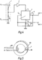
- a conventional power multiplication circuit will now be described with reference to Fig. 4.
- the power source voltage of a system under measurement is input at input terminals P1, P2, passes through a voltage conversion circuit 1 comprising a voltage divider circuit with resistors RA and RB, and is input to a voltage-current conversion circuit 2.
- Voltage-current conversion circuit 2 outputs a current proportional to the input voltage to control current terminal T1 of Hall element 3.
- the current from the system under measurement is input to terminals 1S, 1L of current coil 105 wound on magnetic material core 104 shown in Fig.
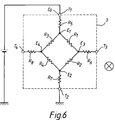
- the equivalent circuit is expressed by a resistance bridge circuit, as shown.
- the output voltage is given by expression (2), if the respective voltages at the nodes are taken as E1, E2, E3, and E4 when the voltage E0 is applied to terminal T1 and the bridge resistances are respectively R1, R2, R3 and R4.
- the voltage E0 and resistances R5, T6, R7 and R8 are not expressed positively, they are included in the voltages E1, E2, E3 and E4, and when Hall element 3 is connected to a following circuit having a very high input impedance, the output voltage between terminals T3 and T4 of Hall element 3 is nearly equal to the voltage (E3 - E4) expressed in the expression (2).
- E3-E4 R2 ⁇ R3 - (R1-r1)R4 (R1-r1+R2)(R3+R4) (E1-E2) ⁇ 0
- the lower row indicates the waveform of the output voltage which is shown by broken lines in the case where there is no offset. If now we assume that the offset of resistor R1 is generated in the direction of decreasing resistance, the output voltage is decreased or increased by the amount of the offset voltage, as shown by the continuous line in the bottom row of Fig. 7. Accordingly, the output voltage is adjusted to zero in the condition where magnetic field is not applied by providing a variable resistor VR1 as shown in Fig. 4 to cancel the deviation of the output voltage produced by this offset voltage.
- one objection of this invention is to provide a power multiplication circuit wherein fluctuation in the offset voltage due to temperature change or change over a period of years etc. can be automatically corrected.
- a power multiplication circuit comprising: a Hall element for generating between voltage output terminals thereof a first output voltage corresponding to power of a system under measurement; operating means connected to receive said first output voltage for amplifying said first output voltage and for changing over between amplified first output voltage and an inverted amplified first output voltage in alternate time periods corresponding to the length of a half cycle of said system under measurement to generate a second output voltage; integrating means for integrating said second output voltage to generate an integrated signal; and a variable resistance member connected between one of said voltage output terminals of said Hall element member and ground, and connected to receive said integrated signal, the resistance thereof being controlled by said integrated signal so as to compensate offset voltage of said Hall element member.
- a power meter for detecting a power of a system.
- the power meter includes a voltage-current conversion circuit connected to receive a power source voltage of the system under measurement for converting the power source voltage to a control current proportional to the power source voltage and a Hall element.
- the Hall element is provided with control current input terminals and voltage output terminals and is positioned in a magnetic field such that a plane thereof created by the control current input terminals and the voltage output terminals is substantially perpendicular to the magnetic field.
- An intensity of the magnetic field is proportional to a current of the system under measurement.
- the Hall element is connected to the voltage-current conversion circuit such that the control current flows through the control current input terminals and generates a first output voltage corresponding to the power of said system under measurement between the voltage output terminals.
- the power meter further includes a voltage polarity detection circuit for detecting a polarity of the power source voltage of the system under measurement and an operating amplifier circuit connected to receive the first output voltage and for amplifying the first output voltage to generate amplified first output voltage and an inverted voltage of the amplified first output voltage.
- An output terminal of the power meter is connected to the operating amplifier circuit for outputting the amplified first output voltage as the power of the system under measurement.
- the power meter also includes a switch circuit connected to receive the amplified first output voltage, the inverted voltage and the polarity for changing over the amplified first output voltage and the inverted voltage to generate a second output voltage in accordance with the polarity and an integrating amplifier for integrating the second output voltage to generate an integrated signal.
- the power meter further includes a variable resistance element connected between one of the voltage output terminals of the Hall element and ground and connected to receive the integrated signal. A resistance thereof is changed by the integrated signal so that an offset voltage of the Hall element is reduced to zero.
- the integrated value of the offset voltage is increased or decreased, with directionality, by arranging for the input to the integration circuit to be changed over in response to the polarity of the power source voltage of the system under measurement.
- the resistance of the variable resistor is thereby increased or decreased in response to the magnitude of the integrated value that is output by the integration circuit. This enables fluctuation of the offset resistance to be compensated such that the power can be calculated without offset.
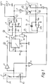
- Fig. 1 is a circuit diagram of a power multiplication circuit according to an embodiment of this invention.
- P1 and P2 are power source voltage input terminals that input the power source voltage, such as a.c. 100 volts of the system under measurement.
- a voltage conversion circuit 1 converts the power source voltage input to input terminals P1 and P2 to a voltage suitable for matching the voltage in the power multiplication circuit by stepping up or stepping down.
- This voltage conversion circuit 1 can be constituted using a voltage division circuit based on resistors RA, RB as shown in Fig. 1, or a transformer etc.
- a voltage-current conversion circuit 2 outputs a current proportional to the output voltage of voltage conversion circuit 1 at output terminal la.
- a Hall element 3 is provided with control current input terminals T1, T2 that input the current output from voltage-current conversion circuit 2, and with voltage output terminals T3, T4 that output the voltage obtained by the Hall effect.
- the construction is such that Hall element 3 is held in gap 106 of magnetic material core 104 around which current coil 105 is wound as shown in Fig. 5, and the-plane- containing control current input terminals T1, T2 and voltage output terminals T3, T4 is perpendicular to the magnetic field generated in the gap 106.
- the direction of the magnetic field is shown as an arrow x in Fig. 1.
- a subtracting amplifier 4 receives the AC voltages that are output at voltage output terminals T3, T4 of Hall element 3, and outputs the difference of the AC voltage to output terminal OUT1 of the power multification circuit. Output terminal OUT2 thereof is connected to ground.
- a sign inverting amplifier 5 inverts the polarity of the voltage applied from subtracting amplifier 4.
- a voltage polarity detection circuit 6 is connected between input terminal P2 and output terminal la of voltage conversion circuit 1 that ascertains the polarity of the power source voltage of the system that is the subject of measurement.
- the output of voltage polarity detection circuit 6 is used such that if the ascertained polarity is positive a switch SW1 is closed and a switch SW2 is opened through an inverter 8, and if the ascertained polarity is negative switch SW1 is opened and switch SW2 is closed through inverter 8.
- Switches SW1 and SW2 in a switch circuit 7 are respectively switches that are put in the closed condition by an input signal of level "1" and put in the open condition by an input signal of level "0".
- the primary side of switch SW1 is connected to the output of sign inverting amplifier 5, while the primary side of switch SW2 is connected to the output of subtracting amplifier 4.
- An integrating amplifier 9 integrates the voltage output from the secondary side of switches SW1, SW2.
- a variable resistance element 10 is connected between ground and voltage output terminal T3, so that its resistance value is controlled by the output of integrating amplifier 9. It may be implemented using an FET or Cds photocoupler etc.
- Rc is a resistor connected between voltage output terminal T4 and ground and is provided to take account of the case where the offset resistance r1 is negative.
- Subtracting amplifier 4 is constructed, for example, by an operational amplifier OP1 and resistors Rd, Re, Rf and Rg.
- Integrating amplifier 9 is constructed, for example, by an operational amplifier OP2, a resistor Rh and a capacitor Ca.
- the power source voltage of the system under measurement that is input to power source voltage input terminals P1, P2 is converted to the suitable voltage by voltage conversion circuit 1, which is input to voltage-current conversion circuit 2.
- the current obtained by converting the input voltage to a current proportional to it in voltage-current conversion circuit 2 flows into Hall element 3 from the control current input terminal T1 to terminal T2 of Hall element 3.
- the current of the system under measurement is made to flow to current coil 105 of magnetic material core 104, producing a magnetic field in gap 106 the intensity of which is proportional to the current of the system under measurement. This therefore results in the generation of a Hall electromotive force given by expression (1) at voltage output terminals T3, T4 of Hall element 3.
- the output voltage difference across voltage output terminals T3, T4 is therefore proportional to the product of the voltage and the current of the system under measurement. In other words, it is proportional to the power of the system under measurement.
- Subtracting amplifier 4 differentially amplifies its two inputs from voltage output terminals T3, T4 so that the output voltage difference across these voltage output terminals T3, T4 is output to the outside from output terminals OUT1 and OUT2 as the power value of the system under measurement.
- the switch circuit 7 is used to change the input to integrating amplifier 9, between the output of amplifier 4 and the inverted output of amplifier 4 provided by inverter 5, in alternate time periods corresponding to the length of a half cycle of the power supply.
- the polarity of the power source voltage of the system under measurement which has been subjected to voltage conversion in voltage conversion circuit 1, is ascertained by voltage polarity detection circuit 6.
- the ascertained polarity is used by switch circuit 7 to change over the phase of the output voltage of subtracting amplifier 4 which is input to integrating amplifier 9.
- the operation is such that, for example, if the polarity of the power source voltage of the system under measurement is positive, switch SW1 is closed and switch SW2 is opened, so that an output voltage of sign inverting amplifier 5 in which the polarity of output voltage of subtracting amplifier 4 is inverted is input to integrating amplifier 9.
- variable resistance element 10 changes its resistance in the direction such as to compensate for the offset voltage, this change being made in accordance with the sign and the magnitude of the input voltage.
- the polarity of the current may be used to change between the inverted and non-inverted outputs of amplifier 4.
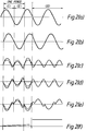
- FIG. 2 The magnetic field intensity in gap 106 of magnetic material core 104 is shown at (a).
- the current waveform of the output from voltage-current conversion circuit 2 that is input to Hall element 3 is shown at (b).
- the waveform of the output of subtracting amplifier 4 is shown at (c).
- the waveform when there is no offset is shown by a broken line, while the waveform when offset is present is shown by a continuous line. All of these waveforms are generated in accordance with the rules of combination of direction of magnetic field and polarity of the current shown in Fig. 7.
- the output waveform of sign inverting amplifier 5 is shown at (d) and is arrived at by inverting the waveform of (c).
- the waveform of the output of switch circuit 7 is shown at (e) and is obtained by operating switch circuit 7 by means of voltage polarity detection circuit 6 in response to the power source voltage of the system under measurement; it is also the waveform of the input to integrating amplifier 9.
- the output voltage of sign inverting amplifier 5 shown in (d) is input to integrating amplifier 9 by the closure of switch SW1.
- the output voltage of subtracting amplifier 4 shown in (c) is input to integrating amplifier 9 by the closure of switch SW2.
- the waveform expressed by a broken line in (e) in period (I) has the opposite polarity but equal magnitude to the waveform expressed by a broken line in (e) in period (II), so the output of integrating amplifier 9 is zero when integrated over one period including the period (I) and the period (II).
- the offset resistance r1 (r1 > 0) is present in Hall element 3 since the waveform, shown by the continuous line in (e), is offset in the negative direction, the output integrated by integrating amplifier 9, as shown in (f), is not zero.
- Variable resistance element 10 is controlled based on the output of the integrating amplifier 9 as follows.
- variable resistance element 10 decreases as the output voltage of integrating amplifier 9 increases, until it reaches a resistance that compensates the offset resistance r1 of Hall element 3.
- the input voltage waveform of integrating amplifier 9 then has a waveform as shown by the broken line in (e).
- the output of integrating amplifier 9, does not further change, and the resistance of variable resistance element 10 is then maintained unaltered in this condition, in the state of period (III).
- Resistor Rc is required to effect compensation in the case where offset resistance r1 is negative.
- the offset voltage generated by change in the characteristic of Hall element 3 can be automatically corrected, so that the power can be calculated accurately.
- Fig. 3 is a circuit diagram showing a power multification circuit according to another embodiment of this invention.
- the same benefits as in the first embodiment can be obtained by employing two amplifiers 12, 13 differing in phase by 180 degrees but of mutually equal gain in place of subtracting amplifier 4, by connecting operational amplifier 11 to voltage output terminal T4 of Hall element 3, and holding voltage output terminal T4 at ground level.
- inverter 8 is used for controlling switch SW2. But this invention is not limited to these embodiments.
- switch SW2 is a switch that is put in the open condition by an input signal of level "1" and put in the closed condition by an input signal of level "0"
- inverter 8 can be omitted and switch SW2 is controlled directly by the output of voltage polarity detection circuit 6.
- switch circuit 7 is expressed by a circuit having a mechanical contact, a contact-less switch, such as a semiconductor switch, could of course be used.
- a power multiplication circuit can be provided which is of high accuracy and wherein fluctuations of the offset voltage produced by temperature change and change over a period of years can be automatically corrected.
Applications Claiming Priority (3)
| Application Number | Priority Date | Filing Date | Title |
|---|---|---|---|
| JP33084492 | 1992-12-11 | ||
| JP330844/92 | 1992-12-11 | ||
| JP4330844A JP3011559B2 (ja) | 1992-12-11 | 1992-12-11 | 電力乗算回路 |
Publications (2)
| Publication Number | Publication Date |
|---|---|
| EP0601817A1 true EP0601817A1 (fr) | 1994-06-15 |
| EP0601817B1 EP0601817B1 (fr) | 2004-11-17 |
Family
ID=18237171
Family Applications (1)
| Application Number | Title | Priority Date | Filing Date |
|---|---|---|---|
| EP93309774A Expired - Lifetime EP0601817B1 (fr) | 1992-12-11 | 1993-12-06 | Circuit de calculation de la puissance |
Country Status (5)
| Country | Link |
|---|---|
| US (1) | US5438258A (fr) |
| EP (1) | EP0601817B1 (fr) |
| JP (1) | JP3011559B2 (fr) |
| KR (1) | KR0125595B1 (fr) |
| DE (1) | DE69333695T2 (fr) |
Cited By (2)
| Publication number | Priority date | Publication date | Assignee | Title |
|---|---|---|---|---|
| EP0635726A2 (fr) * | 1993-07-21 | 1995-01-25 | Kabushiki Kaisha Toshiba | Dispositif pour le calcul d'une puissance |
| WO1996028739A1 (fr) * | 1995-03-16 | 1996-09-19 | Horstmann Timers & Controls Limited | Appareil de mesure d'electricite |
Families Citing this family (10)
| Publication number | Priority date | Publication date | Assignee | Title |
|---|---|---|---|---|
| JPH11352157A (ja) * | 1998-06-11 | 1999-12-24 | Yazaki Corp | 電源電圧検出方法及びその装置 |
| US6392400B1 (en) * | 1998-10-08 | 2002-05-21 | Schlumberger Resource Management Services | High linearity, low offset interface for Hall effect devices |
| US6483291B1 (en) * | 2000-05-26 | 2002-11-19 | Chander P. Bhateja | Apparatus for measuring electrical power consumption |
| JP4579523B2 (ja) * | 2003-09-30 | 2010-11-10 | 株式会社エルポート | 磁気ブリッジ型電力センサー |
| US7579816B2 (en) * | 2006-02-07 | 2009-08-25 | Linear Technology Corporation | Single feedback input for regulation at both positive and negative voltage levels |
| JP4785627B2 (ja) * | 2006-06-08 | 2011-10-05 | 三洋電機株式会社 | 電動車両用漏電検出回路および電動車両用漏電検出方法 |
| US7825665B1 (en) * | 2007-03-14 | 2010-11-02 | Linear Technology Corporation | Feedback circuitry and methodology for switching circuit capable of generating both positive and negative output voltages |
| JP2018091626A (ja) * | 2015-04-16 | 2018-06-14 | パナソニックIpマネジメント株式会社 | 漏電検出装置 |
| JP2017058376A (ja) * | 2016-11-10 | 2017-03-23 | 株式会社リコー | 電力検知センサ |
| CN115184668A (zh) * | 2022-07-22 | 2022-10-14 | 核工业西南物理研究院 | 一种基于霍尔效应的微波功率测量方法及系统 |
Citations (6)
| Publication number | Priority date | Publication date | Assignee | Title |
|---|---|---|---|---|
| JPS5834365A (ja) * | 1981-08-26 | 1983-02-28 | Hioki Denki Kk | クランプ式電力計におけるホ−ル素子の整流化誤差電圧補償方法 |
| GB2107070A (en) * | 1981-08-20 | 1983-04-20 | Standard Telephones Cables Ltd | Hall effect switch |
| DE3235188A1 (de) * | 1982-09-23 | 1984-03-29 | Kernforschungsanlage Jülich GmbH, 5170 Jülich | Schaltung mit hall-feldsonde |
| FR2594230A1 (fr) * | 1986-02-10 | 1987-08-14 | Landis & Gyr Ag | Dispositif pour mesurer une puissance electrique |
| DE3723268A1 (de) * | 1986-07-15 | 1988-01-28 | Iskra Sozd Elektro Indus | Wattmeter mit einem hall-sensor und einem a/d wandler |
| GB2199411A (en) * | 1986-12-06 | 1988-07-06 | Omega Electric Ltd | Auto compensating alternating current meter |
Family Cites Families (5)
| Publication number | Priority date | Publication date | Assignee | Title |
|---|---|---|---|---|
| CH651671A5 (de) * | 1980-12-24 | 1985-09-30 | Landis & Gyr Ag | Anordnung zur messung elektrischer leistung oder energie. |
| US4608533A (en) * | 1983-06-22 | 1986-08-26 | Electric Power Research Institute, Inc. | Automatic compensation circuit for use with analog multiplier |
| DE3711978C2 (de) * | 1986-04-09 | 1998-07-02 | Iskra Stevci Ind Merilne In Up | Elektrizitätszähler |
| CH677036A5 (fr) * | 1987-08-06 | 1991-03-28 | Landis & Gyr Betriebs Ag | |
| YU238387A (en) * | 1987-12-24 | 1990-10-31 | Iskra | Gauge of electric power - energy with hall's sensor |
-
1992
- 1992-12-11 JP JP4330844A patent/JP3011559B2/ja not_active Expired - Fee Related
-
1993
- 1993-07-30 US US08/099,535 patent/US5438258A/en not_active Expired - Lifetime
- 1993-12-06 EP EP93309774A patent/EP0601817B1/fr not_active Expired - Lifetime
- 1993-12-06 DE DE69333695T patent/DE69333695T2/de not_active Expired - Fee Related
- 1993-12-09 KR KR1019930026962A patent/KR0125595B1/ko not_active IP Right Cessation
Patent Citations (6)
| Publication number | Priority date | Publication date | Assignee | Title |
|---|---|---|---|---|
| GB2107070A (en) * | 1981-08-20 | 1983-04-20 | Standard Telephones Cables Ltd | Hall effect switch |
| JPS5834365A (ja) * | 1981-08-26 | 1983-02-28 | Hioki Denki Kk | クランプ式電力計におけるホ−ル素子の整流化誤差電圧補償方法 |
| DE3235188A1 (de) * | 1982-09-23 | 1984-03-29 | Kernforschungsanlage Jülich GmbH, 5170 Jülich | Schaltung mit hall-feldsonde |
| FR2594230A1 (fr) * | 1986-02-10 | 1987-08-14 | Landis & Gyr Ag | Dispositif pour mesurer une puissance electrique |
| DE3723268A1 (de) * | 1986-07-15 | 1988-01-28 | Iskra Sozd Elektro Indus | Wattmeter mit einem hall-sensor und einem a/d wandler |
| GB2199411A (en) * | 1986-12-06 | 1988-07-06 | Omega Electric Ltd | Auto compensating alternating current meter |
Non-Patent Citations (1)
| Title |
|---|
| PATENT ABSTRACTS OF JAPAN vol. 7, no. 113 (P - 197) 18 May 1983 (1983-05-18) * |
Cited By (5)
| Publication number | Priority date | Publication date | Assignee | Title |
|---|---|---|---|---|
| EP0635726A2 (fr) * | 1993-07-21 | 1995-01-25 | Kabushiki Kaisha Toshiba | Dispositif pour le calcul d'une puissance |
| EP0635726A3 (fr) * | 1993-07-21 | 1995-09-27 | Toshiba Kk | Dispositif pour le calcul d'une puissance. |
| WO1996028739A1 (fr) * | 1995-03-16 | 1996-09-19 | Horstmann Timers & Controls Limited | Appareil de mesure d'electricite |
| AU702196B2 (en) * | 1995-03-16 | 1999-02-18 | Horstmann Timers & Controls Limited | Electricity measurement apparatus |
| US6037763A (en) * | 1995-03-16 | 2000-03-14 | Horstmann Timers & Controls Limited | Electricity measurement apparatus using hall effect sensor having rectified bias current |
Also Published As
| Publication number | Publication date |
|---|---|
| DE69333695T2 (de) | 2005-03-31 |
| US5438258A (en) | 1995-08-01 |
| DE69333695D1 (de) | 2004-12-23 |
| KR0125595B1 (ko) | 1998-07-15 |
| EP0601817B1 (fr) | 2004-11-17 |
| JP3011559B2 (ja) | 2000-02-21 |
| JPH06174765A (ja) | 1994-06-24 |
| KR940015517A (ko) | 1994-07-21 |
Similar Documents
| Publication | Publication Date | Title |
|---|---|---|
| US4596950A (en) | Compensated transducer | |
| US4315212A (en) | Electronic watthour meter | |
| EP0601817A1 (fr) | Circuit de multiplication de la puissance | |
| US4217546A (en) | Electronic energy consumption meter and system with automatic error correction | |
| US4199696A (en) | Multiplier using hall element | |
| GB1528984A (en) | Alternating current transformers | |
| US4761605A (en) | Input switching in electronic watthour meter | |
| US4266190A (en) | Dual core magnetic amplifier sensor | |
| EP0052981B1 (fr) | Circuit pour l'élimination de la tension en phase d'un dispositif à effet Hall | |
| EP0670502B1 (fr) | Dispositif pour la mesure d'une quantité électrique | |
| EP0635726B1 (fr) | Dispositif pour le calcul d'une puissance | |
| JPH02186284A (ja) | 磁束密度を検出するために磁界中で使用する磁束センサ | |
| US4672236A (en) | Voltage-to-frequency converter circuit | |
| JP2006504961A (ja) | 電流強度を測定するための装置 | |
| US4461987A (en) | Current sensing circuit for motor controls | |
| US3016493A (en) | Electric-signal converting apparatus | |
| JP3068977B2 (ja) | 電力乗算回路 | |
| EP0067153B1 (fr) | Detecteur a amplificateur magnetique a noyau double | |
| SU1408426A1 (ru) | Стабилизатор посто нного тока | |
| JP3496899B2 (ja) | ホール素子及びこれを用いた電力乗算回路 | |
| JP3874577B2 (ja) | 電圧制御発振回路 | |
| US4710652A (en) | Interference signal component compensation circuit | |
| SU1725139A1 (ru) | Датчик тока | |
| SU1597755A1 (ru) | Трансформатор посто нного тока | |
| RU2035046C1 (ru) | Измерительный преобразователь переменного тока |
Legal Events
| Date | Code | Title | Description |
|---|---|---|---|
| PUAI | Public reference made under article 153(3) epc to a published international application that has entered the european phase |
Free format text: ORIGINAL CODE: 0009012 |
|
| 17P | Request for examination filed |
Effective date: 19931217 |
|
| AK | Designated contracting states |
Kind code of ref document: A1 Designated state(s): CH DE FR GB LI |
|
| 17Q | First examination report despatched |
Effective date: 19980813 |
|
| GRAP | Despatch of communication of intention to grant a patent |
Free format text: ORIGINAL CODE: EPIDOSNIGR1 |
|
| RTI1 | Title (correction) |
Free format text: POWER CALCULATION CIRCUIT |
|
| GRAS | Grant fee paid |
Free format text: ORIGINAL CODE: EPIDOSNIGR3 |
|
| GRAA | (expected) grant |
Free format text: ORIGINAL CODE: 0009210 |
|
| AK | Designated contracting states |
Kind code of ref document: B1 Designated state(s): CH DE FR GB LI |
|
| REG | Reference to a national code |
Ref country code: GB Ref legal event code: FG4D |
|
| REG | Reference to a national code |
Ref country code: CH Ref legal event code: EP |
|
| REF | Corresponds to: |
Ref document number: 69333695 Country of ref document: DE Date of ref document: 20041223 Kind code of ref document: P |
|
| REG | Reference to a national code |
Ref country code: CH Ref legal event code: NV Representative=s name: ISLER & PEDRAZZINI AG |
|
| ET | Fr: translation filed | ||
| PLBE | No opposition filed within time limit |
Free format text: ORIGINAL CODE: 0009261 |
|
| STAA | Information on the status of an ep patent application or granted ep patent |
Free format text: STATUS: NO OPPOSITION FILED WITHIN TIME LIMIT |
|
| 26N | No opposition filed |
Effective date: 20050818 |
|
| REG | Reference to a national code |
Ref country code: GB Ref legal event code: 746 Effective date: 20070318 |
|
| REG | Reference to a national code |
Ref country code: CH Ref legal event code: PCAR Free format text: ISLER & PEDRAZZINI AG;POSTFACH 1772;8027 ZUERICH (CH) |
|
| PGFP | Annual fee paid to national office [announced via postgrant information from national office to epo] |
Ref country code: CH Payment date: 20081216 Year of fee payment: 16 |
|
| PGFP | Annual fee paid to national office [announced via postgrant information from national office to epo] |
Ref country code: FR Payment date: 20081212 Year of fee payment: 16 |
|
| PGFP | Annual fee paid to national office [announced via postgrant information from national office to epo] |
Ref country code: DE Payment date: 20081205 Year of fee payment: 16 |
|
| PGFP | Annual fee paid to national office [announced via postgrant information from national office to epo] |
Ref country code: GB Payment date: 20081203 Year of fee payment: 16 |
|
| REG | Reference to a national code |
Ref country code: CH Ref legal event code: PL |
|
| GBPC | Gb: european patent ceased through non-payment of renewal fee |
Effective date: 20091206 |
|
| REG | Reference to a national code |
Ref country code: FR Ref legal event code: ST Effective date: 20100831 |
|
| PG25 | Lapsed in a contracting state [announced via postgrant information from national office to epo] |
Ref country code: LI Free format text: LAPSE BECAUSE OF NON-PAYMENT OF DUE FEES Effective date: 20091231 Ref country code: FR Free format text: LAPSE BECAUSE OF NON-PAYMENT OF DUE FEES Effective date: 20091231 Ref country code: CH Free format text: LAPSE BECAUSE OF NON-PAYMENT OF DUE FEES Effective date: 20091231 |
|
| PG25 | Lapsed in a contracting state [announced via postgrant information from national office to epo] |
Ref country code: DE Free format text: LAPSE BECAUSE OF NON-PAYMENT OF DUE FEES Effective date: 20100701 |
|
| PG25 | Lapsed in a contracting state [announced via postgrant information from national office to epo] |
Ref country code: GB Free format text: LAPSE BECAUSE OF NON-PAYMENT OF DUE FEES Effective date: 20091206 |