EP0601817A1 - Power multiplication circuit - Google Patents
Power multiplication circuit Download PDFInfo
- Publication number
- EP0601817A1 EP0601817A1 EP93309774A EP93309774A EP0601817A1 EP 0601817 A1 EP0601817 A1 EP 0601817A1 EP 93309774 A EP93309774 A EP 93309774A EP 93309774 A EP93309774 A EP 93309774A EP 0601817 A1 EP0601817 A1 EP 0601817A1
- Authority
- EP
- European Patent Office
- Prior art keywords
- voltage
- output voltage
- output
- terminal
- switch
- Prior art date
- Legal status (The legal status is an assumption and is not a legal conclusion. Google has not performed a legal analysis and makes no representation as to the accuracy of the status listed.)
- Granted
Links
Images


Classifications
-
- G—PHYSICS
- G01—MEASURING; TESTING
- G01R—MEASURING ELECTRIC VARIABLES; MEASURING MAGNETIC VARIABLES
- G01R11/00—Electromechanical arrangements for measuring time integral of electric power or current, e.g. of consumption
-
- G—PHYSICS
- G01—MEASURING; TESTING
- G01R—MEASURING ELECTRIC VARIABLES; MEASURING MAGNETIC VARIABLES
- G01R21/00—Arrangements for measuring electric power or power factor
- G01R21/08—Arrangements for measuring electric power or power factor by using galvanomagnetic-effect devices, e.g. Hall-effect devices
Abstract
Description
- This invention relates to a power multiplication circuit using a Hall element, and more particularly to a power multiplication circuit used in, such as a power meter or a watt hour meter, wherein the offset compensation means of the Hall element is improved.
- In general, power multiplication circuits of this type are widely used as power multiplication circuits of power meters and/or watt hour meters on account of their uncomplicated construction and small size. Such a conventional power multiplication circuit will now be described with reference to Fig. 4. The power source voltage of a system under measurement is input at input terminals P1, P2, passes through a
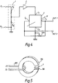
voltage conversion circuit 1 comprising a voltage divider circuit with resistors RA and RB, and is input to a voltage-current conversion circuit 2. Voltage-current conversion circuit 2 outputs a current proportional to the input voltage to control current terminal T1 ofHall element 3. Meanwhile, the current from the system under measurement is input to terminals 1S, 1L ofcurrent coil 105 wound onmagnetic material core 104 shown in Fig. 5, so that a magnetic field proportional to the input current is generated ingap 106. As a result, a Hall electromotive force Ey given by expression (1) is generated at voltage output terminals T3, T4 ofHall element 3, which is positioned so as to be at right angles to the magnetic field ofgap 106 and to the direction of flow of the control current ofHall element 3 which is from terminal T1 to terminal T2.
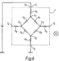
where Rh is the Hall coefficient, Bz is the magnetic field intensity, and Jx is the current density. In Fig. 4, the direction of the magnetic field is shown as an arrow x. Variable resistor VR1 is connected between voltage output terminals T3, T4 and serves to compensate for the offset voltage generated by the asymmetry of the characteristic ofHall element 3. Its moving contact is connected to ground together with control current terminal T2. Output terminals OUT1 and OUT2 of the power multiplication circuit are connected to voltage output terminals T3 and T4, respectively. - Next, the mechanism of offset voltage generation will be described with reference to the internal equivalent circuit of
Hall element 3 shown in Fig. 6. The equivalent circuit is expressed by a resistance bridge circuit, as shown. The output voltage is given by expression (2), if the respective voltages at the nodes are taken as E1, E2, E3, and E4 when the voltage E0 is applied to terminal T1 and the bridge resistances are respectively R1, R2, R3 and R4.
- If the magnetic field is 0,

- So, E3 - E4 = 0.
- Though, in the above expressions (2) and (3), the voltage E0 and resistances R5, T6, R7 and R8 are not expressed positively, they are included in the voltages E1, E2, E3 and E4, and when
Hall element 3 is connected to a following circuit having a very high input impedance, the output voltage between terminals T3 and T4 ofHall element 3 is nearly equal to the voltage (E3 - E4) expressed in the expression (2). - However, if for example resistance R1 fluctuates in the direction such that it is decreased by an amount r1,

- So, an offset voltage is generated between terminals T3 and T4 by the residual voltage even if the magnetic filed is 0.
- Next, the effect of the offset voltage when a magnetic field is present will be described. We assume that a magnetic field as shown in the Figure is applied to
Hall element 3 of Fig. 6, and that the resistances of resistors R1, R4 decrease while the resistances of resistors R2, R3 increase. The result of expressing graphically the potential difference between output voltage terminals T3, T4 is shown in Fig. 7 when a half-wave AC current flows between terminals T1, T2 for the four combinations of "positive"/"negative" direction of the magnetic field and "0 degrees/"180 degrees" of the phase of the control current. The upper row of diagrams in Fig. 7 indicates the waveform of the magnetic field intensity. The middle row indicates the waveform of the power source voltage of the system under measurement. The lower row indicates the waveform of the output voltage which is shown by broken lines in the case where there is no offset. If now we assume that the offset of resistor R1 is generated in the direction of decreasing resistance, the output voltage is decreased or increased by the amount of the offset voltage, as shown by the continuous line in the bottom row of Fig. 7. Accordingly, the output voltage is adjusted to zero in the condition where magnetic field is not applied by providing a variable resistor VR1 as shown in Fig. 4 to cancel the deviation of the output voltage produced by this offset voltage. - In the conventional power multiplication circuit described above, adjustment of the variable resistance in order to compensate the offset for fluctuations in the offset resistance produced by temperature change or occurring over a period of years was indispensable. However, for watt hour meters used by ordinary users this type of continuous adjustment operation is impracticable and occurrence of errors was therefore inevitable. Due to the need for a component having a mechanical contact part such as a variable resistor, there was also a reliability problem, and the power multiplication circuit was difficult to implement as an LSI.
- Accordingly, one objection of this invention is to provide a power multiplication circuit wherein fluctuation in the offset voltage due to temperature change or change over a period of years etc. can be automatically corrected.
- These and other objects of this invention may be achieved by providing a power multiplication circuit, comprising:
a Hall element for generating between voltage output terminals thereof a first output voltage corresponding to power of a system under measurement;
operating means connected to receive said first output voltage for amplifying said first output voltage and for changing over between amplified first output voltage and an inverted amplified first output voltage in alternate time periods corresponding to the length of a half cycle of said system under measurement to generate a second output voltage;
integrating means for integrating said second output voltage to generate an integrated signal; and
a variable resistance member connected between one of said voltage output terminals of said Hall element member and ground, and connected to receive said integrated signal, the resistance thereof being controlled by said integrated signal so as to compensate offset voltage of said Hall element member. - According to another aspect of this invention, there is further provided a power meter for detecting a power of a system. The power meter includes a voltage-current conversion circuit connected to receive a power source voltage of the system under measurement for converting the power source voltage to a control current proportional to the power source voltage and a Hall element. The Hall element is provided with control current input terminals and voltage output terminals and is positioned in a magnetic field such that a plane thereof created by the control current input terminals and the voltage output terminals is substantially perpendicular to the magnetic field. An intensity of the magnetic field is proportional to a current of the system under measurement. The Hall element is connected to the voltage-current conversion circuit such that the control current flows through the control current input terminals and generates a first output voltage corresponding to the power of said system under measurement between the voltage output terminals. The power meter further includes a voltage polarity detection circuit for detecting a polarity of the power source voltage of the system under measurement and an operating amplifier circuit connected to receive the first output voltage and for amplifying the first output voltage to generate amplified first output voltage and an inverted voltage of the amplified first output voltage. An output terminal of the power meter is connected to the operating amplifier circuit for outputting the amplified first output voltage as the power of the system under measurement. The power meter also includes a switch circuit connected to receive the amplified first output voltage, the inverted voltage and the polarity for changing over the amplified first output voltage and the inverted voltage to generate a second output voltage in accordance with the polarity and an integrating amplifier for integrating the second output voltage to generate an integrated signal. The power meter further includes a variable resistance element connected between one of the voltage output terminals of the Hall element and ground and connected to receive the integrated signal. A resistance thereof is changed by the integrated signal so that an offset voltage of the Hall element is reduced to zero.
- In this invention, by adopting the above means, the integrated value of the offset voltage is increased or decreased, with directionality, by arranging for the input to the integration circuit to be changed over in response to the polarity of the power source voltage of the system under measurement. The resistance of the variable resistor is thereby increased or decreased in response to the magnitude of the integrated value that is output by the integration circuit. This enables fluctuation of the offset resistance to be compensated such that the power can be calculated without offset.
- A more complete appreciation of the invention and many of the attendant advantages thereof will be readily obtained as the same becomes better understood by reference to the following detailed description when considered in connection with the accompanying drawings, wherein:
- Fig. 1 is a circuit diagram of a power multiplication circuit according to an embodiment of this invention;
- Fig. 2 is a waveform diagram of the various sub-units of the power multiplication circuit shown in Fig. 1;
- Fig. 3 is a circuit diagram of a power multiplication circuit according to another embodiment of this invention;
- Fig. 4 is a circuit diagram of a conventional power multiplication circuit;
- Fig. 5 is a layout diagram of a magnetic field generating unit;
- Fig. 6 is an equivalent circuit diagram of a Hall element; and
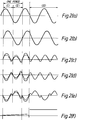
- Fig. 7 is a diagram given in explanation of the relationship between the Hall electromotive force and offset voltage.
- Referring now to the drawings, wherein like reference numerals designate identical or corresponding parts throughout the several views, embodiments of this invention will be described below.
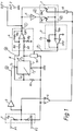
- Fig. 1 is a circuit diagram of a power multiplication circuit according to an embodiment of this invention. In Fig. 1, P1 and P2 are power source voltage input terminals that input the power source voltage, such as a.c. 100 volts of the system under measurement. A
voltage conversion circuit 1 converts the power source voltage input to input terminals P1 and P2 to a voltage suitable for matching the voltage in the power multiplication circuit by stepping up or stepping down. Thisvoltage conversion circuit 1 can be constituted using a voltage division circuit based on resistors RA, RB as shown in Fig. 1, or a transformer etc. A voltage-current conversion circuit 2 outputs a current proportional to the output voltage ofvoltage conversion circuit 1 at output terminal la. AHall element 3 is provided with control current input terminals T1, T2 that input the current output from voltage-current conversion circuit 2, and with voltage output terminals T3, T4 that output the voltage obtained by the Hall effect. The construction is such thatHall element 3 is held ingap 106 ofmagnetic material core 104 around whichcurrent coil 105 is wound as shown in Fig. 5, and the-plane- containing control current input terminals T1, T2 and voltage output terminals T3, T4 is perpendicular to the magnetic field generated in thegap 106. The direction of the magnetic field is shown as an arrow x in Fig. 1. A subtractingamplifier 4 receives the AC voltages that are output at voltage output terminals T3, T4 ofHall element 3, and outputs the difference of the AC voltage to output terminal OUT1 of the power multification circuit. Output terminal OUT2 thereof is connected to ground. Asign inverting amplifier 5 inverts the polarity of the voltage applied from subtractingamplifier 4. A voltage polarity detection circuit 6 is connected between input terminal P2 and output terminal la ofvoltage conversion circuit 1 that ascertains the polarity of the power source voltage of the system that is the subject of measurement. - The output of voltage polarity detection circuit 6 is used such that if the ascertained polarity is positive a switch SW1 is closed and a switch SW2 is opened through an inverter 8, and if the ascertained polarity is negative switch SW1 is opened and switch SW2 is closed through inverter 8.
- Switches SW1 and SW2 in a switch circuit 7 are respectively switches that are put in the closed condition by an input signal of level "1" and put in the open condition by an input signal of level "0". The primary side of switch SW1 is connected to the output of
sign inverting amplifier 5, while the primary side of switch SW2 is connected to the output of subtractingamplifier 4. An integrating amplifier 9 integrates the voltage output from the secondary side of switches SW1, SW2. A variable resistance element 10 is connected between ground and voltage output terminal T3, so that its resistance value is controlled by the output of integrating amplifier 9. It may be implemented using an FET or Cds photocoupler etc. Rc is a resistor connected between voltage output terminal T4 and ground and is provided to take account of the case where the offset resistance r1 is negative. - Subtracting
amplifier 4 is constructed, for example, by an operational amplifier OP1 and resistors Rd, Re, Rf and Rg. Integrating amplifier 9 is constructed, for example, by an operational amplifier OP2, a resistor Rh and a capacitor Ca. - Next, the operation of the circuit constructed as above will be described. The power source voltage of the system under measurement that is input to power source voltage input terminals P1, P2 is converted to the suitable voltage by
voltage conversion circuit 1, which is input to voltage-current conversion circuit 2. The current obtained by converting the input voltage to a current proportional to it in voltage-current conversion circuit 2 flows intoHall element 3 from the control current input terminal T1 to terminal T2 ofHall element 3. Meanwhile, the current of the system under measurement is made to flow tocurrent coil 105 ofmagnetic material core 104, producing a magnetic field ingap 106 the intensity of which is proportional to the current of the system under measurement. This therefore results in the generation of a Hall electromotive force given by expression (1) at voltage output terminals T3, T4 ofHall element 3. The output voltage difference across voltage output terminals T3, T4 is therefore proportional to the product of the voltage and the current of the system under measurement. In other words, it is proportional to the power of the system under measurement. Subtractingamplifier 4 differentially amplifies its two inputs from voltage output terminals T3, T4 so that the output voltage difference across these voltage output terminals T3, T4 is output to the outside from output terminals OUT1 and OUT2 as the power value of the system under measurement. In general, the switch circuit 7 is used to change the input to integrating amplifier 9, between the output ofamplifier 4 and the inverted output ofamplifier 4 provided byinverter 5, in alternate time periods corresponding to the length of a half cycle of the power supply. In the embodiment illustrated, the polarity of the power source voltage of the system under measurement, which has been subjected to voltage conversion involtage conversion circuit 1, is ascertained by voltage polarity detection circuit 6. The ascertained polarity is used by switch circuit 7 to change over the phase of the output voltage of subtractingamplifier 4 which is input to integrating amplifier 9. The operation is such that, for example, if the polarity of the power source voltage of the system under measurement is positive, switch SW1 is closed and switch SW2 is opened, so that an output voltage ofsign inverting amplifier 5 in which the polarity of output voltage of subtractingamplifier 4 is inverted is input to integrating amplifier 9. In the opposite situation, if the polarity of the power source voltage of the system under measurement is negative, switch SW1 is opened and switch SW2 is closed, with the result that the output voltage of subtractingamplifier 4 is directly input to integrating amplifier 9 without inversion of polarity. Integrating amplifier 9 integrates the output voltage of switch circuit 7 and outputs the results to variable resistance element 10. Variable resistance element 10 changes its resistance in the direction such as to compensate for the offset voltage, this change being made in accordance with the sign and the magnitude of the input voltage. In other embodiments the polarity of the current may be used to change between the inverted and non-inverted outputs ofamplifier 4. - Next, typical waveforms at various locations of the power multiplication circuit on input of a sign wave will be described with reference to Fig. 2. The magnetic field intensity in
gap 106 ofmagnetic material core 104 is shown at (a). The current waveform of the output from voltage-current conversion circuit 2 that is input toHall element 3 is shown at (b). The waveform of the output of subtractingamplifier 4 is shown at (c). In (c), (d) and (e) of Fig. 2, the waveform when there is no offset is shown by a broken line, while the waveform when offset is present is shown by a continuous line. All of these waveforms are generated in accordance with the rules of combination of direction of magnetic field and polarity of the current shown in Fig. 7. The output waveform ofsign inverting amplifier 5 is shown at (d) and is arrived at by inverting the waveform of (c). The waveform of the output of switch circuit 7 is shown at (e) and is obtained by operating switch circuit 7 by means of voltage polarity detection circuit 6 in response to the power source voltage of the system under measurement; it is also the waveform of the input to integrating amplifier 9. During the period indicated by (I) in the Figure, the output voltage ofsign inverting amplifier 5 shown in (d) is input to integrating amplifier 9 by the closure of switch SW1. Also, in the period indicated by (II) in the Figure, the output voltage of subtractingamplifier 4 shown in (c) is input to integrating amplifier 9 by the closure of switch SW2. When there is no offset, the waveform expressed by a broken line in (e) in period (I) has the opposite polarity but equal magnitude to the waveform expressed by a broken line in (e) in period (II), so the output of integrating amplifier 9 is zero when integrated over one period including the period (I) and the period (II). When the offset resistance r1 (r1 > 0) is present inHall element 3, since the waveform, shown by the continuous line in (e), is offset in the negative direction, the output integrated by integrating amplifier 9, as shown in (f), is not zero. - Variable resistance element 10 is controlled based on the output of the integrating amplifier 9 as follows.
- The resistance of variable resistance element 10 decreases as the output voltage of integrating amplifier 9 increases, until it reaches a resistance that compensates the offset resistance r1 of
Hall element 3. The input voltage waveform of integrating amplifier 9 then has a waveform as shown by the broken line in (e). The output of integrating amplifier 9, does not further change, and the resistance of variable resistance element 10 is then maintained unaltered in this condition, in the state of period (III). Resistor Rc is required to effect compensation in the case where offset resistance r1 is negative. - With the embodiment described above, the offset voltage generated by change in the characteristic of
Hall element 3 can be automatically corrected, so that the power can be calculated accurately. - Fig. 3 is a circuit diagram showing a power multification circuit according to another embodiment of this invention. The same benefits as in the first embodiment can be obtained by employing two
amplifiers amplifier 4, by connecting operational amplifier 11 to voltage output terminal T4 ofHall element 3, and holding voltage output terminal T4 at ground level. - In the embodiments shown in Fig. 1 and Fig. 3, inverter 8 is used for controlling switch SW2. But this invention is not limited to these embodiments. In the case that switch SW2 is a switch that is put in the open condition by an input signal of level "1" and put in the closed condition by an input signal of level "0", inverter 8 can be omitted and switch SW2 is controlled directly by the output of voltage polarity detection circuit 6. Also, although in order to facilitate understanding of the operation in Fig. 1 and Fig. 3, switch circuit 7 is expressed by a circuit having a mechanical contact, a contact-less switch, such as a semiconductor switch, could of course be used.
- As described above, with this invention, a power multiplication circuit can be provided which is of high accuracy and wherein fluctuations of the offset voltage produced by temperature change and change over a period of years can be automatically corrected.
- Furthermore, since mechanical parts may be eliminated, it may easily be implemented as an LSI, enabling high reliability to be attained. Additionally, operation is simplified in that there is no need for initial adjustment.
- Obviously, numerous modifications and variations of the present invention are possible in light of the above teachings. It is therefore to be understood that within the scope of the appended claims, the invention may be practiced otherwise than as specifically described herein.
Claims (11)
- A power multiplication circuit, comprising:
a Hall element member for generating between voltage output terminals thereof a first output voltage corresponding to power of a system under measurement;
operating means connected to receive said first output voltage for amplifying said first output voltage and for changing over between amplified first output voltage and an inverted amplified first output voltage in alternate time periods corresponding to the length of a half cycle of said system under measurement to generate a second output voltage;
integrating means for integrating said second output voltage to generate an integrated signal; and
a variable resistance member connected between one of said voltage output terminals of said Hall element member and ground, and connected to receive said integrated signal, the resistance thereof being controlled by said integrated signal, so as to compensate offset voltage of said Hall element member. - A power multiplication circuit as claimed in claim 1, including polarity detection means for detecting the polarity of the voltage or current of the system, for controlling the operating means to change over between said amplified first output voltage and said inverter amplified first voltage in accordance with said detected polarity.
- A power multiplication circuit according to Claim 2, wherein said operating means includes:
subtracting amplifier means connected to said Hall element member for detecting different between voltages at said voltage output terminals of said Hall element member and for amplifying said difference to generate as said amplified first output voltage;
inverting amplifier means connected to said subtracting amplifier means for inverting said amplified first output voltage to generate said inverted amplified first output voltage;
switch means connected to receive said amplified first output voltage, said inverted voltage and said detected polarity for changing over between said amplified first output voltage and said inverted voltage to generate said second output voltage in accordance with said polarity. - A power multiplication circuit according to Claim 3:
wherein said switch means includes,
a first switch having a first terminal and a second terminal, said first terminal being connected to an output terminal of said inverting amplifier means, said second terminal being connected to an input terminal of said integrating amplifier means,
a second switch having a third terminal and a fourth terminal, said third terminal being connected to an output terminal of said subtracting amplifier means, said fourth terminal being connected to said input terminal of said integrating amplifier means, and
inverter means for inverting said polarity of said power source voltage; and
wherein said polarity is detected positive said first switch is closed and said second switch is opened via said inverter means and said switch means outputs said inverted voltage as said second output voltage, and when said detected polarity is negative said first switch is opened and said second switch is closed via said inverter means and said switch means outputs said amplified first output voltage as said second output voltage. - A power multiplication circuit according to Claim 4, wherein each of said first and second switches includes a mechanical switch.
- A power multiplication circuit according to Claim 4, wherein each of said first and second switches includes a semiconductor switch.
- The power multiplication circuit according to Claim 1 or 2:
wherein said switch means includes,
first amplifier means connected to a first voltage output terminal of said Hall element member for amplifying said first output voltage to generate said amplified first output voltage,
second amplifier means connected to said first voltage output terminal of said Hall element member for-amplifying said first output voltage to generate said inverted voltage of said amplified first output voltage, and
switch means connected to receive said amplified first output voltage, said inverted voltage and said polarity for changing over between said amplified first output voltage and said inverted voltage to generate said second output voltage in accordance with said polarity; and
wherein second voltage output terminal of said Hall element member is connected to said ground. - A power multiplication circuit according to Claim 7 when appendent to claim 2,
wherein said switch means includes,
a first switch having a first terminal and a second terminal, said first terminal being connected to an output terminal of said second amplifier means, said second terminal being connected to an input terminal of said integrating amplifier means,
a second switch having a third terminal and a fourth terminal, said third terminal being connected to an output terminal of said first amplifier means, said fourth terminal being connected to said input terminal of said integrating amplifier means, and
inverter means for inverting said polarity of said power source voltage; and
wherein when said polarity is positive said first switch is closed and said second switch is opened via said inverter means and said switch means outputs said inverted voltage as said second output voltage, and when said polarity is negative said first switch is opened and said second switch is closed via said inverter means and said switch means outputs said amplified first output voltage as said second output voltage. - A power multiplication circuit according to Claim 8, wherein each of said first and second switches includes a mechanical switch.
- A power multiplication circuit according to Claim 8, wherein each of said first and second switches includes a semiconductor switch.
- A power meter for detecting a power of a system, comprising:
a voltage-current conversion circuit connected to receive a power source voltage of said system under measurement for converting said power source voltage to a control current proportional to said power source voltage;
a Hall element having control current input terminals and voltage output terminals, positioned in a magnetic field such that a plane thereof created by said control current input terminals and said voltage output terminals is substantially perpendicular to said magnetic field;
intensity of said magnetic field being proportional to a current of said system under measurement;
said Hall element being connected to said voltage-current conversion circuit such that said control current flows through said control current input terminals and generating a first output voltage corresponding to said power of said system under measurement between said voltage output terminals;
voltage or current polarity detection circuit for detecting the polarity of said power source voltage or current of said system under measurement;
an operating amplifier circuit connected to receive said first output voltage and for amplifying said first output voltage to generate amplified first output voltage and an inverted voltage of said amplified first output voltage;
an output terminal connected to said operating amplifier circuit for outputting said amplified first output voltage as said power of said system under measurement;
a switch circuit connected to receive said amplified first output voltage, said inverted voltage and said polarity for changing over said amplified first output voltage and said inverted voltage to generate a second output voltage in accordance with said detected polarity;
an integrating amplifier for integrating said second output voltage to generate an integrated signal; and
a variable resistance element connected between one of said voltage output terminals of said Hall element and ground, and connected to receive said integrated signal, a resistance thereof being changed by said integrated signal to compensate offset voltage of said Hall element.
Applications Claiming Priority (3)
| Application Number | Priority Date | Filing Date | Title |
|---|---|---|---|
| JP330844/92 | 1992-12-11 | ||
| JP33084492 | 1992-12-11 | ||
| JP4330844A JP3011559B2 (en) | 1992-12-11 | 1992-12-11 | Power multiplication circuit |
Publications (2)
| Publication Number | Publication Date |
|---|---|
| EP0601817A1 true EP0601817A1 (en) | 1994-06-15 |
| EP0601817B1 EP0601817B1 (en) | 2004-11-17 |
Family
ID=18237171
Family Applications (1)
| Application Number | Title | Priority Date | Filing Date |
|---|---|---|---|
| EP93309774A Expired - Lifetime EP0601817B1 (en) | 1992-12-11 | 1993-12-06 | Power calculation circuit |
Country Status (5)
| Country | Link |
|---|---|
| US (1) | US5438258A (en) |
| EP (1) | EP0601817B1 (en) |
| JP (1) | JP3011559B2 (en) |
| KR (1) | KR0125595B1 (en) |
| DE (1) | DE69333695T2 (en) |
Cited By (2)
| Publication number | Priority date | Publication date | Assignee | Title |
|---|---|---|---|---|
| EP0635726A2 (en) * | 1993-07-21 | 1995-01-25 | Kabushiki Kaisha Toshiba | Power calculating device |
| WO1996028739A1 (en) * | 1995-03-16 | 1996-09-19 | Horstmann Timers & Controls Limited | Electricity measurement apparatus |
Families Citing this family (10)
| Publication number | Priority date | Publication date | Assignee | Title |
|---|---|---|---|---|
| JPH11352157A (en) * | 1998-06-11 | 1999-12-24 | Yazaki Corp | Power source detecting method and device therefor |
| US6392400B1 (en) * | 1998-10-08 | 2002-05-21 | Schlumberger Resource Management Services | High linearity, low offset interface for Hall effect devices |
| US6483291B1 (en) * | 2000-05-26 | 2002-11-19 | Chander P. Bhateja | Apparatus for measuring electrical power consumption |
| JP4579523B2 (en) * | 2003-09-30 | 2010-11-10 | 株式会社エルポート | Magnetic bridge type power sensor |
| US7579816B2 (en) * | 2006-02-07 | 2009-08-25 | Linear Technology Corporation | Single feedback input for regulation at both positive and negative voltage levels |
| JP4785627B2 (en) * | 2006-06-08 | 2011-10-05 | 三洋電機株式会社 | Electric vehicle leakage detection circuit and electric vehicle leakage detection method |
| US7825665B1 (en) * | 2007-03-14 | 2010-11-02 | Linear Technology Corporation | Feedback circuitry and methodology for switching circuit capable of generating both positive and negative output voltages |
| JP2018091626A (en) * | 2015-04-16 | 2018-06-14 | パナソニックIpマネジメント株式会社 | Electric leak detection device |
| JP2017058376A (en) * | 2016-11-10 | 2017-03-23 | 株式会社リコー | Power sensing sensor |
| CN115184668A (en) * | 2022-07-22 | 2022-10-14 | 核工业西南物理研究院 | Microwave power measurement method and system based on Hall effect |
Citations (6)
| Publication number | Priority date | Publication date | Assignee | Title |
|---|---|---|---|---|
| JPS5834365A (en) * | 1981-08-26 | 1983-02-28 | Hioki Denki Kk | Compensating method for rectified error voltage of hall element of clamp type wattmeter |
| GB2107070A (en) * | 1981-08-20 | 1983-04-20 | Standard Telephones Cables Ltd | Hall effect switch |
| DE3235188A1 (en) * | 1982-09-23 | 1984-03-29 | Kernforschungsanlage Jülich GmbH, 5170 Jülich | CIRCUIT WITH HALL FIELD PROBE |
| FR2594230A1 (en) * | 1986-02-10 | 1987-08-14 | Landis & Gyr Ag | DEVICE FOR MEASURING ELECTRIC POWER |
| DE3723268A1 (en) * | 1986-07-15 | 1988-01-28 | Iskra Sozd Elektro Indus | WATTMETER WITH A HALL SENSOR AND A / D CONVERTER |
| GB2199411A (en) * | 1986-12-06 | 1988-07-06 | Omega Electric Ltd | Auto compensating alternating current meter |
Family Cites Families (5)
| Publication number | Priority date | Publication date | Assignee | Title |
|---|---|---|---|---|
| CH651671A5 (en) * | 1980-12-24 | 1985-09-30 | Landis & Gyr Ag | Arrangement for measuring electrical performance or power. |
| US4608533A (en) * | 1983-06-22 | 1986-08-26 | Electric Power Research Institute, Inc. | Automatic compensation circuit for use with analog multiplier |
| US4808918A (en) * | 1986-04-09 | 1989-02-28 | Iskra-Sozd Elektrokovinske Industrije N.Sol.O. | Watthour meter comprising a Hall sensor and a voltage-frequency converter for very low voltages |
| CH677036A5 (en) * | 1987-08-06 | 1991-03-28 | Landis & Gyr Betriebs Ag | |
| YU238387A (en) * | 1987-12-24 | 1990-10-31 | Iskra | Gauge of electric power - energy with hall's sensor |
-
1992
- 1992-12-11 JP JP4330844A patent/JP3011559B2/en not_active Expired - Fee Related
-
1993
- 1993-07-30 US US08/099,535 patent/US5438258A/en not_active Expired - Lifetime
- 1993-12-06 DE DE69333695T patent/DE69333695T2/en not_active Expired - Fee Related
- 1993-12-06 EP EP93309774A patent/EP0601817B1/en not_active Expired - Lifetime
- 1993-12-09 KR KR1019930026962A patent/KR0125595B1/en not_active IP Right Cessation
Patent Citations (6)
| Publication number | Priority date | Publication date | Assignee | Title |
|---|---|---|---|---|
| GB2107070A (en) * | 1981-08-20 | 1983-04-20 | Standard Telephones Cables Ltd | Hall effect switch |
| JPS5834365A (en) * | 1981-08-26 | 1983-02-28 | Hioki Denki Kk | Compensating method for rectified error voltage of hall element of clamp type wattmeter |
| DE3235188A1 (en) * | 1982-09-23 | 1984-03-29 | Kernforschungsanlage Jülich GmbH, 5170 Jülich | CIRCUIT WITH HALL FIELD PROBE |
| FR2594230A1 (en) * | 1986-02-10 | 1987-08-14 | Landis & Gyr Ag | DEVICE FOR MEASURING ELECTRIC POWER |
| DE3723268A1 (en) * | 1986-07-15 | 1988-01-28 | Iskra Sozd Elektro Indus | WATTMETER WITH A HALL SENSOR AND A / D CONVERTER |
| GB2199411A (en) * | 1986-12-06 | 1988-07-06 | Omega Electric Ltd | Auto compensating alternating current meter |
Non-Patent Citations (1)
| Title |
|---|
| PATENT ABSTRACTS OF JAPAN vol. 7, no. 113 (P - 197) 18 May 1983 (1983-05-18) * |
Cited By (5)
| Publication number | Priority date | Publication date | Assignee | Title |
|---|---|---|---|---|
| EP0635726A2 (en) * | 1993-07-21 | 1995-01-25 | Kabushiki Kaisha Toshiba | Power calculating device |
| EP0635726A3 (en) * | 1993-07-21 | 1995-09-27 | Toshiba Kk | Power calculating device. |
| WO1996028739A1 (en) * | 1995-03-16 | 1996-09-19 | Horstmann Timers & Controls Limited | Electricity measurement apparatus |
| AU702196B2 (en) * | 1995-03-16 | 1999-02-18 | Horstmann Timers & Controls Limited | Electricity measurement apparatus |
| US6037763A (en) * | 1995-03-16 | 2000-03-14 | Horstmann Timers & Controls Limited | Electricity measurement apparatus using hall effect sensor having rectified bias current |
Also Published As
| Publication number | Publication date |
|---|---|
| DE69333695D1 (en) | 2004-12-23 |
| KR0125595B1 (en) | 1998-07-15 |
| JPH06174765A (en) | 1994-06-24 |
| JP3011559B2 (en) | 2000-02-21 |
| US5438258A (en) | 1995-08-01 |
| DE69333695T2 (en) | 2005-03-31 |
| KR940015517A (en) | 1994-07-21 |
| EP0601817B1 (en) | 2004-11-17 |
Similar Documents
| Publication | Publication Date | Title |
|---|---|---|
| US4596950A (en) | Compensated transducer | |
| US4315212A (en) | Electronic watthour meter | |
| EP0601817A1 (en) | Power multiplication circuit | |
| US4217546A (en) | Electronic energy consumption meter and system with automatic error correction | |
| GB1528984A (en) | Alternating current transformers | |
| US4761605A (en) | Input switching in electronic watthour meter | |
| EP0052981B1 (en) | Hall element circuit arranged to eliminate in-phase voltage | |
| EP0670502B1 (en) | Electrical quantity measurement device | |
| EP0635726B1 (en) | Power calculating device | |
| JPH02186284A (en) | Magnetic flux sensor used in magnetic field for detecting flux density | |
| US4672236A (en) | Voltage-to-frequency converter circuit | |
| JP2006504961A (en) | Device for measuring current intensity | |
| US4461987A (en) | Current sensing circuit for motor controls | |
| US3016493A (en) | Electric-signal converting apparatus | |
| JP3068977B2 (en) | Power multiplication circuit | |
| EP0067153B1 (en) | Dual core magnetic amplifier sensor | |
| JPS6139948Y2 (en) | ||
| SU1408426A1 (en) | Direct-current stabilizer | |
| JP3496899B2 (en) | Hall element and power multiplying circuit using the same | |
| JP3874577B2 (en) | Voltage controlled oscillator circuit | |
| US4710652A (en) | Interference signal component compensation circuit | |
| SU1725139A1 (en) | Current sensor | |
| SU1597755A1 (en) | D.c.transformer | |
| RU2035046C1 (en) | Rectifier that measures voltage level | |
| JP3147486B2 (en) | Semiconductor element measurement circuit |
Legal Events
| Date | Code | Title | Description |
|---|---|---|---|
| PUAI | Public reference made under article 153(3) epc to a published international application that has entered the european phase |
Free format text: ORIGINAL CODE: 0009012 |
|
| 17P | Request for examination filed |
Effective date: 19931217 |
|
| AK | Designated contracting states |
Kind code of ref document: A1 Designated state(s): CH DE FR GB LI |
|
| 17Q | First examination report despatched |
Effective date: 19980813 |
|
| GRAP | Despatch of communication of intention to grant a patent |
Free format text: ORIGINAL CODE: EPIDOSNIGR1 |
|
| RTI1 | Title (correction) |
Free format text: POWER CALCULATION CIRCUIT |
|
| GRAS | Grant fee paid |
Free format text: ORIGINAL CODE: EPIDOSNIGR3 |
|
| GRAA | (expected) grant |
Free format text: ORIGINAL CODE: 0009210 |
|
| AK | Designated contracting states |
Kind code of ref document: B1 Designated state(s): CH DE FR GB LI |
|
| REG | Reference to a national code |
Ref country code: GB Ref legal event code: FG4D |
|
| REG | Reference to a national code |
Ref country code: CH Ref legal event code: EP |
|
| REF | Corresponds to: |
Ref document number: 69333695 Country of ref document: DE Date of ref document: 20041223 Kind code of ref document: P |
|
| REG | Reference to a national code |
Ref country code: CH Ref legal event code: NV Representative=s name: ISLER & PEDRAZZINI AG |
|
| ET | Fr: translation filed | ||
| PLBE | No opposition filed within time limit |
Free format text: ORIGINAL CODE: 0009261 |
|
| STAA | Information on the status of an ep patent application or granted ep patent |
Free format text: STATUS: NO OPPOSITION FILED WITHIN TIME LIMIT |
|
| 26N | No opposition filed |
Effective date: 20050818 |
|
| REG | Reference to a national code |
Ref country code: GB Ref legal event code: 746 Effective date: 20070318 |
|
| REG | Reference to a national code |
Ref country code: CH Ref legal event code: PCAR Free format text: ISLER & PEDRAZZINI AG;POSTFACH 1772;8027 ZUERICH (CH) |
|
| PGFP | Annual fee paid to national office [announced via postgrant information from national office to epo] |
Ref country code: CH Payment date: 20081216 Year of fee payment: 16 |
|
| PGFP | Annual fee paid to national office [announced via postgrant information from national office to epo] |
Ref country code: FR Payment date: 20081212 Year of fee payment: 16 |
|
| PGFP | Annual fee paid to national office [announced via postgrant information from national office to epo] |
Ref country code: DE Payment date: 20081205 Year of fee payment: 16 |
|
| PGFP | Annual fee paid to national office [announced via postgrant information from national office to epo] |
Ref country code: GB Payment date: 20081203 Year of fee payment: 16 |
|
| REG | Reference to a national code |
Ref country code: CH Ref legal event code: PL |
|
| GBPC | Gb: european patent ceased through non-payment of renewal fee |
Effective date: 20091206 |
|
| REG | Reference to a national code |
Ref country code: FR Ref legal event code: ST Effective date: 20100831 |
|
| PG25 | Lapsed in a contracting state [announced via postgrant information from national office to epo] |
Ref country code: LI Free format text: LAPSE BECAUSE OF NON-PAYMENT OF DUE FEES Effective date: 20091231 Ref country code: FR Free format text: LAPSE BECAUSE OF NON-PAYMENT OF DUE FEES Effective date: 20091231 Ref country code: CH Free format text: LAPSE BECAUSE OF NON-PAYMENT OF DUE FEES Effective date: 20091231 |
|
| PG25 | Lapsed in a contracting state [announced via postgrant information from national office to epo] |
Ref country code: DE Free format text: LAPSE BECAUSE OF NON-PAYMENT OF DUE FEES Effective date: 20100701 |
|
| PG25 | Lapsed in a contracting state [announced via postgrant information from national office to epo] |
Ref country code: GB Free format text: LAPSE BECAUSE OF NON-PAYMENT OF DUE FEES Effective date: 20091206 |