EP0052981B1 - Hall element circuit arranged to eliminate in-phase voltage - Google Patents
Hall element circuit arranged to eliminate in-phase voltage Download PDFInfo
- Publication number
- EP0052981B1 EP0052981B1 EP81305346A EP81305346A EP0052981B1 EP 0052981 B1 EP0052981 B1 EP 0052981B1 EP 81305346 A EP81305346 A EP 81305346A EP 81305346 A EP81305346 A EP 81305346A EP 0052981 B1 EP0052981 B1 EP 0052981B1
- Authority
- EP
- European Patent Office
- Prior art keywords
- hall element
- control current
- operational amplifier
- terminal
- output
- Prior art date
- Legal status (The legal status is an assumption and is not a legal conclusion. Google has not performed a legal analysis and makes no representation as to the accuracy of the status listed.)
- Expired
Links
Images

Classifications
-
- G—PHYSICS
- G01—MEASURING; TESTING
- G01R—MEASURING ELECTRIC VARIABLES; MEASURING MAGNETIC VARIABLES
- G01R21/00—Arrangements for measuring electric power or power factor
- G01R21/08—Arrangements for measuring electric power or power factor by using galvanomagnetic-effect devices, e.g. Hall-effect devices
-
- G—PHYSICS
- G01—MEASURING; TESTING
- G01R—MEASURING ELECTRIC VARIABLES; MEASURING MAGNETIC VARIABLES
- G01R17/00—Measuring arrangements involving comparison with a reference value, e.g. bridge
- G01R17/02—Arrangements in which the value to be measured is automatically compared with a reference value
- G01R17/06—Automatic balancing arrangements
-
- G—PHYSICS
- G01—MEASURING; TESTING
- G01R—MEASURING ELECTRIC VARIABLES; MEASURING MAGNETIC VARIABLES
- G01R33/00—Arrangements or instruments for measuring magnetic variables
- G01R33/02—Measuring direction or magnitude of magnetic fields or magnetic flux
- G01R33/06—Measuring direction or magnitude of magnetic fields or magnetic flux using galvano-magnetic devices
- G01R33/07—Hall effect devices
Definitions
- This invention relates to a Hall element circuit arranged to eliminate the in-phase voltage.
- the Hall element which are used for magnetic sensors such as Gauss meters and the like, convert magnetic variation into electrical signal variation.
- the Hall element includes a semiconductor plate such as a GaAs, InSb, InAs, Ge or Si, having a pair of control current terminals for supplying a control current to the semiconductor plate and a pair of output terminals.
- a magnetic field is applied to the Hall element in a direction perpendicular to the control current direction while the control current is supplied to the Hall element, an output signal voltage (a Hall output voltage) corresponding to the magnitude of the magnetic field is produced at the output terminals.
- This output signal includes a certain D.C. voltage besides the Hall output voltage.
- This D.C. voltage is called "in-phase voltage” and is produced on account of a voltage drop between the control current terminal and the output terminals of the Hall element.
- a Hall element can be conceptualized as a network of four resistive elements having a common connection. When 'the connection is at a voltage other than ground, the in-phase voltage results. Accordingly, the in-phase voltage is generated independent of the application of the magnetic field.
- this in-phase voltage is much larger than the Hall output voltage.
- a GaAs Hall element having a sensitivity of 20 mV/mA-kG and an internal resistance 1 KQ produces a Hall output voltage of 20 mV, when a control current 1 mA and a magnetic field having a magnetic flux density 1 kG are applied to the Hall element.
- the Hall element also produces an in-phase voltage of 500 mV.
- the Hall output voltage biased by the in-phase voltage cannot be amplified sufficiently by an amplifier because the amplification ability of the amplifier cannot be utilized efficiently for amplifying the Hall output voltage. Accordingly, the in-phase voltage should be eliminated.
- CMRR common-mode rejection ratio
- a Hall element circuit arranged to eliminate the in-phase voltage of a Hall element, the circuit comprising a Hall element having first and second control current terminals and first and second output terminals; means for supplying a control current to said Hall element between said first and second control current terminals; and an operational amplifier having a first input terminal and a second input terminal which is connected to said first output terminal of said Hall element, and an output terminal; characterised in that the first input terminal of the operational amplifier is connected to ground potential, and the output terminal of the operational amplifier is connected to one of said first and second control current terminals, whereby said Hall element produces a Hall output voltage at its second output terminal.
- the second input terminal of the operational amplifier is also at the ground potential. This ensures that the first output terminal of the Hall element is also at ground potential. Therefore, no in-phase voltage is produced at the second output terminal of the Hall element.
- a Hall element circuit arranged to eliminate the in-phase voltage of a Hall element, the circuit comprising a Hall element having a pair of control current terminals and a pair of output terminals; a power source for feeding a control current between said pair of control current terminals of said Hall element; and an operational amplifier having a first input terminal and a second input terminal which is connected to one of said output terminals of said Hall element, and an output terminal; characterised in that the first input terminal of the operational amplifier is connected to ground potential, and the output terminal of the operational amplifier is connected to said power source, whereby said Hall element produces a Hall output voltage at its second output terminal.
- a Hall element 11 for example, a GaAs Hall element has first and second control currentterminals 11a and 11b, and first and second output terminals 11 and 11d.
- First control current input terminal 11a of Hall element 11 is connected to a constant current source 12.
- Second control current terminal 11b of Hall element 11 is connected to an output terminal of an operational amplifier 13.
- Operational amplifier 13, which is high gain direct-current amplifier, has inverted and non-inverted input terminals. The non-inverted input terminal of operational amplifier 13 is connected to ground. The inverted input terminal of operational amplifier 13 is connected to first output terminal 11c of Hall element 11.
- Non-inversion amplifier 14 includes an operational amplifier 15 which has a non-inverted input terminal connected to second output terminal 11d of Hall element 11 and an inverted input terminal connected to ground through a resistance 16. The output of operational amplifier 15 is fed back to the inverted input terminal thereof through a resistance 17 and also delivered to a voltage meter 18.
- a control current is supplied to Hall element 11 through first control current terminal 11a a from constant current source 12.
- supplied control current passes through Hall element 11 and then emerges from second control current terminal 11 b.
- This control current is drawn in operational amplifier 13.
- first output terminal 11c of Hall element 11 is at the ground potential. Accordingly, the in-phase voltage of Hall element 11 is eliminated automatically and accurately without using a differential amplifier.
- the circuit and magnetic sensors using Hall elements with this in-phase elimination have simple structures and low cost because it is not necessary to use variable resistors or highly accurate resistors.
- amplifier 14 connected to Hall element 11 is designed easily. Since first output terminal 11c of Hall element 11 is at the ground potential, the Hall output voltage varies about ground potential. Accordingly, the Hall output signal may have larger amplitude. For example, if a signal processing circuit connected to the output terminal of the Hall element has a power source voltage V, the Hall output signal may have an amplitude of approximately ⁇ V. This advantage is particularly useful when the circuit is operated by low power voltage.
- the circuit according to the present invention may feed twice as much control current to the Hall element as the prior art, when the control current is A.C. current. That is, the Hall element circuit with the in-phase voltage elimination of this invention has sensitivity twice as much as the prior art.
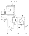
- Fig. 2 illustrates an A.C. watt meter circuit using a Hall element circuit with in-phase voltage elimination as shown in Fig. 1.
- A.C. voltage VL is delivered to a current source circuit 22 through a transformer 21.
- Current source circuit 22 converts the A.C. voltage VL to a current proportional to the magnitude of the A.C. voltage VL and then supplies it as a control current to first control current terminal 11 a of Hall element 11.
- a load current IL is converted to a magnetic field B proportional to the magnitude of the control current IL by a coil 24.
- Hall element 11 produces at second output terminal lid the product of the intensity of the magnetic field and the magnitude of the control current, i.e., the Hall output voltage of the consumed power which is the product of the load current IL and the A.C. voltage VL.
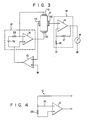
- Fig. 3 shows another constant current source type Hall element circuit with in-phase voltage elimination according to the present invention. This embodiment is similar to that illustrated in Fig. 1 except that current source 12 is connected between control current terminals 11 a and 11b, and the output of operational amplifier 13 is connected to current source 12.
- Current source 12 includes an operational amplifier 31, the inverted input terminal of which is connected to the first control current terminal 11a a and also connected to the positive pole of a D.C. power source 32 through a resistance 33.
- the non-inverted input terminal of operational amplifier 31 is connected to the negative pole of D.C. power source 32 and also connected to the output terminal of operational amplifier 13.
- control current from constant current source 12 passes through Hall element 11 and then flows into operational amplifier 31 of constant current source 12. Since the non-inverted input terminal of operational amplifier 13 is at ground potential, the inverted input terminal of operational amplifier 13 and first output terminal 11c of Hall element 11 are also at the ground potential. Accordingly, the in-phase voltage is eliminated like in the circuit shown in Fig. 1. In this circuit, operational amplifier 13 is perfectly prevented from overheating because the control current does not flow into operational amplifier 13.
- this constant current source 12 includes an operational amplifier 31.
- the inverted input terminal of operational amplifier 31 is to be connected to control current terminal 11a of Hall element 11 through a D.C. power source 32 and also connected to the non-inverted input terminal of operational amplifier 31 through a resistance 33.
- the output terminal of operational amplifier 31 is to be connected to second control current terminal 11b of Hall element 11.
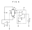
- Fig. 5 illustrates a Gauss meter circuit with a constant voltage source type Hall element circuit with in-phase voltage elimination according to the present invention.
- a Hall element 11 has first and second control current terminals 11a and 11b, and first and second output terminals 11c and 11d. Between first and second control current terminals 11a a and 11b of Hall element 11 a constant voltage source 30 is connected. Second control current terminal 11 b of Hall element 11 is also connected to an output terminal of an operational amplifier 13. Operational amplifier 13 has a non-inverted input terminal connected to ground and an inverted input terminal connected to first output terminal 11c of Hall element 11.
- the control current is fed from constant voltage source 30 to Hall element 11.
- the non-inverted input terminal of operational amplifier 13 is connected to ground. Accordingly, the inverted input terminal of operational amplifier, i.e., second output terminal 11c of Hall element 11 is at ground level. As a result, the in-phase voltage of Hall element 11 is automatically eliminated.
- magnetoelectric converters such as magnetic sensors or the like using Hall element employ a constant current source more frequently than a constant voltage source because the internal resistance of the Hall element is changed by variations of the temperature and the intensity of the magnetic field. Accordingly, the constant current source type is used for magnetoelectric converters requiring high accuracy. However, in a magnetoelectric converter which does not require high accuracy, the constant voltage source type as shown in Fig. 5 is useful.
Description
- This invention relates to a Hall element circuit arranged to eliminate the in-phase voltage.
- Hall elements, which are used for magnetic sensors such as Gauss meters and the like, convert magnetic variation into electrical signal variation. As well known, the Hall element includes a semiconductor plate such as a GaAs, InSb, InAs, Ge or Si, having a pair of control current terminals for supplying a control current to the semiconductor plate and a pair of output terminals. When a magnetic field is applied to the Hall element in a direction perpendicular to the control current direction while the control current is supplied to the Hall element, an output signal voltage (a Hall output voltage) corresponding to the magnitude of the magnetic field is produced at the output terminals.
- This output signal, however, includes a certain D.C. voltage besides the Hall output voltage. This D.C. voltage is called "in-phase voltage" and is produced on account of a voltage drop between the control current terminal and the output terminals of the Hall element. A Hall element can be conceptualized as a network of four resistive elements having a common connection. When 'the connection is at a voltage other than ground, the in-phase voltage results. Accordingly, the in-phase voltage is generated independent of the application of the magnetic field.
- Generally, this in-phase voltage is much larger than the Hall output voltage. For example, a GaAs Hall element having a sensitivity of 20 mV/mA-kG and an internal resistance 1 KQ produces a Hall output voltage of 20 mV, when a control current 1 mA and a magnetic field having a magnetic flux density 1 kG are applied to the Hall element. However, the Hall element also produces an in-phase voltage of 500 mV. The Hall output voltage biased by the in-phase voltage cannot be amplified sufficiently by an amplifier because the amplification ability of the amplifier cannot be utilized efficiently for amplifying the Hall output voltage. Accordingly, the in-phase voltage should be eliminated.
- One known method for eliminating the in-phase voltage of the Hall element is by employing a differential amplifier for cancelling the in-phase voltages produced at the pair of output terminals as described in US-A-4 199 696 and US-A-4 200 814. In US―A―4 199 696 there is disclosed a Hall element circuit as set out in the preambles of claims 1 and 5.
- This differential amplifier, however, should have a high common-mode rejection ratio (CMRR) in order to cancel the in-phase voltages accurately. To obtain a high CMRR the ratio of resistances used in the differential amplifier should be adjusted accurately by employing highly accurate resistances or variable resistances. Accordingly, an in-phase elimination circuit using a differential amplifier has a complicated structure and costs too much.
- It is an object of this invention to provide a relatively simple, low cost Hall element circuit arranged to eliminate in-phase voltage.
- It is another object of this invention to provide a Hall element circuit which can eliminate the in-phase voltage of the Hall element with high accuracy.
- According to one aspect of this invention, there is provided a Hall element circuit arranged to eliminate the in-phase voltage of a Hall element, the circuit comprising a Hall element having first and second control current terminals and first and second output terminals; means for supplying a control current to said Hall element between said first and second control current terminals; and an operational amplifier having a first input terminal and a second input terminal which is connected to said first output terminal of said Hall element, and an output terminal; characterised in that the first input terminal of the operational amplifier is connected to ground potential, and the output terminal of the operational amplifier is connected to one of said first and second control current terminals, whereby said Hall element produces a Hall output voltage at its second output terminal.
- As the first input terminal of the operational amplifier is at the ground potential, the second input terminal of the operational amplifier is also at the ground potential. This ensures that the first output terminal of the Hall element is also at ground potential. Therefore, no in-phase voltage is produced at the second output terminal of the Hall element.
- Preferred features of this aspect of this invention are set out in claims 2 to 4.
- According to another aspect of this invention there is provided a Hall element circuit arranged to eliminate the in-phase voltage of a Hall element, the circuit comprising a Hall element having a pair of control current terminals and a pair of output terminals; a power source for feeding a control current between said pair of control current terminals of said Hall element; and an operational amplifier having a first input terminal and a second input terminal which is connected to one of said output terminals of said Hall element, and an output terminal; characterised in that the first input terminal of the operational amplifier is connected to ground potential, and the output terminal of the operational amplifier is connected to said power source, whereby said Hall element produces a Hall output voltage at its second output terminal.
- Preferred features of this aspect of this invention are set out in claims 6 to 9.
- Preferred exemplary embodiments of the invention will now be described with reference to the accompanying drawings, in which:-
- Fig. 1 is a circuit diagram of a. Gauss meter using a Hall element circuit with a constant current source and in-phase voltage elimination according to the present invention;
- Fig. 2 is a circuit diagram of an A.C. watt meter using a Hall element and in-phase voltage elimination as shown in Fig. 1;
- Fig. 3 is a circuit diagram of a Gauss meter using a Hall element circuit with another of embodiment the constant source and in-phase voltage elimination according to the present invention;
- Fig. 4 is a circuit diagram of another type constant current source; and
- Fig. 5 is a circuit diagram of a Gauss meter using a Hall element circuit with a constant voltage source and in-phase voltage elimination according to the present invention.
- Referring to Fig. 1, a
Hall element 11, for example, a GaAs Hall element has first andsecond control currentterminals second output terminals 11 and 11d. First controlcurrent input terminal 11a ofHall element 11 is connected to a constantcurrent source 12. Second controlcurrent terminal 11b ofHall element 11 is connected to an output terminal of anoperational amplifier 13.Operational amplifier 13, which is high gain direct-current amplifier, has inverted and non-inverted input terminals. The non-inverted input terminal ofoperational amplifier 13 is connected to ground. The inverted input terminal ofoperational amplifier 13 is connected tofirst output terminal 11c ofHall element 11. - Second output terminal 11d is connected to a
non-inversion amplifier 14.Non-inversion amplifier 14 includes anoperational amplifier 15 which has a non-inverted input terminal connected to second output terminal 11d ofHall element 11 and an inverted input terminal connected to ground through aresistance 16. The output ofoperational amplifier 15 is fed back to the inverted input terminal thereof through aresistance 17 and also delivered to avoltage meter 18. - In operation, a control current is supplied to
Hall element 11 through first controlcurrent terminal 11a a from constantcurrent source 12. Thus supplied control current passes throughHall element 11 and then emerges from second controlcurrent terminal 11 b. This control current is drawn inoperational amplifier 13. - As is well known, when the non-inverted input terminal of
operational amplifier 13 is at the ground potential, the inverted input terminal ofoperational amplifier 13 is also at the ground level. Accordingly,first output terminal 11 c ofHall element 11 is also at the ground level. As a result, the Hall output voltage from which the in-phase voltage has been eliminated is produced at second output terminal 11 d. The thus obtained Hall output voltage is amplified bynon-inversion amplifier 14 and then delivered tovoltage meter 18. - As described above, in accordance with the embodiments of the present invention,
first output terminal 11c ofHall element 11 is at the ground potential. Accordingly, the in-phase voltage ofHall element 11 is eliminated automatically and accurately without using a differential amplifier. - As a result, the circuit and magnetic sensors using Hall elements with this in-phase elimination have simple structures and low cost because it is not necessary to use variable resistors or highly accurate resistors. Also,
amplifier 14 connected toHall element 11 is designed easily. Sincefirst output terminal 11c ofHall element 11 is at the ground potential, the Hall output voltage varies about ground potential. Accordingly, the Hall output signal may have larger amplitude. For example, if a signal processing circuit connected to the output terminal of the Hall element has a power source voltage V, the Hall output signal may have an amplitude of approximately ±V. This advantage is particularly useful when the circuit is operated by low power voltage. - For the same reason, the circuit according to the present invention may feed twice as much control current to the Hall element as the prior art, when the control current is A.C. current. That is, the Hall element circuit with the in-phase voltage elimination of this invention has sensitivity twice as much as the prior art.
- Fig. 2 illustrates an A.C. watt meter circuit using a Hall element circuit with in-phase voltage elimination as shown in Fig. 1. In Fig. 2, like reference characters designate similar parts to those of Fig. 1. A.C. voltage VL is delivered to a
current source circuit 22 through atransformer 21.Current source circuit 22 converts the A.C. voltage VL to a current proportional to the magnitude of the A.C. voltage VL and then supplies it as a control current to first controlcurrent terminal 11 a ofHall element 11. A load current IL is converted to a magnetic field B proportional to the magnitude of the control current IL by acoil 24. As a result,Hall element 11 produces at second output terminal lid the product of the intensity of the magnetic field and the magnitude of the control current, i.e., the Hall output voltage of the consumed power which is the product of the load current IL and the A.C. voltage VL. - Fig. 3 shows another constant current source type Hall element circuit with in-phase voltage elimination according to the present invention. This embodiment is similar to that illustrated in Fig. 1 except that
current source 12 is connected between controlcurrent terminals operational amplifier 13 is connected tocurrent source 12. -
Current source 12 includes anoperational amplifier 31, the inverted input terminal of which is connected to the first controlcurrent terminal 11a a and also connected to the positive pole of aD.C. power source 32 through aresistance 33. The non-inverted input terminal ofoperational amplifier 31 is connected to the negative pole ofD.C. power source 32 and also connected to the output terminal ofoperational amplifier 13. - The control current from constant
current source 12 passes throughHall element 11 and then flows intooperational amplifier 31 of constantcurrent source 12. Since the non-inverted input terminal ofoperational amplifier 13 is at ground potential, the inverted input terminal ofoperational amplifier 13 andfirst output terminal 11c ofHall element 11 are also at the ground potential. Accordingly, the in-phase voltage is eliminated like in the circuit shown in Fig. 1. In this circuit,operational amplifier 13 is perfectly prevented from overheating because the control current does not flow intooperational amplifier 13. - As an alternative to constant
current source 12 shown in Fig. 3 a constantcurrent source 12 shown in Fig. 4 may be employed. Referring to Fig. 4, this constantcurrent source 12 includes anoperational amplifier 31. The inverted input terminal ofoperational amplifier 31 is to be connected to control current terminal 11a ofHall element 11 through aD.C. power source 32 and also connected to the non-inverted input terminal ofoperational amplifier 31 through aresistance 33. The output terminal ofoperational amplifier 31 is to be connected to second control current terminal 11b ofHall element 11. - Fig. 5 illustrates a Gauss meter circuit with a constant voltage source type Hall element circuit with in-phase voltage elimination according to the present invention. In Fig. 5, like reference characters designate similar parts to those of Fig. 1. A
Hall element 11 has first and second controlcurrent terminals second output terminals 11c and 11d. Between first and second controlcurrent terminals 11a a and 11b ofHall element 11 aconstant voltage source 30 is connected. Second control current terminal 11 b ofHall element 11 is also connected to an output terminal of anoperational amplifier 13.Operational amplifier 13 has a non-inverted input terminal connected to ground and an inverted input terminal connected tofirst output terminal 11c ofHall element 11. - The control current is fed from
constant voltage source 30 toHall element 11. The non-inverted input terminal ofoperational amplifier 13 is connected to ground. Accordingly, the inverted input terminal of operational amplifier, i.e.,second output terminal 11c ofHall element 11 is at ground level. As a result, the in-phase voltage ofHall element 11 is automatically eliminated. - In general, magnetoelectric converters such as magnetic sensors or the like using Hall element employ a constant current source more frequently than a constant voltage source because the internal resistance of the Hall element is changed by variations of the temperature and the intensity of the magnetic field. Accordingly, the constant current source type is used for magnetoelectric converters requiring high accuracy. However, in a magnetoelectric converter which does not require high accuracy, the constant voltage source type as shown in Fig. 5 is useful.
Claims (9)
Applications Claiming Priority (4)
| Application Number | Priority Date | Filing Date | Title |
|---|---|---|---|
| JP55166409A JPS5790176A (en) | 1980-11-26 | 1980-11-26 | In-phase voltage removing circuit for hall element |
| JP166409/80 | 1980-11-26 | ||
| JP56056714A JPS57171211A (en) | 1981-04-15 | 1981-04-15 | Removing circuit for in-phase voltage of hall element |
| JP56714/81 | 1981-04-15 |
Publications (2)
| Publication Number | Publication Date |
|---|---|
| EP0052981A1 EP0052981A1 (en) | 1982-06-02 |
| EP0052981B1 true EP0052981B1 (en) | 1985-10-30 |
Family
ID=26397698
Family Applications (1)
| Application Number | Title | Priority Date | Filing Date |
|---|---|---|---|
| EP81305346A Expired EP0052981B1 (en) | 1980-11-26 | 1981-11-11 | Hall element circuit arranged to eliminate in-phase voltage |
Country Status (4)
| Country | Link |
|---|---|
| US (1) | US4435653A (en) |
| EP (1) | EP0052981B1 (en) |
| CA (1) | CA1195735A (en) |
| DE (1) | DE3172782D1 (en) |
Families Citing this family (13)
| Publication number | Priority date | Publication date | Assignee | Title |
|---|---|---|---|---|
| DE3235188C2 (en) * | 1982-09-23 | 1986-03-20 | Kernforschungsanlage Jülich GmbH, 5170 Jülich | Circuit for measuring magnetic induction with a Hall field probe |
| US4611129A (en) * | 1983-04-22 | 1986-09-09 | Nec Corporation | Signal conversion circuit |
| DE3322942C2 (en) * | 1983-06-25 | 1986-03-20 | Kernforschungsanlage Jülich GmbH, 5170 Jülich | Circuit for measuring magnetic induction with a Hall field probe |
| EP0357013A3 (en) * | 1988-09-02 | 1991-05-15 | Honeywell Inc. | Magnetic field measuring circuit |
| JP2796391B2 (en) * | 1990-01-08 | 1998-09-10 | 株式会社日立製作所 | Physical quantity detection method and physical quantity detection device, servo motor using these methods and devices, and power steering device using this servo motor |
| EP0438637A1 (en) * | 1990-01-24 | 1991-07-31 | Landis & Gyr Business Support AG | Method and apparatus for the determination of an effective value Ieff of a current to be measured using a Hall element and an amplifier circuit |
| US5686827A (en) * | 1996-02-09 | 1997-11-11 | Eaton Corporation | Temperature compensated Hall effect device |
| US6392400B1 (en) * | 1998-10-08 | 2002-05-21 | Schlumberger Resource Management Services | High linearity, low offset interface for Hall effect devices |
| NL1024114C1 (en) * | 2003-08-15 | 2005-02-16 | Systematic Design Holding B V | Method and device for taking measurements on magnetic fields using a hall sensor. |
| EP1679524A1 (en) * | 2005-01-11 | 2006-07-12 | Ecole Polytechnique Federale De Lausanne Epfl - Sti - Imm - Lmis3 | Hall sensor and method of operating a Hall sensor |
| US7847536B2 (en) * | 2006-08-31 | 2010-12-07 | Itron, Inc. | Hall sensor with temperature drift control |
| JP6144515B2 (en) * | 2013-03-27 | 2017-06-07 | 旭化成エレクトロニクス株式会社 | Hall element drive circuit |
| CN104571246B (en) * | 2014-12-17 | 2017-01-04 | 南京邮电大学 | A kind of rotatory current circuit being applied to Hall element |
Family Cites Families (3)
| Publication number | Priority date | Publication date | Assignee | Title |
|---|---|---|---|---|
| DE1490670A1 (en) * | 1964-09-26 | 1969-08-14 | Siemens Ag | Arrangement for balancing the zero voltage of Hall generators |
| US4200814A (en) * | 1976-11-05 | 1980-04-29 | Tokyo Shibaura Electric Co., Ltd. | Multiplier with hall element |
| DE2749784A1 (en) * | 1977-03-18 | 1978-09-21 | Tokyo Shibaura Electric Co | MULTIPLE CIRCUIT, IN PARTICULAR FOR WATT-HOUR METERS |
-
1981
- 1981-11-06 US US06/318,852 patent/US4435653A/en not_active Expired - Lifetime
- 1981-11-11 EP EP81305346A patent/EP0052981B1/en not_active Expired
- 1981-11-11 DE DE8181305346T patent/DE3172782D1/en not_active Expired
- 1981-11-24 CA CA000390760A patent/CA1195735A/en not_active Expired
Also Published As
| Publication number | Publication date |
|---|---|
| DE3172782D1 (en) | 1985-12-05 |
| CA1195735A (en) | 1985-10-22 |
| US4435653A (en) | 1984-03-06 |
| EP0052981A1 (en) | 1982-06-02 |
Similar Documents
| Publication | Publication Date | Title |
|---|---|---|
| US5146156A (en) | Current intensity transformer device for measuring a variable electric current | |
| EP0052981B1 (en) | Hall element circuit arranged to eliminate in-phase voltage | |
| GB1587870A (en) | Hall-effect integrated circuit | |
| GB1528984A (en) | Alternating current transformers | |
| US4200814A (en) | Multiplier with hall element | |
| JPS634717B2 (en) | ||
| JPH0661432A (en) | Semiconductor device | |
| EP0670502B1 (en) | Electrical quantity measurement device | |
| EP0601817A1 (en) | Power multiplication circuit | |
| EP0157447B1 (en) | Differential amplifier | |
| US4415865A (en) | Circuit arrangement for controlling the quiescent current in a class AB amplifier stage | |
| JP2004020455A (en) | Current detector | |
| US6339702B1 (en) | Output power detection circuit of transmitter | |
| EP0067153B1 (en) | Dual core magnetic amplifier sensor | |
| JPH0552872A (en) | Effective value level detector | |
| JP2938657B2 (en) | Current detection circuit | |
| KR850000358B1 (en) | In-phase voltage elimination circuit for hall element | |
| JP2000155139A (en) | Current detecting device | |
| RU2035046C1 (en) | Rectifier that measures voltage level | |
| KR910009926B1 (en) | Means power detecting circuit using hall cell | |
| JP2835093B2 (en) | DC current detector | |
| JPS6139948Y2 (en) | ||
| JPH08320346A (en) | Coulombmeter | |
| JPH077047B2 (en) | Magnetic detection device | |
| SU1691797A1 (en) | Device for non-contact measuring of current |
Legal Events
| Date | Code | Title | Description |
|---|---|---|---|
| PUAI | Public reference made under article 153(3) epc to a published international application that has entered the european phase |
Free format text: ORIGINAL CODE: 0009012 |
|
| 17P | Request for examination filed |
Effective date: 19811119 |
|
| AK | Designated contracting states |
Designated state(s): CH DE FR GB IT SE |
|
| RAP1 | Party data changed (applicant data changed or rights of an application transferred) |
Owner name: KABUSHIKI KAISHA TOSHIBA |
|
| GRAA | (expected) grant |
Free format text: ORIGINAL CODE: 0009210 |
|
| RBV | Designated contracting states (corrected) |
Designated state(s): DE FR GB |
|
| AK | Designated contracting states |
Designated state(s): DE FR GB |
|
| REF | Corresponds to: |
Ref document number: 3172782 Country of ref document: DE Date of ref document: 19851205 |
|
| ET | Fr: translation filed | ||
| PLBI | Opposition filed |
Free format text: ORIGINAL CODE: 0009260 |
|
| 26 | Opposition filed |
Opponent name: LGZ LANDIS & GYR ZUG AG Effective date: 19860313 |
|
| RDAG | Patent revoked |
Free format text: ORIGINAL CODE: 0009271 |
|
| STAA | Information on the status of an ep patent application or granted ep patent |
Free format text: STATUS: PATENT REVOKED |
|
| GBPR | Gb: patent revoked under art. 102 of the ep convention designating the uk as contracting state | ||
| 27W | Patent revoked |
Effective date: 19880716 |