EP0600353B1 - Automatischer Synchronisierschalter für Mehrfachbildwiedergabe - Google Patents
Automatischer Synchronisierschalter für Mehrfachbildwiedergabe Download PDFInfo
- Publication number
- EP0600353B1 EP0600353B1 EP93118871A EP93118871A EP0600353B1 EP 0600353 B1 EP0600353 B1 EP 0600353B1 EP 93118871 A EP93118871 A EP 93118871A EP 93118871 A EP93118871 A EP 93118871A EP 0600353 B1 EP0600353 B1 EP 0600353B1
- Authority
- EP
- European Patent Office
- Prior art keywords
- video
- signal
- synchronizing
- display
- signals
- Prior art date
- Legal status (The legal status is an assumption and is not a legal conclusion. Google has not performed a legal analysis and makes no representation as to the accuracy of the status listed.)
- Expired - Lifetime
Links
- 239000002131 composite material Substances 0.000 claims description 21
- 230000008878 coupling Effects 0.000 claims 1
- 238000010168 coupling process Methods 0.000 claims 1
- 238000005859 coupling reaction Methods 0.000 claims 1
- 238000010586 diagram Methods 0.000 description 10
- 239000003990 capacitor Substances 0.000 description 5
- 238000007906 compression Methods 0.000 description 5
- 230000006835 compression Effects 0.000 description 5
- 230000003044 adaptive effect Effects 0.000 description 4
- 230000006870 function Effects 0.000 description 3
- 238000012544 monitoring process Methods 0.000 description 2
- 230000001360 synchronised effect Effects 0.000 description 2
- 101710148588 ADP,ATP carrier protein 2 Proteins 0.000 description 1
- 101710165307 ADP,ATP carrier protein 2, mitochondrial Proteins 0.000 description 1
- 102100032533 ADP/ATP translocase 1 Human genes 0.000 description 1
- 102100026396 ADP/ATP translocase 2 Human genes 0.000 description 1
- 101710102718 ADP/ATP translocase 2 Proteins 0.000 description 1
- 101710102715 ADP/ATP translocase 3 Proteins 0.000 description 1
- 101150093547 AUX1 gene Proteins 0.000 description 1
- 101000768061 Escherichia phage P1 Antirepressor protein 1 Proteins 0.000 description 1
- 108010014173 Factor X Proteins 0.000 description 1
- 101000796932 Homo sapiens ADP/ATP translocase 1 Proteins 0.000 description 1
- 101100367246 Saccharomyces cerevisiae (strain ATCC 204508 / S288c) SWA2 gene Proteins 0.000 description 1
- 238000013144 data compression Methods 0.000 description 1
- 230000003111 delayed effect Effects 0.000 description 1
- 238000001514 detection method Methods 0.000 description 1
- 244000145841 kine Species 0.000 description 1
- 238000000034 method Methods 0.000 description 1
- 230000000750 progressive effect Effects 0.000 description 1
- 230000004044 response Effects 0.000 description 1
- 230000002441 reversible effect Effects 0.000 description 1
- 239000004576 sand Substances 0.000 description 1
Images


Classifications
-
- H—ELECTRICITY
- H04—ELECTRIC COMMUNICATION TECHNIQUE
- H04N—PICTORIAL COMMUNICATION, e.g. TELEVISION
- H04N5/00—Details of television systems
- H04N5/44—Receiver circuitry for the reception of television signals according to analogue transmission standards
- H04N5/445—Receiver circuitry for the reception of television signals according to analogue transmission standards for displaying additional information
- H04N5/45—Picture in picture, e.g. displaying simultaneously another television channel in a region of the screen
-
- H—ELECTRICITY
- H04—ELECTRIC COMMUNICATION TECHNIQUE
- H04N—PICTORIAL COMMUNICATION, e.g. TELEVISION
- H04N5/00—Details of television systems
- H04N5/04—Synchronising
Definitions
- the invention relates to the field of televisions capable of displaying side-by-side pictures of substantially equal size from different sources, and in particular, to such televisions having a wide display format ratio screen.
- Most televisions today have a format display ratio, horizontal width to vertical height, of 4:3.
- a wide format display ratio corresponds more closely to the display format ratio of movies, for example 16:9.
- the invention is applicable to both direct view televisions and projection televisions.
- a wide screen television disclosed in WO 91/19397, published December 12, 1991 and corresponding to PCT/US91/03746, is capable of providing high resolution, single and multiple picture displays, from single and multiple sources having similar or different format ratios, and with selectable display format ratios.
- Such television apparatus as disclosed in WO 91/19397 can display multiple pictures simultaneously, for example from two video sources.
- the video sources may be the tuner in the television, a tuner in a video cassette recorder, a video camera, and others.
- a display mode particularly suited for a wide screen television is side-by-side pictures of substantially the same size, from different video sources, for example two different channels.
- a wide screen television having a display format ratio (width to height) of 16:9 each of two side-by-side pictures of comparable size in a full screen display would have a format display ratio of 8:9.
- the 4:3 picture In order to fit a 4:3 picture into an 8:9 space, the 4:3 picture must be horizontally cropped or horizontally compressed, or some combination of both.
- the display In order to display two pictures side-by-side, the display is locked to one of two incoming signals, referred to as the first signal or first picture for convenience. This can be the left picture or the right picture in the side-by-side mode.
- the first picture may become nonfunctional.
- the television receiver could be tuned to a blank channel, or the television station could go off the air, or the video source could be interrupted. If the first picture becomes nonfunctional, the synchronization for the second picture is also lost. Without proper synchronization, the second picture will jitter.
- a video display system having means for simultaneously displaying pictures representative of first and second video signals, and means for selectively synchronizing the display with either of the first and second video signals.
- a display system for side-by-side pictures comprises a first circuit for separating a first composite synchronizing signal from a first video signal having a conventional format display ratio and a second circuit for separating a second composite synchronizing signal from a second video signal having the same conventional format display ratio.
- a detecting circuit senses the presence of the first video signal, by monitoring the horizontal synchronizing component thereof.
- a video display control circuit has a mode of operation in which pictures representative of the first and second video signals are displayed in side-by-side relationship and substantially without image aspect ratio distortion.
- a synchronization switch selects one of the first and second composite synchronizing signals for synchronizing the video display. The second composite synchronizing signal is automatically selected unless the horizontal synchronizing component of the first video signal is detected.
- the detecting circuit comprises a synchronizing component separator, a bandpass filter, and a detector.
- the detecting circuit When the first video signal is present, the horizontal synchronizing signal is separated and monitored.
- the detecting circuit generates an output signal indicating whether an adequate horizontal synchronizing component is present.
- the invention further comprises a microprocessor coupled to the detecting circuit and the automatic synchronization switch. The microprocessor controls the automatic synchronization switch output to be the second composite synchronizing signal when the first video signal is not detected by the detecting circuit.
- the invention further comprises a first signal processing means for speeding up the first video signal, a video display means synchronized with the automatic synchronization switch output, means for vertically synchronizing the second video signal with the first video signal and the video display means, a second signal processing means for speeding up said second video signal, and means for combining the first and second processed video signals for side-by-side display.
- the first and second signal processing means can crop and reduce picture size so that the first and second pictures can be displayed on a wide screen display.
- the second picture can be displayed in a side-by-side video display system despite the loss of the first picture.
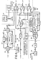
- FIGURE 1 is a block diagram of an automatic synchronization switch in a wide screen television.
- FIGURE 2 is a timing diagram of the composite video signal processed by the detecting circuit shown in FIGURE 1.
- FIGURE 3 is a circuit diagram of a sync separator and bandpass filter adapted to be used in the detecting circuit.
- FIGURE 4 is a circuit diagram of a detector with hysteresis adapted to be used in the detecting circuit.
- FIGURE 5 is a block diagram of the bandpass filter adapted to be used in the detecting circuit.
- FIGURE 6 illustrates the response of the bandpass filter of FIGURES 3 and 5.
- FIGURE 7 is a block diagram of a wide screen television adapted for operation at 2f H horizontal scanning.
- FIGURE 8 is a block diagram of the gate array of FIGURE 7, illustrating the main, auxiliary and output signal paths.
- FIGURE 7 An overall block diagram for a wide screen television apparatus in accordance with WO 91/19397, and adapted to operate with 2f H horizontal scanning, is shown in FIGURE 7 and generally designated 10.
- the television 10 generally comprises a video signals input section 20, a chassis or TV microprocessor (TV ⁇ P) 216, a wide screen processor 30, a 1f H to 2f H converter 40, a deflection circuit 50, an RGB interface 60, a YUV to RGB converter 240, kine drivers 242, direct view or projection tubes 244 and a power supply 70.
- the YUV to RGB converter 240 may be an industry type TA7730.
- the grouping of various circuits into different functional blocks is made for purposes of convenience in description, and is not intended as limiting the physical position of such circuits relative to one another.
- the video signals input section 20 is adapted for receiving a plurality of composite video signals from different video sources.
- the video signals may be selectively switched for display as main and auxiliary video signals.
- An RF switch 204 has two antenna inputs ANT1 and ANT 2. These represent inputs for both off-air antenna reception and cable reception.
- the RF switch 204 controls which antenna input is supplied to a first tuner 206 and to a second tuner 208.
- the output of first tuner 206 is an input to a one-chip 202, which performs a number of functions related to tuning, horizontal and vertical deflection and video controls.
- the particular one-chip shown is industry designated type TA7777.
- the baseband video signal VIDEO OUT developed in the one-chip and resulting from the signal from first tuner 206 is an input to both video switch 200 and the TV1 input of wide screen processor 30.
- Other baseband video inputs to video switch 200 are designated AUX1 and AUX 2. These might be used for video cameras, laser disc players, video tape players, video games and the like.
- the output of the video switch 200, which is controlled by the chassis or TV microprocessor 216 is designated SWITCHED VIDEO.
- the SWITCHED VIDEO is another input to wide screen processor 30.
- a switch SW1 wide screen processor selects between the TV1 and SWITCHED VIDEO signals as a SEL COMP OUT video signal which is an input to a Y/C decoder 210.
- the Y/C decoder 210 may be implemented as an adaptive line comb filter.
- Two further video sources S1 and S2 are also inputs to the Y/C decoder 210.
- Each of S1 and S2 represent different S-VHS sources, and each consists of separate luminance and chrominance signals.
- a switch which may be incorporated as part of the Y/C decoder, as in some adaptive line comb filters, or which may be implemented as a separate switch, is responsive to the TV microprocessor 216 for selecting one pair of luminance and chrominance signals as outputs designated Y_M and C_IN respectively.
- the selected pair of luminance and chrominance signals is thereafter considered the main signal and is processed along a main signal path.
- Signal designations including _M or _MN refer to the main signal path.
- the chrominance signal C_IN is redirected by the wide screen processor back to the one-chip, for developing color difference signals U_M and V_M.
- U is an equivalent designation for (R-Y)
- V is an equivalent designation for (B-Y).
- the Y_M, U_M, and V_M signals are converted to digital form in the wide screen processor for further signal processing.
- a second tuner 208 functionally defined as part of the wide screen processor 30, develops a baseband video signal TV2.
- a switch SW2 selects between the TV2 and SWITCHED VIDEO signals as an input to a Y/C decoder 220.
- the Y/C decoder 220 may be implemented as an adaptive line comb filter.
- Switches SW3 and SW4 select between the luminance and chrominance outputs of Y/C decoder 220 and the luminance and chrominance signals of an external video source, designated Y_EXT and C_EXT respectively.
- the Y_EXT and C_EXT signals correspond to the S-VHS input S1.
- the Y/C decoder 220 and switches SW3 and SW4 may be combined, as in some adaptive line comb filters.
- the output of switches SW3 and SW4 is thereafter considered the auxiliary signal and is processed along an auxiliary signal path.
- the selected luminance output is designated Y_A.
- Signal designations including _A, _AX and _AUX refer to the auxiliary signal path.
- the selected chrominance is converted to color difference signals U_A and V_A.
- the Y_A, U_A and V_A signals are converted to digital form for further signal processing.
- the arrangement of video signal source switching in the main and auxiliary signal paths maximizes flexibility in managing the source selection for the different parts of the different picture display formats.
- a composite synchronizing signal COMP SYNC, corresponding to Y_M is provided by the wide screen processor to a sync separator 212.
- the horizontal and vertical synchronizing components H and V respectively are inputs to a vertical countdown circuit 214.
- the vertical countdown circuit develops a VERTICAL RESET signal which is directed into the wide screen processor 30.
- the wide screen processor generates an internal vertical reset output signal INT VERT RST OUT directed to the RGB interface 60.
- a switch in the RGB interface 60 selects between the internal vertical reset output signal and the vertical synchronizing component of the external RGB source. The output of this switch is a selected vertical synchronizing component SEL_VERT_SYNC directed to the deflection circuit 50.
- Horizontal and vertical synchronizing signals of the auxiliary video signal are developed by sync separator 250 in the wide screen processor.
- the 1f H to 2f H converter 40 is responsible for converting interlaced video signals to progressively scanned noninterlaced signals, for example one wherein each horizontal line is displayed twice, or an additional set of horizontal lines is generated by interpolating adjacent horizontal lines of the same field. In some instances, the use of a previous line or the use of an interpolated line will depend upon the level of movement which is detected between adjacent fields or frames.
- the converter circuit 40 operates in conjunction with a video RAM 420.
- the video RAM may be used to store one or more fields of a frame, to enable the progressive display.
- the converted video data as Y_2f H , U_2f H and V_2f H signals is supplied to the RGB interface 60.
- the RGB interface 60 enables selection of the converted video data or external RGB video data for display by the video signals input section.
- the external RGB signal is deemed to be a wide format display ratio signal adapted for 2f H scanning.
- the vertical synchronizing component of the main signal is supplied to the RGB interface by the wide screen processor as INT VERT RST OUT, enabling a selected vertical sync (f Vm or f Vext ) to be available to the deflection circuit 50.
- Operation of the wide screen television enables user selection of an external RGB signal, by generating an internal/external control signal INT/EXT.
- the selection of an external RGB signal input in the absence of such a signal, can result in vertical collapse of the raster, and damage to the cathode ray tube or projection tubes.
- the RGB interface circuit detects an external synchronizing signal, in order to override the selection of a non-existent external RGB input.
- the WSP microprocessor 340 also supplies color and tint controls for the external RGB signal.
- the wide screen processor 30 comprises a picture in picture processor 320 for special signal processing of the auxiliary video signal.
- a gate array 300 combines the main and auxiliary video signal data in a wide variety of display formats.
- the picture-in-picture processor (PIP) 320 and gate array 300 are under the control of a wide screen microprocessor (WSP ⁇ P) 340.
- Microprocessor 340 is responsive to the TV microprocessor 216 over a serial bus.
- the serial bus includes four signal lines, for data, clock signals, enable signals and reset signals.
- the wide screen processor 30 also generates a composite vertical blanking/reset signal, as a three level sand castle signal. Alternatively, the vertical blanking and reset signals can be generated as separate signals.
- a composite blanking signal is supplied by the video signal input section to the RGB interface.
- the deflection circuit 50 receives a vertical reset signal from the wide screen processor, a selected 2f H horizontal synchronizing signal from the RGB interface 60 and additional control signals from the wide screen processor. These additional control signals relate to horizontal phasing, vertical size adjustment and east-west pin adjustment.
- the deflection circuit 50 supplies 2f H flyback pulses to the wide screen processor 30, the 1f H to 2f H converter 40 and the YUV to RGB converter 240.
- Operating voltages for the entire wide screen television are generated by a power supply 70 which can be energized by an AC mains supply.
- the gate array 300 is responsible for combining video information from the main and auxiliary signal paths to implement a composite wide screen display.
- the main video signal is supplied to the wide screen processor in analog form, and Y U V format, as signals designated Y_M, U_M and V_M. These main signals are converted from analog to digital form by analog to digital converters.
- the main signal path 304, auxiliary signal path 306 and output signal path 312 of the gate array 300 are shown in block diagram form in FIGURE 8.
- the gate array also comprises a clocks/sync circuit 320 and a WSP ⁇ P decoder 310. Data and address output lines of the WSP ⁇ P decoder 310, identified as WSP DATA, are supplied to each of the main circuits and paths identified above, as well as to the picture-in-picture processor 320 and resolution processing circuit 370.
- the gate array is responsible for expanding, compressing and cropping video data of the main video channel, as and if necessary, to implement different picture display formats.
- the luminance component Y_MN is stored in a first in first out (FIFO) line memory 356 for a length of time depending on the nature of the interpolation of the luminance component.
- the combined chrominance components U/V_MN are stored in FIFO 358.
- Auxiliary signal luminance and chrominance components Y_PIP, U_PIP and V_PIP are developed by demultiplexer 355.
- the luminance component undergoes resolution processing, as desired, in circuit 357, and is expanded as necessary by interpolator 359, generating signal Y_AUX as an output.
- the auxiliary display will be as large as the main signal display.
- the memory limitations associated with the picture-in-picture processor and video RAM 350 may provide an insufficient number of data points, or pixels for filling such a large display area.
- resolution processing circuit 357 can be used to restore pixels to the auxiliary video signal to replace those lost during data compression, or reduction.
- circuit 357 may be a dedithering circuit if the video signal has previously been dithered.
- the auxiliary video input data is sampled at a 640f H rate and stored in video RAM 350.
- the auxiliary data is read out of video RAM 350 is designated VRAM_OUT.
- the PIP circuit 301 also has the capability of reducing the auxiliary picture by equal integer factors horizontally and vertically, as well as asymmetrically.
- the auxiliary channel data is buffered and synchronized to the main channel digital video by the 4-bit latches 352, the auxiliary FIFO 354 and clocks/sync circuit 320.
- the VRAM_OUT data is sorted into Y (luminance), U, V (color components), and FSW_DAT (fast switch data) by demultiplexer 355.
- the FSW_DAT indicates which field type was written into the video RAM.
- the PIP_FSW signal is received directly from the PIP circuit and applied to the output MUX control circuit 321 to determine which field read out of video RAM is to be displayed during the small picture modes.
- the auxiliary channel is sampled at 640f H rate while the main channel is sampled at a 1024f H rate.
- the auxiliary channel FIFO 354 converts the data from the auxiliary channel sample rate to the main channel clock rate.
- the video signal undergoes an 8 / 5 ( 1024 / 640 ) compression. This is more than the 4 / 3 compression necessary to correctly display the auxiliary channel signal. Therefore, the auxiliary channel must be expanded by the interpolator 359 to correctly display a 4 X 3 small picture.
- the interpolator 359 is controlled by interpolator control circuit 371, which is itself responsive to WSP ⁇ P 340.
- the amount of interpolator expansion required is 5 / 6 .
- the chrominance components U_PIP and V_PIP are delayed by circuit 367 for a length of time depending on the nature of the interpolation of the luminance component, generating signals U_AUX and V_AUX as outputs.
- the respective Y, U and V components of the main and auxiliary signals are combined in respective multiplexers 315, 317 and 319 in the output signal path 312, by controlling the read enable signals of the FIFO's 354, 356 and 358.
- the multiplexers 315, 317 and 319 are responsive to output multiplexer control circuit 321.
- Output multiplexer control circuit 321 is responsive to the clock signal CLK, the start of line signal SOL, the H_COUNT signal, the vertical blanking reset signal and the output of the fast switch from the picture-in-picture processor and WSP ⁇ P 340.
- the multiplexed luminance and chrominance components Y_MX, U_MX and V_MX are supplied to respective digital/analog converters 360, 362 and 364 respectively.
- the digital to analog converters are followed by low pass filters.
- the various functions of the picture-in-picture processor, the gate array and the data reduction circuit are controlled by WSP ⁇ P 340.
- the WSP ⁇ P 340 is responsive to the TV ⁇ P 216, being connected thereto by a serial bus.
- the serial bus may be a four wire bus as shown, having lines for data, clock signals, enable signals and reset signals.
- the WSP ⁇ P 340 communicates with the different circuits of the gate array through a WSP ⁇ P decode
- the video can be expanded to perform horizontal zooming operations usually accompanied by vertical zooming. Horizontal zoom operations up to 33% can be accomplished by reducing compressions to less than 4/3.
- a sample interpolator is used to recalculate the incoming video to a new pixel positions because the luminance video bandwidth, up to 5.5 MHz for S-VHS format, occupies a large percentage of the Nyquist fold over frequency, which is 8 MHz for a 1024f H clock.
- the luminance data Y_MN is routed through an interpolator 337 in the main signal path 304 which recalculates sample values based on the compression or the expansion of the video.
- the function of the switches or route selectors 323 and 331 is to reverse the topology of the main signal path 304 with respect to the relative positions of the FIFO 356 and the interpolator 337. In particular, these switches select whether the interpolator 337 precedes the FIFO 356, as required for compression, or whether the FIFO 356 precedes the interpolator 337, as required for expansion.
- the switches 323 and 331 are responsive to a route control circuit 335, which is itself responsive to the WSP ⁇ P 340. During small picture modes the auxiliary video signal is compressed for storage in the video RAM 350, and only expansion is necessary for practical purposes. Accordingly, no comparable switching is required in the auxiliary signal path.
- FIGURE 1 illustrates a video display system with an automatic synchronization switch, which can be implemented in a wide screen television apparatus as disclosed in WO 91/19397.
- a first picture video signal or main video signal is separated into luminance Y and color C components by comb filter 734.
- a first composite synchronizing signal separator 732 derives a first composite synchronizing signal from the Y component of the first video signal. This first composite synchronizing signal is delivered to the first input 704 of automatic synchronization switch 700, which can be an industry type TA7348.
- a second picture video signal or auxiliary video signal is separated into Y and C components by comb filter 724.
- a second composite synchronizing signal separator 726 derives a second composite synchronizing signal from the Y component of the second video signal.
- Synchronizing component separator 721 produces horizontal and vertical synchronizing signals from the second video signal.
- the horizontal and vertical synchronizing signals are delivered to a horizontal phase locked loop (PLL) and vertical countdown circuit 723 and then to the pix-in-pix processor 725.
- the pix-in-pix processor operates in conjunction with a digital to analog converter 720 and a field store video RAM 718.
- a composite synchronizing signal output from the pix-in-pix processor is fed to the second input 702 of synchronization switch 700.
- the automatic synchronization switch output 706 is connected to the synchronizing component separator 712 and the horizontal PLL and vertical countdown circuit 714. Circuit 714 generates horizontal and vertical drive signals for synchronizing the deflection and display means. Also, digital Y and C components are generated for the first and second video signals.
- the main analog to digital converter 728 connected to demodulator 730, supplies a digitized first video signal to the wide screen processor 30.
- the second analog to digital converter 720 and the field store 718 supply a digitized second video signal to the wide screen processor 30.
- Demodulator 722 supplies second chroma signals (R-Y) and (B-Y) to converter 720.
- the wide screen processor 30 assembles the first and second pictures, for example as side-by-side pictures. The assembled picture is converted back to Y, U and V analog signals by digital to analog (D/A) converter 731
- the automatic synchronization switch output 706 is controlled by a video signal/synchronizing signal detecting circuit 710 and microprocessor 708.
- the detecting circuit 710 senses the presence of the first video signal by separating and monitoring the horizontal synchronizing component of the first video signal. If the detecting circuit 710 detects the presence of the first video signal, the automatic synchronization output 706 will be the first composite synchronizing signal. If the video/sync sense circuit 710 fails to detect the presence of the first video signal or the first composite synchronizing signal, the automatic synchronization switch output 706 will be the second composite synchronizing signal. As a result, the second video picture can be displayed without jitter distortion even if the first video picture is missing.
- the source of synchronizing signals for controlling the wide screen display will be automatically shifted to the second video signal if the first video signal is missing or the synchronizing component of the first video signal is inadequate. Hysteresis in switching is provided to prevent unnecessary switching of the synchronization switch due to temporary conditions affecting the detection or adequacy of the horizontal synchronizing component in the first video signal.
- Microprocessor 708 can comprise a Motorola MC 68HC05T2 type chip also known as Telekat and responds to the output from the video/sync sense circuit 710 which indicates the presence or absence of the first video signal. If the display system is operating in the main picture only mode, microprocessor 708 can produce, for example, a blue display field and the characters "NO SIGNAL" when the main picture signal is not detected. If the display system is operating in the PIP, or POP, or side-by-side mode, the microprocessor 708 directs the automatic synchronization switch 700 to produce the second synchronizing signal as an output 706. Thus, the auxiliary second signal controls the display synchronization when the main or first video signal is not detected and jitter in the second picture is thereby avoided.
- FIGURES 3 and 4 are detailed circuit diagrams of the detecting circuit.
- FIGURE 3 illustrates the synchronizing component separator 801 with clipping and the band pass filter 803 of the detecting circuit 710.
- the first video signal is received on the 0.1 microfarad ( ⁇ f) capacitor 802.
- the biasing for transistor Q1 is supplied by resistors 804 and 806.
- Transistor Q1 cuts off all the active video above V BE as illustrated in FIGURE 2.
- the synchronizing signal is produced at output 805.
- the output 805 of synchronizing component separator 801 is connected to the input of band pass filter 803 by resistor 808.
- the twin-T bandpass filter 803 shown in FIGURES 3 and 5 is an active filter.
- Transistor Q2 in FIGURE 3 and operational amplifier 819 in FIGURE 5 provide the inverting gain for the active filter 803.
- Bandpass filter 803 further comprises a 47 Kohm resistor 808, two 100 picofarad (pf) capacitors 810, 814, a 200 pf capacitor 812, and two 100 Kohm resistors 816, 818.
- pf picofarad
- FIGURE 6 only horizontal synchronizing components near the center frequency of 15.7 KHz are passed by the bandpass filter 803.
- the inverted horizontal synchronizing components from the band pass filter 803 are connected to the detector 807. Hysteresis is provided by 1 ⁇ f capacitor 824. When an adequate synchronizing signal component is present, transistor Q3 turns on and charges the 2.2 ⁇ f capacitor 834.
- sense line 840 is at a high level when the first video signal is detected and at a low level when the first video signal is not detected.
- the output signal from the detecting circuit 710 is coupled to microprocessor 708, which in turn controls the operation of the automatic synchronization switch 700.
- the second video synchronizing signal By using the second video synchronizing signal to control display deflection when the first video signal is missing, the second picture will be displayed without distortion.
- Such an automatic synchronization switch can be used with picture-in-picture (PIP) and picture-outside-picture (POP) formats, as well as side-by-side picture formats.
Landscapes
- Engineering & Computer Science (AREA)
- Multimedia (AREA)
- Signal Processing (AREA)
- Studio Circuits (AREA)
- Controls And Circuits For Display Device (AREA)
- Synchronizing For Television (AREA)
- Transforming Electric Information Into Light Information (AREA)
Claims (8)
- Video-Wiedergabesystem, enthaltend:gekennzeichnet durchVideo-Wiedergabemittel (244),erste Mittel (732) zum Trennen eines ersten Synchronsignals von einem ersten Videosignal,zweite Mittel (726) zum Trennen eines zweiten Synchronsignals von einem zweiten Videosignal,Mittel (710) zum Abtasten einer Synchronkomponente des ersten Videosignals,Schaltmittel (700), die das erste und das zweite Synchronsignal als Eingänge empfangen und wahlweise das erste oder das zweite Synchronsignal den Video-Wiedergabemitteln zuführen,Mittel (700), die in einem ersten Betriebsmodus arbeiten, zum Durchführen einer Wiedergabe mit einem einzigen Bild durch Zuführen des ersten Videosignals zu den Video-Wiedergabemitteln, und in einem zweiten Betriebsmodus arbeiten zum Durchführen einer Wiedergabe mit mehreren Bildern durch Zuführen eines Teiles des ersten und des zweiten Videosignals zu den Video-Wiedergabemitteln,Steuermittel (708), die auf die Abtastmittel (710) ansprechen und den Betrieb der die Wiedergabe bewirkenden Mittel in dem ersten oder dem zweiten Betriebsmodus anzeigen und in dem ersten Betriebsmodus arbeiten, um den Video-Wiedergabemitteln eine Bildschirmwiedergabe zuführen, die einen Verlust des Signals anzeigt, wenn keine Horizontalkomponente der Synchronkomponente des ersten Videosignals abgetastet wird, und in dem zweiten Betriebsmodus arbeiten und die Schaltmittel (700) so betätigen, daß die Horizontal komponente des ersten Synchronsignals den Video-Wiedergabemitteln zugeführt wird, wenn die Synchronkomponente des ersten Videosignals abgetastet wird, und anderenfalls die Schaltmittel (700) so betätigen, daß das zweite Synchronsignal den Video-Wiedergabemitteln zugeführt wird.
- Video-Wiedergabesystem nach Anspruch 1, wobei das erste und das zweite Synchronsignal zusammengesetzte Synchronsignale sind.
- Video-Wiedergabesystem nach Anspruch 1, wobei die Abtastmittel (710) ein aktives Filter (803) enthalten.
- Video-Wiedergabesystem nach Anspruch 1, wobei die Abtastmittel (710) ein Bandpaßfilter (803) enthalten.
- Video-Wiedergabesystem nach Anspruch 1, wobei die Abtastmittel (710) ein aktives Bandpaßfilter (803) enthalten.
- Video-Wiedergabesystem nach Anspruch 1, wobei die Abtastmittel folgendes enthalten:Mittel (801) zum Erzeugen eines die Horizontal-Synchronkomponente enthaltenden Zwischensignals aus dem ersten Videosignal,ein Filter (803) zum Extrahieren der Horizontal-Synchronkomponente aus dem Zwischensignal.
- System nach Anspruch 1, wobei die Videosignale Wiedergabeformate und die Video-Wiedergabemittel (244) ein Wiedergabeformat aufweisen, das breiter ist als die Wiedergabeformate der Videosignale, und die Bilder nebeneinander wiedergegeben werden.
- System nach Anspruch 7, wobei die Bilder etwa die gleiche Größe aufweisen.
Applications Claiming Priority (2)
| Application Number | Priority Date | Filing Date | Title |
|---|---|---|---|
| US98270692A | 1992-11-30 | 1992-11-30 | |
| US982706 | 1992-11-30 |
Publications (3)
| Publication Number | Publication Date |
|---|---|
| EP0600353A2 EP0600353A2 (de) | 1994-06-08 |
| EP0600353A3 EP0600353A3 (en) | 1994-06-22 |
| EP0600353B1 true EP0600353B1 (de) | 1999-04-07 |
Family
ID=25529429
Family Applications (1)
| Application Number | Title | Priority Date | Filing Date |
|---|---|---|---|
| EP93118871A Expired - Lifetime EP0600353B1 (de) | 1992-11-30 | 1993-11-24 | Automatischer Synchronisierschalter für Mehrfachbildwiedergabe |
Country Status (12)
| Country | Link |
|---|---|
| US (1) | US5576769A (de) |
| EP (1) | EP0600353B1 (de) |
| JP (1) | JPH0774980A (de) |
| KR (1) | KR100209852B1 (de) |
| CN (1) | CN1041986C (de) |
| CA (1) | CA2110003C (de) |
| DE (1) | DE69324332T2 (de) |
| ES (1) | ES2129484T3 (de) |
| MX (1) | MX9307482A (de) |
| MY (1) | MY110454A (de) |
| SG (1) | SG75768A1 (de) |
| TW (1) | TW335241U (de) |
Families Citing this family (52)
| Publication number | Priority date | Publication date | Assignee | Title |
|---|---|---|---|---|
| JPH08172589A (ja) * | 1994-12-19 | 1996-07-02 | Sony Corp | 復号化装置、符号化装置、記録媒体、画像信号伝送方法及び画像表示装置 |
| JPH08237563A (ja) * | 1995-02-28 | 1996-09-13 | Toshiba Corp | テレビジョン受像機 |
| KR0165403B1 (ko) * | 1995-06-09 | 1999-03-20 | 김광호 | 더블 와이드 텔레비젼에서의 화면 정지 선택 장치 및 방법 |
| US5815212A (en) * | 1995-06-21 | 1998-09-29 | Sony Corporation | Video overlay circuit for synchronizing and combining analog and digital signals |
| KR100197835B1 (ko) * | 1995-09-01 | 1999-06-15 | 윤종용 | 더블스크린을 이용한 정보신호 표시장치 |
| US5677737A (en) * | 1995-12-27 | 1997-10-14 | Rca Thomson Licensing Corporation | Video compression for wide screen television |
| KR0176806B1 (ko) * | 1995-12-29 | 1999-05-01 | 구자홍 | 텔레비젼의 2화면 구성장치 |
| US5715013A (en) * | 1996-02-09 | 1998-02-03 | Lg Electronics Inc. | Double picture producing apparatus for wide screen television |
| KR19980013676A (ko) * | 1996-08-01 | 1998-05-15 | 김광호 | 텔레비젼의 방송 자동 표시장치 |
| KR100225063B1 (ko) * | 1996-10-17 | 1999-10-15 | 윤종용 | 다중비디오출력장치(Multiple Video Displayer) |
| JPH10243359A (ja) * | 1997-02-25 | 1998-09-11 | Sanyo Electric Co Ltd | テレビジョン受像機 |
| US6340992B1 (en) * | 1997-12-31 | 2002-01-22 | Texas Instruments Incorporated | Automatic detection of letterbox and subtitles in video |
| WO2000019714A1 (de) * | 1998-09-30 | 2000-04-06 | Infineon Technologies Ag | Schaltungsanordnung zur bild-in-bild-darstellung |
| JP3595745B2 (ja) * | 1999-01-29 | 2004-12-02 | キヤノン株式会社 | 画像処理装置 |
| KR100286233B1 (ko) * | 1999-04-06 | 2001-03-15 | 임철호 | 디지털 디스플레이 디바이스의 타이밍 정보 인터페이스장치 |
| EP1176809A1 (de) * | 2000-07-28 | 2002-01-30 | THOMSON multimedia | Synchronisationsschaltung für eine Anzeigevorrichtung |
| KR20020040870A (ko) * | 2000-08-16 | 2002-05-30 | 요트.게.아. 롤페즈 | 다중 윈도우 비디오 신호 발생기 |
| US6927801B2 (en) * | 2000-11-20 | 2005-08-09 | Victor Company Of Japan, Ltd. | Video signal processing apparatus and video displaying apparatus |
| US20030115490A1 (en) * | 2001-07-12 | 2003-06-19 | Russo Anthony P. | Secure network and networked devices using biometrics |
| KR100510142B1 (ko) * | 2003-06-24 | 2005-08-25 | 삼성전자주식회사 | 디스플레이 기기에서 다중 비디오 입력 신호를 처리하는장치 및 방법 |
| US7443404B2 (en) * | 2003-10-17 | 2008-10-28 | Casio Computer Co., Ltd. | Image display apparatus, image display controlling method, and image display program |
| US20050180858A1 (en) * | 2004-02-04 | 2005-08-18 | Halgas Joseph F.Jr. | Customized video processing modes for HD-capable set-top decoders |
| JP2006072769A (ja) * | 2004-09-02 | 2006-03-16 | Fujitsu Ltd | 回路図表示装置、回路図表示方法および回路図表示プログラム |
| JP3761559B1 (ja) * | 2004-10-05 | 2006-03-29 | 株式会社ソニー・コンピュータエンタテインメント | 画像出力方法 |
| JP4270130B2 (ja) * | 2005-01-11 | 2009-05-27 | カシオ計算機株式会社 | テレビ受信装置およびその制御プログラム |
| WO2006112808A1 (en) * | 2005-03-15 | 2006-10-26 | General Instrument Corporation, A Corporation Of The State Of Delaware | Customized video processing modes for hd-capable set-top decoders |
| KR20070014941A (ko) * | 2005-07-29 | 2007-02-01 | 엘지전자 주식회사 | 기록매체, 데이터 재생방법 및 재생장치와 데이터 기록방법및 기록장치 |
| KR20070014944A (ko) * | 2005-07-29 | 2007-02-01 | 엘지전자 주식회사 | 데이터 재생방법 및 재생장치, 기록매체와 데이터 기록방법및 기록장치 |
| KR20070014945A (ko) * | 2005-07-29 | 2007-02-01 | 엘지전자 주식회사 | 기록매체, 데이터 재생방법 및 재생장치와 데이터 기록방법및 기록장치 |
| KR20070014948A (ko) * | 2005-07-29 | 2007-02-01 | 엘지전자 주식회사 | 기록매체, 데이터 재생방법 및 재생장치와 데이터 기록방법및 기록장치 |
| BRPI0615068A2 (pt) * | 2005-08-22 | 2016-09-13 | Lg Electronics Inc | método para gerenciar reprodução de pelo menos um caminho de apresentação picture-in-picture, aparelho de reprodução, meio de gravação, aparelho para gerenciar reprodução, método para gravar estrutura de dados |
| BRPI0615069A2 (pt) * | 2005-08-22 | 2016-09-13 | Lg Electronics Inc | método para gerenciar reprodução de pelo menos um caminho de apresentação picture-in-picture, aparelho de reprodução, meio de gravação, aparelho e método para gravar estrutura de dados |
| US20070041279A1 (en) * | 2005-08-22 | 2007-02-22 | Kim Kun S | Method and apparatus for reproducing data, recording medium, and method and apparatus for recording data |
| RU2008110924A (ru) * | 2005-08-22 | 2009-09-27 | Эл Джи Электроникс Инк. (Kr) | Носитель записи, способ и устройство для воспроизведения данных, и способ и устройство для записи данных |
| KR20070022580A (ko) * | 2005-08-22 | 2007-02-27 | 엘지전자 주식회사 | 데이터 재생방법 및 재생장치, 기록매체와 데이터 기록방법및 기록장치 |
| KR20070052650A (ko) * | 2005-11-17 | 2007-05-22 | 엘지전자 주식회사 | 기록매체 재생방법 및 재생장치, 기록매체와 기록매체기록방법 및 기록장치 |
| KR100763190B1 (ko) * | 2005-12-19 | 2007-10-04 | 삼성전자주식회사 | 영상 시스템, 영상 신호 포맷 설정 장치 및 설정 방법 |
| US20080056679A1 (en) * | 2006-04-03 | 2008-03-06 | Kim Kun S | Recording medium, method and apparatus for reproducing data, and method and apparatus for recording data |
| US20080056678A1 (en) * | 2006-04-18 | 2008-03-06 | Kim Kun S | Apparatus for reproducing data, method thereof, apparatus for recording the same, method thereof and recording medium |
| US8098330B2 (en) * | 2006-07-28 | 2012-01-17 | International Business Machines Corporation | Mapping of presentation material |
| US10778930B2 (en) * | 2007-05-30 | 2020-09-15 | Comcast Cable Communications, Llc | Selection of electronic content and services |
| CN101888551A (zh) * | 2010-06-28 | 2010-11-17 | 华为终端有限公司 | 图像传输显示的方法、装置和系统 |
| KR101807622B1 (ko) * | 2010-12-27 | 2017-12-11 | 삼성전자주식회사 | 디스플레이 장치, 리모콘 및 이에 적용되는 제어방법 |
| KR20200105547A (ko) * | 2012-04-19 | 2020-09-07 | 스케일러블 디스플레이 테크놀로지스, 인크. | 시스템 입력 해상도의 변화없이 디스플레이 시스템을 교정하는 시스템 및 방법 |
| US8935726B2 (en) | 2012-05-11 | 2015-01-13 | Comcast Cable Communications, Llc | Generation of dynamic content interfaces |
| CN103424689B (zh) * | 2012-05-24 | 2016-04-06 | 沈阳华岩电力技术有限公司 | 一种选相开关校验装置及校验方法 |
| KR101249279B1 (ko) * | 2012-07-03 | 2013-04-02 | 알서포트 주식회사 | 동영상 생성 방법 및 장치 |
| JP5509284B2 (ja) * | 2012-09-14 | 2014-06-04 | 株式会社東芝 | マルチフォーマット出力装置、マルチフォーマット出力装置の制御方法 |
| US20140085497A1 (en) * | 2012-09-26 | 2014-03-27 | Omnivision Technologies, Inc. | Systems And Methods For Sychronizing Multiple Video Sensors |
| US20150304593A1 (en) * | 2012-11-27 | 2015-10-22 | Sony Corporation | Display apparatus, display method, and computer program |
| KR20160028272A (ko) * | 2014-09-03 | 2016-03-11 | 삼성전자주식회사 | 디스플레이 장치 및 그 제어 방법 |
| GB2537910B (en) * | 2015-04-30 | 2018-05-23 | Displaylink Uk Ltd | Managing display data |
Family Cites Families (15)
| Publication number | Priority date | Publication date | Assignee | Title |
|---|---|---|---|---|
| US4536797A (en) * | 1983-10-12 | 1985-08-20 | Rca Corporation | Television receiver with auxiliary on-screen display |
| US4677484A (en) * | 1985-05-10 | 1987-06-30 | Rca Corporation | Stabilizing arrangement for on-screen display |
| DE3624856A1 (de) * | 1986-07-23 | 1988-01-28 | Blaupunkt Werke Gmbh | Schaltungsanordnung zum erkennen eines videosignals |
| JPS6384281A (ja) * | 1986-09-29 | 1988-04-14 | Toshiba Corp | 映像スクランブル方式 |
| US4750039A (en) * | 1986-10-10 | 1988-06-07 | Rca Licensing Corporation | Circuitry for processing a field of video information to develop two compressed fields |
| US4811103A (en) * | 1987-03-30 | 1989-03-07 | Rca Licensing Corporation | Interlace inversion corrector for a picture-in-picture video signal generator |
| JPS63283281A (ja) * | 1987-05-15 | 1988-11-21 | Hitachi Ltd | 映像出力装置 |
| US4837623A (en) * | 1987-12-17 | 1989-06-06 | North American Philips Corporation | Television interrupt circuit |
| JPH021304A (ja) * | 1988-06-08 | 1990-01-05 | Sanei Chem Kk | 熱貼着用植毛生地 |
| JPH0213074A (ja) * | 1988-06-29 | 1990-01-17 | Toshiba Corp | マルチチャンネル画像表示回路 |
| JPH0246076A (ja) * | 1988-08-08 | 1990-02-15 | Pioneer Electron Corp | ビデオ信号処理装置 |
| US5130800A (en) * | 1989-12-28 | 1992-07-14 | North American Philips Corporation | Picture out of picture feature for wide-screen display |
| GB9012326D0 (en) * | 1990-06-01 | 1990-07-18 | Thomson Consumer Electronics | Wide screen television |
| JPH04320174A (ja) * | 1991-04-19 | 1992-11-10 | Sony Corp | 映像信号処理装置 |
| KR930009173B1 (ko) * | 1991-07-23 | 1993-09-23 | 삼성전자 주식회사 | 온 스크린 신호를 이용한 백 스크린 표시방법 |
-
1993
- 1993-08-20 TW TW086210349U patent/TW335241U/zh unknown
- 1993-11-19 JP JP5291082A patent/JPH0774980A/ja active Pending
- 1993-11-24 SG SG1996003374A patent/SG75768A1/en unknown
- 1993-11-24 EP EP93118871A patent/EP0600353B1/de not_active Expired - Lifetime
- 1993-11-24 ES ES93118871T patent/ES2129484T3/es not_active Expired - Lifetime
- 1993-11-24 DE DE69324332T patent/DE69324332T2/de not_active Expired - Fee Related
- 1993-11-24 MY MYPI93002472A patent/MY110454A/en unknown
- 1993-11-25 CA CA002110003A patent/CA2110003C/en not_active Expired - Fee Related
- 1993-11-26 KR KR1019930025429A patent/KR100209852B1/ko not_active Expired - Fee Related
- 1993-11-29 MX MX9307482A patent/MX9307482A/es not_active IP Right Cessation
- 1993-11-29 CN CN93120405A patent/CN1041986C/zh not_active Expired - Fee Related
-
1994
- 1994-06-03 US US08/253,825 patent/US5576769A/en not_active Expired - Fee Related
Also Published As
| Publication number | Publication date |
|---|---|
| CN1041986C (zh) | 1999-02-03 |
| SG75768A1 (en) | 2000-10-24 |
| CN1103528A (zh) | 1995-06-07 |
| MX9307482A (es) | 1994-08-31 |
| CA2110003A1 (en) | 1994-05-31 |
| EP0600353A3 (en) | 1994-06-22 |
| KR940013203A (ko) | 1994-06-25 |
| CA2110003C (en) | 1998-07-07 |
| MY110454A (en) | 1998-05-30 |
| US5576769A (en) | 1996-11-19 |
| EP0600353A2 (de) | 1994-06-08 |
| ES2129484T3 (es) | 1999-06-16 |
| TW335241U (en) | 1998-06-21 |
| JPH0774980A (ja) | 1995-03-17 |
| KR100209852B1 (ko) | 1999-07-15 |
| DE69324332D1 (de) | 1999-05-12 |
| DE69324332T2 (de) | 1999-09-02 |
Similar Documents
| Publication | Publication Date | Title |
|---|---|---|
| EP0600353B1 (de) | Automatischer Synchronisierschalter für Mehrfachbildwiedergabe | |
| US5249049A (en) | Managing letterbox displays | |
| EP0831645B1 (de) | Automatische Letterboxdetektion | |
| US5486871A (en) | Automatic letterbox detection | |
| US5311309A (en) | Luminance processing system for compressing and expanding video data | |
| US5309234A (en) | Adaptive letterbox detector | |
| US5434625A (en) | Formatting television pictures for side by side display | |
| US5430494A (en) | Independent horizontal panning for side-by-side pictures | |
| HK1004588B (en) | Vertical zoom and panning for television | |
| US5365278A (en) | Side by side television pictures | |
| US5287189A (en) | Displaying an interlaced video signal with a noninterlaced video signal | |
| EP0685139B1 (de) | Adaptive letterbox-detektion | |
| EP0685142B1 (de) | Anordnung und Verfahren zur Steuerung einer Videoanzeigevorrichtung | |
| EP0661872B1 (de) | Unabhängige horizontale Panoramierung für Seite-an-Seite Bilder | |
| KR100310182B1 (ko) | 레터박스검출기 | |
| KR100229292B1 (ko) | 비디오 디스플레이 제어 시스템_ | |
| KR100209849B1 (ko) | 와이드 스크린 텔레비젼용 수평 패닝 장치 |
Legal Events
| Date | Code | Title | Description |
|---|---|---|---|
| PUAI | Public reference made under article 153(3) epc to a published international application that has entered the european phase |
Free format text: ORIGINAL CODE: 0009012 |
|
| PUAL | Search report despatched |
Free format text: ORIGINAL CODE: 0009013 |
|
| AK | Designated contracting states |
Kind code of ref document: A2 Designated state(s): DE ES FR GB IT |
|
| AK | Designated contracting states |
Kind code of ref document: A3 Designated state(s): DE ES FR GB IT |
|
| 17P | Request for examination filed |
Effective date: 19941125 |
|
| 17Q | First examination report despatched |
Effective date: 19970311 |
|
| GRAG | Despatch of communication of intention to grant |
Free format text: ORIGINAL CODE: EPIDOS AGRA |
|
| GRAG | Despatch of communication of intention to grant |
Free format text: ORIGINAL CODE: EPIDOS AGRA |
|
| GRAG | Despatch of communication of intention to grant |
Free format text: ORIGINAL CODE: EPIDOS AGRA |
|
| GRAH | Despatch of communication of intention to grant a patent |
Free format text: ORIGINAL CODE: EPIDOS IGRA |
|
| GRAH | Despatch of communication of intention to grant a patent |
Free format text: ORIGINAL CODE: EPIDOS IGRA |
|
| GRAA | (expected) grant |
Free format text: ORIGINAL CODE: 0009210 |
|
| AK | Designated contracting states |
Kind code of ref document: B1 Designated state(s): DE ES FR GB IT |
|
| REF | Corresponds to: |
Ref document number: 69324332 Country of ref document: DE Date of ref document: 19990512 |
|
| ET | Fr: translation filed | ||
| REG | Reference to a national code |
Ref country code: ES Ref legal event code: FG2A Ref document number: 2129484 Country of ref document: ES Kind code of ref document: T3 |
|
| PLBE | No opposition filed within time limit |
Free format text: ORIGINAL CODE: 0009261 |
|
| STAA | Information on the status of an ep patent application or granted ep patent |
Free format text: STATUS: NO OPPOSITION FILED WITHIN TIME LIMIT |
|
| 26N | No opposition filed | ||
| REG | Reference to a national code |
Ref country code: GB Ref legal event code: IF02 |
|
| REG | Reference to a national code |
Ref country code: FR Ref legal event code: D6 |
|
| REG | Reference to a national code |
Ref country code: GB Ref legal event code: 746 Effective date: 20030103 |
|
| PGFP | Annual fee paid to national office [announced via postgrant information from national office to epo] |
Ref country code: FR Payment date: 20061012 Year of fee payment: 14 |
|
| PGFP | Annual fee paid to national office [announced via postgrant information from national office to epo] |
Ref country code: DE Payment date: 20061117 Year of fee payment: 14 |
|
| PGFP | Annual fee paid to national office [announced via postgrant information from national office to epo] |
Ref country code: ES Payment date: 20071219 Year of fee payment: 15 |
|
| PGFP | Annual fee paid to national office [announced via postgrant information from national office to epo] |
Ref country code: IT Payment date: 20071127 Year of fee payment: 15 |
|
| PGFP | Annual fee paid to national office [announced via postgrant information from national office to epo] |
Ref country code: GB Payment date: 20071029 Year of fee payment: 15 |
|
| PG25 | Lapsed in a contracting state [announced via postgrant information from national office to epo] |
Ref country code: DE Free format text: LAPSE BECAUSE OF NON-PAYMENT OF DUE FEES Effective date: 20080603 |
|
| REG | Reference to a national code |
Ref country code: FR Ref legal event code: ST Effective date: 20080930 |
|
| PG25 | Lapsed in a contracting state [announced via postgrant information from national office to epo] |
Ref country code: FR Free format text: LAPSE BECAUSE OF NON-PAYMENT OF DUE FEES Effective date: 20071130 |
|
| GBPC | Gb: european patent ceased through non-payment of renewal fee |
Effective date: 20081124 |
|
| PG25 | Lapsed in a contracting state [announced via postgrant information from national office to epo] |
Ref country code: IT Free format text: LAPSE BECAUSE OF NON-PAYMENT OF DUE FEES Effective date: 20081124 |
|
| PG25 | Lapsed in a contracting state [announced via postgrant information from national office to epo] |
Ref country code: GB Free format text: LAPSE BECAUSE OF NON-PAYMENT OF DUE FEES Effective date: 20081124 |
|
| REG | Reference to a national code |
Ref country code: ES Ref legal event code: FD2A Effective date: 20081125 |
|
| PG25 | Lapsed in a contracting state [announced via postgrant information from national office to epo] |
Ref country code: ES Free format text: LAPSE BECAUSE OF NON-PAYMENT OF DUE FEES Effective date: 20081125 |