EP0594559A2 - Festkörperabbildungsgerät - Google Patents
Festkörperabbildungsgerät Download PDFInfo
- Publication number
- EP0594559A2 EP0594559A2 EP94101121A EP94101121A EP0594559A2 EP 0594559 A2 EP0594559 A2 EP 0594559A2 EP 94101121 A EP94101121 A EP 94101121A EP 94101121 A EP94101121 A EP 94101121A EP 0594559 A2 EP0594559 A2 EP 0594559A2
- Authority
- EP
- European Patent Office
- Prior art keywords
- region
- solid state
- image pick
- state image
- set forth
- Prior art date
- Legal status (The legal status is an assumption and is not a legal conclusion. Google has not performed a legal analysis and makes no representation as to the accuracy of the status listed.)
- Granted
Links
- 239000007787 solid Substances 0.000 title claims abstract description 27
- 239000000758 substrate Substances 0.000 claims abstract description 35
- 239000012535 impurity Substances 0.000 claims description 28
- 239000000969 carrier Substances 0.000 claims description 6
- 230000004888 barrier function Effects 0.000 claims description 3
- 230000007547 defect Effects 0.000 abstract description 3
- 239000004065 semiconductor Substances 0.000 description 20
- 239000010410 layer Substances 0.000 description 12
- 238000009792 diffusion process Methods 0.000 description 6
- 238000005468 ion implantation Methods 0.000 description 6
- 239000002344 surface layer Substances 0.000 description 5
- 238000010276 construction Methods 0.000 description 4
- 230000004048 modification Effects 0.000 description 4
- 238000012986 modification Methods 0.000 description 4
- ZOXJGFHDIHLPTG-UHFFFAOYSA-N Boron Chemical compound [B] ZOXJGFHDIHLPTG-UHFFFAOYSA-N 0.000 description 3
- XUIMIQQOPSSXEZ-UHFFFAOYSA-N Silicon Chemical compound [Si] XUIMIQQOPSSXEZ-UHFFFAOYSA-N 0.000 description 3
- 229910052796 boron Inorganic materials 0.000 description 3
- 229910052710 silicon Inorganic materials 0.000 description 3
- 239000010703 silicon Substances 0.000 description 3
- VYPSYNLAJGMNEJ-UHFFFAOYSA-N Silicium dioxide Chemical compound O=[Si]=O VYPSYNLAJGMNEJ-UHFFFAOYSA-N 0.000 description 2
- 230000015572 biosynthetic process Effects 0.000 description 2
- 229910052681 coesite Inorganic materials 0.000 description 1
- 238000004891 communication Methods 0.000 description 1
- 229910052906 cristobalite Inorganic materials 0.000 description 1
- 239000013078 crystal Substances 0.000 description 1
- 230000000694 effects Effects 0.000 description 1
- 238000005516 engineering process Methods 0.000 description 1
- 239000011159 matrix material Substances 0.000 description 1
- 239000000377 silicon dioxide Substances 0.000 description 1
- 235000012239 silicon dioxide Nutrition 0.000 description 1
- 229910052682 stishovite Inorganic materials 0.000 description 1
- 239000012780 transparent material Substances 0.000 description 1
- 229910052905 tridymite Inorganic materials 0.000 description 1
Images

Classifications
-
- H—ELECTRICITY
- H01—ELECTRIC ELEMENTS
- H01L—SEMICONDUCTOR DEVICES NOT COVERED BY CLASS H10
- H01L27/00—Devices consisting of a plurality of semiconductor or other solid-state components formed in or on a common substrate
- H01L27/14—Devices consisting of a plurality of semiconductor or other solid-state components formed in or on a common substrate including semiconductor components sensitive to infrared radiation, light, electromagnetic radiation of shorter wavelength or corpuscular radiation and specially adapted either for the conversion of the energy of such radiation into electrical energy or for the control of electrical energy by such radiation
- H01L27/144—Devices controlled by radiation
- H01L27/146—Imager structures
- H01L27/148—Charge coupled imagers
- H01L27/14887—Blooming suppression
-
- H—ELECTRICITY
- H04—ELECTRIC COMMUNICATION TECHNIQUE
- H04N—PICTORIAL COMMUNICATION, e.g. TELEVISION
- H04N25/00—Circuitry of solid-state image sensors [SSIS]; Control thereof
- H04N25/60—Noise processing, e.g. detecting, correcting, reducing or removing noise
- H04N25/62—Detection or reduction of noise due to excess charges produced by the exposure, e.g. smear, blooming, ghost image, crosstalk or leakage between pixels
- H04N25/625—Detection or reduction of noise due to excess charges produced by the exposure, e.g. smear, blooming, ghost image, crosstalk or leakage between pixels for the control of smear
Definitions
- the present invention relates generally to a solid-state image pick-up device utilizing a charge coupled device (CCD). More specifically, the invention relates to a solid state image pick-up device which can render more uniform the picture quality at each pixel.
- CCD charge coupled device
- Solid state image sensors comprising a charge transfer device such as a charge coupled device (hereinafter referred to as a CCD) are classified broadly into the frame transfer type and the interline transfer type.
- Such solid state image sensors comprising a CCD have been given attention as devices able to realize a compact image pick-up apparatus, namely, a television camera in miniaturized size operative with low power consumption and with high reliability.
- previously proposed solid state image sensors comprising the CCD have encountered with several problems as for the undesirable phenomena called ''blooming'' and ''smear''.
- such a sensing device comprises a sensing and vertical transfer portion including a plurality of photo-sensing areas provided to make horizontal rows and vertical rows, vertical charge transfer portions provided along each of the vertical rows of the photo-sensing areas and transfer gate areas provided between each of the photo-sensing areas and the corresponding one of the vertical charge transfer portions, a horizontal charge transfer portion coupled with the vertical charge transfer portion and an output portion coupled with the horizontal charge transfer portion.
- the sensing and vertical transfer portions, horizontal charge transfer portions and output portions are formed on a common semiconductor substrate.
- the photo-sensing area is provided for producing a signal charge in response to the light received thereby and storing the signal charge therein.
- the transfer gate area is provided for transferring the signal charge stored in the photo-sensing area to the vertical charge transfer portion at each period corresponding to a vertical blanking period.
- the vertical charge transfer portion is provided for transferring the signal charge transferred from the photo-sensing area to the horizontal charge transfer portion in order at every period corresponding to a horizontal blanking period.
- the horizontal charge transfer portion is provided for transferring the signal charge transferred from the vertical charge transfer portion at each one of the periods corresponding to the horizontal blanking periods to the output portion during a period corresponding to a horizontal video period. Further, the output portion is provided for taking out an image pickup signal output in response to the signal charge transferred from the horizontal charge transfer portion.
- interline transfer CCD image sensors In solid state image sensors of the interline transfer type using the CCD (hereinafter referred to as interline transfer CCD image sensors) previously proposed, when the light received by the photo-sensing area reaches to the inside of the semiconductor substrate placed under the photo-sensing area through the latter and a charge is produced thereby at the inside of the semiconductor substrate, such a charge partially flows into the vertical charge transfer portion undesirably without becoming the signal charge and is undesirably transferred by means of the charge transfer operation of the vertical charge transfer portion.
- This undesirably transferred charge becomes a noise component in the image pick-up signal output derived from the sensor which causes an eyesore, namely a white line on a picture obtained on an image display apparatus such as a picture tube in response to the image pick-up signal output.
- the effect of phenomenon which causes the white line eyesore on the picture is called "smear" and is one of the unsolved problems encountered with the previously proposed interline transfer CCD image sensors.
- Smear on the reproduced picture may also occur due to excessive carrier undesirably overflowing to other photo-sensing areas, when high intensity light is irradiated on the photo-sensing area to generate higher charge than the handling charge of the photo-sensing areas.
- a so-called "overflow drain” is preferably provided in the image pick-up device.
- the diffusion channel stop region is formed surrounding the sensing and vertical transfer section, in which the photo-sensing areas are arranged in a form of matrix to constitute a photosensitive array.
- the other component, e.g. holes, of the carrier is then transferred to the channel stop region to be drained.
- differences of carrier drain characteristics are caused.
- These differences in carrier drain characteristics with respect to each photo-sensing area result in differences in handling charge at individual photo-sensing areas. Since the brightness of the photo-sensing area is determined depending upon the handling charge thereof, due to the differences in the handling charge at different positions of the photo-sensing areas, the brightness of respective pixels on the reproduced image differ. This degrades the quality of the picture reproduced.
- a solid state image pick-up device comprising: a photosensing means including a plurality of photosensing elements, each of which photosensing elements is designed for receiving light and producing charge signals corresponding to the amount of received light; charge transferring means for receiving said signal charges from said photosensing means and transferring said signal charges to an output section; said photosensing elements being formed on a substrate of a first conductivity type with a first region of a second conductivity type in between for providing an overflow barrier to one type of excess carrier; characterised in that: the upper surface of said photosensing element is covered by a surface region of the second conductivity type; and said surface region is connected to a channel stop region of the second conductivity type which is connected a reference potential through a resistance means, thereby draining the other type of excess carriers.
- the surface area serves to eliminate noise created by defects in the surface of the semiconductor substrate.
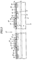
- the image pick-up device generally comprises a semiconductor substrate 10, a sensing and vertical transfer section 20 and a horizontal charge transfer section 30.
- the semiconductor substrate 10 is constituted of a base substrate 12, a first region 14 and a second region 16 (Fig. 2).
- the base substrate 12 is formed of N-type semiconductor. More practically, the base substrate 12 is N-type silicon substrate.
- the first region 14 is formed by P-type layer which is deposited on the N-type silicon substrate.
- the second layer is formed by P ⁇ -type or N ⁇ -type layer and deposited on the first region 14.
- the first and second regions are deposited on the base substrate 12 by epitaxial growth.
- the surface of the second region 16 serves as a primary surface 18 of the semiconductor substrate 10 by selective diffusion or ion implantation.
- the sensing and vertical transfer section 20 includes a plurality of photo-sensing areas 22 and vertical shift registers 24.
- Each of the photo-sensing area 22 serves as a picture element or pixel for receiving the light to produce and store a signal charge therein.
- a given number of photo-sensing areas 22 are arranged in spaced apart relationship to each other and aligned along the associated vertical shift register 24.
- the vertical shift register 24 receives signal charge from the associated photo-sensing areas and vertically transfers the signal charge at every period corresponding to the horizontal blanking period.
- Each of the shift registers 24 and the associated photo-sensing areas 22 constitute a vertical transfer portion 25.
- the vertical shift registers 24 are associated with a horizontal shift register 32 in the horizontal charge transfer section 30 to output the signal charge therethrough to an output section 34.
- an inner channel stop region 40 are formed surrounding the aforementioned sensing and vertical transfer section 20.
- This inner channel stop region 40 is a low impurity concentration region formed by doping impurity, such as boron B.
- the inner channel stop region 40 is formed by doping boron as impurity in the order of 1012 atoms/cm3 by diffusion or ion implantation.
- the inner channel stop region 40 is connected to an outer channel stop region 42 at both ends thereof through bridging section 44.
- the outer channel stop region 42 comprises an inner low impurity concentration region 46 and an outer high impurity concentration region 48.
- the low impurity concentration region 46 of the outer channel stop region 42 has the identical composition to that of the inner channel stop region 40 and preferably formed simultaneously to formation of the inner channel stop region.
- the high impurity concentration region 48 has higher impurity concentration than that in the inner channel stop region.
- the high impurity concentration region 48 is formed by doping impurity, such as boron B,in the order of 1014 atoms/cm2.
- the high impurity concentration region 48 is formed in advance of formation of the inner channel stop region 40 and the low impurity concentration region 46.
- the high impurity concentration region 48 is formed with a plurality of contacting points 50 through which it contact with A1 wiring 52. These contacting points 50 have applied to them a potential at the ground level or a predetermined level, through the wiring 52. Therefore, the contact points 50 serves as a terminal section.
- a resistor region 54 is formed between the inner channel stop region 40 at the low impurity concentration region 46 of the outer channel stop region 42. Namely, the resistor region 54 is formed in a space defined by the inner channel stop region 40, the low impurity concentration region 46 and the bridging section 44. In the preferred construction, the resistor region 54 is formed of a meshed structure. By forming the resistor region 54 in the meshed structure, influence of damaging of part of the resistor region 54 can be eliminated or reduced.
- the base substrate 12 is formed of N-type semiconductor substrate.
- the first region 14 is formed into P+-type region by doping P+-type impurity and the second region 16 is formed into N ⁇ -type region by doping N ⁇ -type impurity.
- Each photo-sensing area 22 is formed in the second region 16 by doping N+-type impurity by selective diffusion or ion implantation, in a predetermined area and through a given depth in conjunction with the primary surface 18 of the semiconductor substrate 10.
- the upper surface of each photo-sensing area 22 is covered by a mutually separate, independent surface region 26.
- the surface regions 26 are electrically conductive.
- each of the surface regions 26 are formed by doping P+-type impurity by way of selective diffusion or ion implantation, in a predetermined area and substantially thin given depth.
- the surface regions 26 are exposed to the primary surface 18 of the semiconductor substrate 10. Forming the surface region 26 will successfully eliminate noise to be created by influence of defects in the crystal structure at the surface area of the semiconductor substrate 10.
- the shift register 24 comprises a vertical charge transfer region 28 formed on the primary surface 18 of the semiconductor substrate 10.
- the vertical charge transfer region 28 is also formed by doping N+-type impurity by way of selective diffusion or ion implantation, similarly to the photo-sensing areas 22.
- the primary surface 18 of the semiconductor substrate 10 is coated by an insulating layer 60.
- the insulating layer may comprise a SiO2 layer.
- a surface electrode 62 is formed over the insulating layer 60.
- the surface electrode 62 is formed of a transparent material for passing the light.
- a given fixed potential is applied to the sensing and vertically transfer section 20 through the surface electrode 62.
- Transfer electrodes 64 are provided, to which a two-phase clock voltage for the vertical shift register 24, is applied.
- the transfer electrodes 64 also serve as transfer gate electrodes for transferring the signal charge of respectively associated photo-sensing sreas 22 to the corresponding charge transfer region 28.
- each of the transfer electrodes 63 is disposed within the insulating layer 60 and thus electrically insulated from surface electrode 62.
- the surface electrode 62 and the transfer electrodes 64 are formed of a silicon monocrystalline dopped impurity to provide low specific contact resistance.
- the channel stop regions 40 and 42 are also formed in the second region 16. As will be seen from Fig. 2, the inner channel stop region 40 and the low impurity concentration region 44 of the outer channel stop region 42 are formed by doping P ⁇ -type impurity at low rate. The inner channel stop region 40 adjoins with the adjacent photo-sensing areas 22 and the surface regions 26. The high impurity concentration region 46 are formed by doping P-type impurity at high rate. A P-type region (not shown) is formed through the second region 16 to establish electric communication between the high impurity concentration region 46 and the first region 14 of the semiconductor substrate 10.
- a given positive voltage e.g. 10V is applied to the base substrate 10 to enable the operation of the image pick-up device. Electrons are thus generated in each photo-sensing area 22. The number of electrons generated in the photo-sensing area 22 will be determined corresponding to the amount of the light received.
- the excessive carriers i.e. the overflown electrons are absorbed in the base substrate 12 which serves as an overflow drain.
- the other carrier e.g. the holes, are drained through the inner channel stop region 40.
- the inner channel stop region 40 is connected to the terminal section 50 through high resistance registor region 54, to be connected to the ground or power supply, the potential at every sections of the inner channel stop region 40 becomes substantially uniform.
- the distance between each individual photo-sensing area 22 and the inner channel stop region 40 can not influence to carrier absorbing characteristics of each section of the inner channel region 40. This allows the depth of the potential well in the photo-sensing areas 22 and thus the handling charge in respective photo-sensing area to be rendered uniform.
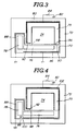
- Fig. 3 shows another embodiment of the image pick-up device according to the invention.
- a P+-type region 70 is formed between N-type base substrate and N ⁇ - type surface layer of the N-type semiconductor substrate 72, in substantially similar manner to that illustrated in Fig. 2.
- the P+-type region 70 is formed by exitaxial growth on the N-type base substrate.
- a sensing and vertically transfer section 74 is formed on the aforementioned N ⁇ -type surface layer at the position approximately corresponding to the center of the P+-type region 70.
- the structure of the sensing and vertical transfer section 74 is substantially the same as that illustrated in Figs. 1 and 2 and thus does not described in detail in order to avoid redundant recitation.
- a horizontal shift register 76 is also formed within the well region 70 and located adjacent the aforementioned sensing and vertical transfer section 74. Adjacent one end of the horizontal shift register 76, an output section 78 is formed. The output section 78 is located away from the sensing and vertically transfer section 74. A channel stop region 75 is formed along the boundary of the sensing and vertical transfer section 74.
- one component of the carriers e.g. electrons are drained to the N-type base substrate via the P+-type region 70 and the other carrier component, e.g. holes, are drained to the channel stop region 75.
- a first grounding wiring 80 is also formed on the N ⁇ -type surface layer and located in an area corresponding to the P+-type region 70.
- the grounding wiring 80 is arranged on the channel stop region 75 and connected thereto.
- the first grounding wiring 80 substantially surrounds the sensing and vertical transfer section 74 with leaving one edge of the sensing and vertical transfer section 74 open, which edge opposes to the horizontal shift register.
- the grounding wiring 80 is connected to the ground level 82 through a resistor 84.
- a second grounding wiring 86 is further formed on the N ⁇ -type surface layer adjacent the horizontal shift register 76. As shown in Fig. 3, the second grounding wiring 86 extends substantially along the longer edge at the side remote from the sensing and vertical transfer section 74 and along the shorter edge at the side remote from the output section 78. This second grounding wiring 86 is directly connected to the ground level.
- a third grounding wiring 88 is formed on the surface layer of the semiconductor substrate adjacent the output section 78.
- the third grounding wiring substantially surrounding the output section 78 with leaving an edge portion opposing one edge of the horizontal shift register open.
- the third grounding wiring is directly connected to the ground level.
- the P+-type region 70 is formed on the semiconductor substrate with providing portions 90 and 92 where the P+-type layer is not deposited and is the bear N-type substrate.
- the portion 90 is located between ends of the first and second grounding wirings 80 and 86 to define a high resistance region 96.
- the portion 92 is located between the first and third grounding wirings 80 and 88 to define therebetween a high resistance region 98.
- respective first, second and third grounding wirings 80, 86 and 88 are separated to each other by the high resistance regions 96 and 98 defined therebetween. Therefore, the potentials at the second and third grounding wirings 86 and 88 which are directly connected to the ground level, will never influence to the sensing and vertical transfer section 74.
- the shown embodiment provides the high resistance regions 96 and 98 by providing the portions 90 and 92, it would be possible to form such high resistance regions by reducing the depth of the channel stop region to provide high resistance. Also it would be possible to form a substantially high resistance region or insulating region by dopping suitable impurity by way of ion implantation in order to reduce conductivity.
- the resistor 84 can be formed on the semiconductor substrate 72 or can be interposed between the ground level 82 and the grounding wiring 80 as an external accessory.
- the potential at the sensing and vertical transfer section is provided at different level to the ground level. This isolates the sensing and vertical transfer section from the directly grounded grounding wirings.
- the potential becomes different at respective portions in the sensing and vertical transfer section 74, because of difference of distance to the grounding wiring.
- the potential difference at respective portions in the sensing and vertical transfer section can be relatively small to be ignored. Therefore, by adjusting the resistance in the high resistance region and the resistor, the potential in each portion of the sensing and vertically transfer section can be held uniform. Therefore, handling charge in each of the photo-sensing areas in the sensing and vertically transfer section become substantially uniform.
- the required combined resistance for maintaining the potential at every portions of the sensing and vertical transfer section uniform will be different depending upon the size of the sensing and vertical transfer section, capacity Cox of the oxide layer of gate electrode, level of the pulse to be applied to the electrode, and so forth.
- the combined resistance may be set in a range of 10 to 100 ⁇ .
- Fig. 4 shows a modification of the aforementioned another embodiment of the image pick-up device of Fig. 3.
- the first and second grounding wirings in the former embodiment are integrally formed to constitute a single grounding wiring 102.
- the grounding wiring 102 is connected to the ground level through a resistor 84. This grounding wire 102 is disconnected from the third grounding wiring 88 which is directly connected to the ground level by the portions 92 and 94 defining the high resistance regions 98 and 100.
- the potential at every portion of the sensing and vertical transfer section 74 can be maintained uniform by adjusting combined resistance of the high resistance regions 98 and 100 and the resistor 84. Therefore, handling charge in each photo-sensing areas in the sensing and vertical transfer section 74 become substantially uniform.
Landscapes
- Engineering & Computer Science (AREA)
- Power Engineering (AREA)
- Physics & Mathematics (AREA)
- Computer Hardware Design (AREA)
- General Physics & Mathematics (AREA)
- Condensed Matter Physics & Semiconductors (AREA)
- Electromagnetism (AREA)
- Microelectronics & Electronic Packaging (AREA)
- Multimedia (AREA)
- Signal Processing (AREA)
- Solid State Image Pick-Up Elements (AREA)
- Transforming Light Signals Into Electric Signals (AREA)
- Element Separation (AREA)
Applications Claiming Priority (4)
| Application Number | Priority Date | Filing Date | Title |
|---|---|---|---|
| JP61061785A JPH0763090B2 (ja) | 1986-03-19 | 1986-03-19 | 固体撮像装置 |
| JP6178586 | 1986-03-19 | ||
| JP61785/86 | 1986-03-19 | ||
| EP87302385A EP0238343B1 (de) | 1986-03-19 | 1987-03-19 | Festkörperabbildungsgerät |
Related Parent Applications (2)
| Application Number | Title | Priority Date | Filing Date |
|---|---|---|---|
| EP87302385A Division EP0238343B1 (de) | 1986-03-19 | 1987-03-19 | Festkörperabbildungsgerät |
| EP87302385.7 Division | 1987-03-19 |
Publications (3)
| Publication Number | Publication Date |
|---|---|
| EP0594559A2 true EP0594559A2 (de) | 1994-04-27 |
| EP0594559A3 EP0594559A3 (en) | 1995-10-25 |
| EP0594559B1 EP0594559B1 (de) | 2001-11-14 |
Family
ID=13181087
Family Applications (2)
| Application Number | Title | Priority Date | Filing Date |
|---|---|---|---|
| EP87302385A Expired - Lifetime EP0238343B1 (de) | 1986-03-19 | 1987-03-19 | Festkörperabbildungsgerät |
| EP94101121A Expired - Lifetime EP0594559B1 (de) | 1986-03-19 | 1987-03-19 | Festkörperabbildungsgerät |
Family Applications Before (1)
| Application Number | Title | Priority Date | Filing Date |
|---|---|---|---|
| EP87302385A Expired - Lifetime EP0238343B1 (de) | 1986-03-19 | 1987-03-19 | Festkörperabbildungsgerät |
Country Status (8)
| Country | Link |
|---|---|
| US (1) | US4780765A (de) |
| EP (2) | EP0238343B1 (de) |
| JP (1) | JPH0763090B2 (de) |
| KR (1) | KR950014688B1 (de) |
| CN (1) | CN1010073B (de) |
| CA (1) | CA1270555A (de) |
| DE (2) | DE3752341T2 (de) |
| HK (1) | HK1007852A1 (de) |
Cited By (2)
| Publication number | Priority date | Publication date | Assignee | Title |
|---|---|---|---|---|
| EP1855321A2 (de) * | 1996-11-01 | 2007-11-14 | The Regents of the University of California | Photonentransparentes Fenster mit niedrigem spezifischem Widerstand an einem lichtempfindlichen Siliciumdetektor |
| US7460010B2 (en) | 2002-11-13 | 2008-12-02 | Carl Freudenberg Kg | System for detecting the rotational motion of a shaft |
Families Citing this family (4)
| Publication number | Priority date | Publication date | Assignee | Title |
|---|---|---|---|---|
| US4928003A (en) * | 1988-07-15 | 1990-05-22 | Tektronix, Inc. | Charge-coupled device for detecting spatial variation in the intensity of electromagnetic radiation |
| US5122850A (en) * | 1989-09-05 | 1992-06-16 | Eastman Kodak Company | Blooming control and reduced image lag in interline transfer CCD area image sensors |
| JPH07177427A (ja) * | 1993-12-20 | 1995-07-14 | Victor Co Of Japan Ltd | ビデオカメラ |
| SG70128A1 (en) * | 1997-10-06 | 2000-01-25 | Canon Kk | Method of driving image sensor |
Citations (5)
| Publication number | Priority date | Publication date | Assignee | Title |
|---|---|---|---|---|
| DE3328607A1 (de) * | 1982-08-11 | 1984-02-16 | Sony Corp., Tokyo | Festkoerper-bildwandler |
| JPS59191378A (ja) * | 1983-04-14 | 1984-10-30 | Sony Corp | 固体撮像素子の製法 |
| JPS59197168A (ja) * | 1983-04-22 | 1984-11-08 | Sony Corp | 固体撮像素子 |
| JPS6118172A (ja) * | 1984-07-04 | 1986-01-27 | Sony Corp | 固体撮像装置 |
| EP0174133A2 (de) * | 1984-08-27 | 1986-03-12 | Sharp Kabushiki Kaisha | Festkörper-Bildsensor |
Family Cites Families (4)
| Publication number | Priority date | Publication date | Assignee | Title |
|---|---|---|---|---|
| JPS56160081A (en) * | 1980-05-14 | 1981-12-09 | Matsushita Electronics Corp | Solid state image pickup apparatus |
| US4593303A (en) * | 1981-07-10 | 1986-06-03 | Fairchild Camera & Instrument Corporation | Self-aligned antiblooming structure for charge-coupled devices |
| US4579626A (en) * | 1985-02-28 | 1986-04-01 | Rca Corporation | Method of making a charge-coupled device imager |
| US4654683A (en) * | 1985-08-23 | 1987-03-31 | Eastman Kodak Company | Blooming control in CCD image sensors |
-
1986
- 1986-03-19 JP JP61061785A patent/JPH0763090B2/ja not_active Expired - Lifetime
-
1987
- 1987-03-13 US US07/025,634 patent/US4780765A/en not_active Expired - Lifetime
- 1987-03-17 KR KR1019870002387A patent/KR950014688B1/ko not_active IP Right Cessation
- 1987-03-18 CA CA000532333A patent/CA1270555A/en not_active Expired - Lifetime
- 1987-03-19 EP EP87302385A patent/EP0238343B1/de not_active Expired - Lifetime
- 1987-03-19 CN CN87102223A patent/CN1010073B/zh not_active Expired
- 1987-03-19 DE DE3752341T patent/DE3752341T2/de not_active Expired - Lifetime
- 1987-03-19 EP EP94101121A patent/EP0594559B1/de not_active Expired - Lifetime
- 1987-03-19 DE DE3751097T patent/DE3751097T2/de not_active Expired - Lifetime
-
1998
- 1998-06-26 HK HK98107003A patent/HK1007852A1/xx not_active IP Right Cessation
Patent Citations (5)
| Publication number | Priority date | Publication date | Assignee | Title |
|---|---|---|---|---|
| DE3328607A1 (de) * | 1982-08-11 | 1984-02-16 | Sony Corp., Tokyo | Festkoerper-bildwandler |
| JPS59191378A (ja) * | 1983-04-14 | 1984-10-30 | Sony Corp | 固体撮像素子の製法 |
| JPS59197168A (ja) * | 1983-04-22 | 1984-11-08 | Sony Corp | 固体撮像素子 |
| JPS6118172A (ja) * | 1984-07-04 | 1986-01-27 | Sony Corp | 固体撮像装置 |
| EP0174133A2 (de) * | 1984-08-27 | 1986-03-12 | Sharp Kabushiki Kaisha | Festkörper-Bildsensor |
Non-Patent Citations (3)
| Title |
|---|
| PATENT ABSTRACTS OF JAPAN vol. 10 no. 168 (E-411) ,14 June 1986 & JP-A-61 018172 (SONY K.K.) 27 January 1986, * |
| PATENT ABSTRACTS OF JAPAN vol. 9 no. 53 (E-301) ,7 March 1985 & JP-A-59 191378 (SONY K.K.) 30 October 1984, * |
| PATENT ABSTRACTS OF JAPAN vol. 9 no. 56 (E-302) ,12 March 1985 & JP-A-59 197168 (SONY K.K.) 8 November 1984, * |
Cited By (3)
| Publication number | Priority date | Publication date | Assignee | Title |
|---|---|---|---|---|
| EP1855321A2 (de) * | 1996-11-01 | 2007-11-14 | The Regents of the University of California | Photonentransparentes Fenster mit niedrigem spezifischem Widerstand an einem lichtempfindlichen Siliciumdetektor |
| EP1855321A3 (de) * | 1996-11-01 | 2008-08-06 | The Regents of the University of California | Rückbeleuchteter und vollständig verarmter CCD mit einer transparenten Fensterschicht mit geringem eletrischem Widerstand |
| US7460010B2 (en) | 2002-11-13 | 2008-12-02 | Carl Freudenberg Kg | System for detecting the rotational motion of a shaft |
Also Published As
| Publication number | Publication date |
|---|---|
| DE3751097T2 (de) | 1995-06-22 |
| EP0238343B1 (de) | 1995-03-01 |
| JPS62219565A (ja) | 1987-09-26 |
| DE3751097D1 (de) | 1995-04-06 |
| EP0594559A3 (en) | 1995-10-25 |
| DE3752341D1 (de) | 2001-12-20 |
| KR870009483A (ko) | 1987-10-27 |
| CA1270555C (en) | 1990-06-19 |
| DE3752341T2 (de) | 2002-07-11 |
| US4780765A (en) | 1988-10-25 |
| HK1007852A1 (en) | 1999-04-23 |
| EP0594559B1 (de) | 2001-11-14 |
| JPH0763090B2 (ja) | 1995-07-05 |
| KR950014688B1 (ko) | 1995-12-13 |
| CN1010073B (zh) | 1990-10-17 |
| CA1270555A (en) | 1990-06-19 |
| EP0238343A2 (de) | 1987-09-23 |
| EP0238343A3 (en) | 1988-10-05 |
| CN87102223A (zh) | 1987-09-30 |
Similar Documents
| Publication | Publication Date | Title |
|---|---|---|
| US4460912A (en) | Solid state image sensors | |
| KR100192954B1 (ko) | 수직형 전달게이트를 가지는 전하결합형 고체촬상소자 및 그 제조방법 | |
| EP0048480B1 (de) | Halbleitender lichtelektrischer Wandler | |
| US8183657B2 (en) | Solid state imaging device comprising charge retention region and buried layer below gate | |
| US4697200A (en) | Field storage drive in interline transfer CCD image sensor | |
| GB2069759A (en) | Anti-blooming in solid-state pick-up cameras | |
| US5416345A (en) | Solid-state image sensor with dark-current eliminator | |
| US20230005981A1 (en) | Solid-state image sensor and electronic device | |
| EP0086845B1 (de) | Halbleiter-bildaufnahmevorrichtung | |
| US5426317A (en) | Frame interline transfer CCD imager | |
| EP0238343B1 (de) | Festkörperabbildungsgerät | |
| US4974043A (en) | Solid-state image sensor | |
| US5990503A (en) | Selectable resolution CCD sensor | |
| KR19980018911A (ko) | 고정된 패턴 잡음 감소 및 스미어 방지 가능한 고체 이미지 픽업 장치 (Solid-State Image Pickup Device Capable of Reducing Fixed Pattern Noise and Preventing Smer) | |
| KR20010021375A (ko) | 고체 촬상 소자 및 그 제조 방법 | |
| US5502319A (en) | Solid state image sensor with non-parallel conductors | |
| US5856846A (en) | Charge-coupled imaging device having electrical connections on the readout register side | |
| JPH04502234A (ja) | 固体撮像器 | |
| EP0511683A2 (de) | Schichtförmig aufgebautes Festkörperbildaufnahmegerät | |
| EP0487989A2 (de) | Festkörperbildsensor | |
| US5907356A (en) | Solid-state image pickup device | |
| KR970007895B1 (ko) | 고체촬상장치 및 노광시간제어방법 | |
| JPS5846905B2 (ja) | コタイサツゾウソウチ | |
| US5929471A (en) | Structure and method for CCD sensor stage selection | |
| EP4123691A1 (de) | Festkörperbildgebungselement und elektronische vorrichtung |
Legal Events
| Date | Code | Title | Description |
|---|---|---|---|
| PUAI | Public reference made under article 153(3) epc to a published international application that has entered the european phase |
Free format text: ORIGINAL CODE: 0009012 |
|
| AC | Divisional application: reference to earlier application |
Ref document number: 238343 Country of ref document: EP |
|
| AK | Designated contracting states |
Kind code of ref document: A2 Designated state(s): DE FR GB NL |
|
| PUAL | Search report despatched |
Free format text: ORIGINAL CODE: 0009013 |
|
| AK | Designated contracting states |
Kind code of ref document: A3 Designated state(s): DE FR GB NL |
|
| 17P | Request for examination filed |
Effective date: 19960404 |
|
| 17Q | First examination report despatched |
Effective date: 19980612 |
|
| GRAG | Despatch of communication of intention to grant |
Free format text: ORIGINAL CODE: EPIDOS AGRA |
|
| GRAG | Despatch of communication of intention to grant |
Free format text: ORIGINAL CODE: EPIDOS AGRA |
|
| GRAH | Despatch of communication of intention to grant a patent |
Free format text: ORIGINAL CODE: EPIDOS IGRA |
|
| GRAH | Despatch of communication of intention to grant a patent |
Free format text: ORIGINAL CODE: EPIDOS IGRA |
|
| GRAA | (expected) grant |
Free format text: ORIGINAL CODE: 0009210 |
|
| AC | Divisional application: reference to earlier application |
Ref document number: 238343 Country of ref document: EP |
|
| AK | Designated contracting states |
Kind code of ref document: B1 Designated state(s): DE FR GB NL |
|
| REF | Corresponds to: |
Ref document number: 3752341 Country of ref document: DE Date of ref document: 20011220 |
|
| REG | Reference to a national code |
Ref country code: GB Ref legal event code: IF02 |
|
| PLBE | No opposition filed within time limit |
Free format text: ORIGINAL CODE: 0009261 |
|
| STAA | Information on the status of an ep patent application or granted ep patent |
Free format text: STATUS: NO OPPOSITION FILED WITHIN TIME LIMIT |
|
| 26N | No opposition filed | ||
| PGFP | Annual fee paid to national office [announced via postgrant information from national office to epo] |
Ref country code: NL Payment date: 20060305 Year of fee payment: 20 |
|
| PGFP | Annual fee paid to national office [announced via postgrant information from national office to epo] |
Ref country code: FR Payment date: 20060308 Year of fee payment: 20 |
|
| PGFP | Annual fee paid to national office [announced via postgrant information from national office to epo] |
Ref country code: GB Payment date: 20060315 Year of fee payment: 20 |
|
| PGFP | Annual fee paid to national office [announced via postgrant information from national office to epo] |
Ref country code: DE Payment date: 20060316 Year of fee payment: 20 |
|
| PG25 | Lapsed in a contracting state [announced via postgrant information from national office to epo] |
Ref country code: GB Free format text: LAPSE BECAUSE OF EXPIRATION OF PROTECTION Effective date: 20070318 |
|
| PG25 | Lapsed in a contracting state [announced via postgrant information from national office to epo] |
Ref country code: NL Free format text: LAPSE BECAUSE OF EXPIRATION OF PROTECTION Effective date: 20070319 |
|
| REG | Reference to a national code |
Ref country code: GB Ref legal event code: PE20 |
|
| NLV7 | Nl: ceased due to reaching the maximum lifetime of a patent |
Effective date: 20070319 |