EP0594340B1 - Method for forming a bipolar transistor - Google Patents
Method for forming a bipolar transistor Download PDFInfo
- Publication number
- EP0594340B1 EP0594340B1 EP93308133A EP93308133A EP0594340B1 EP 0594340 B1 EP0594340 B1 EP 0594340B1 EP 93308133 A EP93308133 A EP 93308133A EP 93308133 A EP93308133 A EP 93308133A EP 0594340 B1 EP0594340 B1 EP 0594340B1
- Authority
- EP
- European Patent Office
- Prior art keywords
- layer
- dopant
- substrate
- region
- spin
- Prior art date
- Legal status (The legal status is an assumption and is not a legal conclusion. Google has not performed a legal analysis and makes no representation as to the accuracy of the status listed.)
- Expired - Lifetime
Links
- 238000000034 method Methods 0.000 title claims description 27
- 239000002019 doping agent Substances 0.000 claims description 22
- 239000000758 substrate Substances 0.000 claims description 14
- OAICVXFJPJFONN-UHFFFAOYSA-N Phosphorus Chemical group [P] OAICVXFJPJFONN-UHFFFAOYSA-N 0.000 claims description 8
- 239000011521 glass Substances 0.000 claims description 8
- 229910052698 phosphorus Inorganic materials 0.000 claims description 8
- 239000011574 phosphorus Substances 0.000 claims description 8
- 239000004065 semiconductor Substances 0.000 claims description 8
- 238000010438 heat treatment Methods 0.000 claims description 7
- ZOXJGFHDIHLPTG-UHFFFAOYSA-N Boron Chemical group [B] ZOXJGFHDIHLPTG-UHFFFAOYSA-N 0.000 claims description 6
- 229910052796 boron Inorganic materials 0.000 claims description 6
- 229910052785 arsenic Inorganic materials 0.000 claims description 3
- RQNWIZPPADIBDY-UHFFFAOYSA-N arsenic atom Chemical compound [As] RQNWIZPPADIBDY-UHFFFAOYSA-N 0.000 claims description 3
- 238000009792 diffusion process Methods 0.000 claims description 3
- PCHJSUWPFVWCPO-UHFFFAOYSA-N gold Chemical compound [Au] PCHJSUWPFVWCPO-UHFFFAOYSA-N 0.000 claims description 3
- 229910052737 gold Inorganic materials 0.000 claims description 3
- 239000010931 gold Substances 0.000 claims description 3
- 229910052751 metal Inorganic materials 0.000 claims description 3
- 239000002184 metal Substances 0.000 claims description 3
- 238000009987 spinning Methods 0.000 claims description 2
- 238000000151 deposition Methods 0.000 claims 1
- 230000015572 biosynthetic process Effects 0.000 description 6
- 239000013078 crystal Substances 0.000 description 6
- XUIMIQQOPSSXEZ-UHFFFAOYSA-N Silicon Chemical compound [Si] XUIMIQQOPSSXEZ-UHFFFAOYSA-N 0.000 description 4
- 239000007943 implant Substances 0.000 description 4
- 239000012535 impurity Substances 0.000 description 4
- 230000007547 defect Effects 0.000 description 3
- 229920000642 polymer Polymers 0.000 description 3
- VYPSYNLAJGMNEJ-UHFFFAOYSA-N Silicium dioxide Chemical compound O=[Si]=O VYPSYNLAJGMNEJ-UHFFFAOYSA-N 0.000 description 2
- 239000012212 insulator Substances 0.000 description 2
- 229920002120 photoresistant polymer Polymers 0.000 description 2
- 229910052710 silicon Inorganic materials 0.000 description 2
- 239000010703 silicon Substances 0.000 description 2
- 229910052787 antimony Inorganic materials 0.000 description 1
- WATWJIUSRGPENY-UHFFFAOYSA-N antimony atom Chemical compound [Sb] WATWJIUSRGPENY-UHFFFAOYSA-N 0.000 description 1
- 230000003247 decreasing effect Effects 0.000 description 1
- 238000011161 development Methods 0.000 description 1
- 230000018109 developmental process Effects 0.000 description 1
- 238000010586 diagram Methods 0.000 description 1
- 238000005516 engineering process Methods 0.000 description 1
- 239000007788 liquid Substances 0.000 description 1
- 230000000873 masking effect Effects 0.000 description 1
- 239000000203 mixture Substances 0.000 description 1
- 239000002245 particle Substances 0.000 description 1
- 230000006798 recombination Effects 0.000 description 1
- 238000005215 recombination Methods 0.000 description 1
- 235000012239 silicon dioxide Nutrition 0.000 description 1
- 239000000377 silicon dioxide Substances 0.000 description 1
- LIVNPJMFVYWSIS-UHFFFAOYSA-N silicon monoxide Chemical class [Si-]#[O+] LIVNPJMFVYWSIS-UHFFFAOYSA-N 0.000 description 1
- 229910052814 silicon oxide Inorganic materials 0.000 description 1
Images

Classifications
-
- H—ELECTRICITY
- H01—ELECTRIC ELEMENTS
- H01L—SEMICONDUCTOR DEVICES NOT COVERED BY CLASS H10
- H01L29/00—Semiconductor devices adapted for rectifying, amplifying, oscillating or switching, or capacitors or resistors with at least one potential-jump barrier or surface barrier, e.g. PN junction depletion layer or carrier concentration layer; Details of semiconductor bodies or of electrodes thereof ; Multistep manufacturing processes therefor
- H01L29/66—Types of semiconductor device ; Multistep manufacturing processes therefor
- H01L29/66007—Multistep manufacturing processes
- H01L29/66075—Multistep manufacturing processes of devices having semiconductor bodies comprising group 14 or group 13/15 materials
- H01L29/66227—Multistep manufacturing processes of devices having semiconductor bodies comprising group 14 or group 13/15 materials the devices being controllable only by the electric current supplied or the electric potential applied, to an electrode which does not carry the current to be rectified, amplified or switched, e.g. three-terminal devices
- H01L29/66234—Bipolar junction transistors [BJT]
- H01L29/66272—Silicon vertical transistors
-
- H—ELECTRICITY
- H01—ELECTRIC ELEMENTS
- H01L—SEMICONDUCTOR DEVICES NOT COVERED BY CLASS H10
- H01L21/00—Processes or apparatus adapted for the manufacture or treatment of semiconductor or solid state devices or of parts thereof
- H01L21/02—Manufacture or treatment of semiconductor devices or of parts thereof
- H01L21/04—Manufacture or treatment of semiconductor devices or of parts thereof the devices having at least one potential-jump barrier or surface barrier, e.g. PN junction, depletion layer or carrier concentration layer
- H01L21/18—Manufacture or treatment of semiconductor devices or of parts thereof the devices having at least one potential-jump barrier or surface barrier, e.g. PN junction, depletion layer or carrier concentration layer the devices having semiconductor bodies comprising elements of Group IV of the Periodic System or AIIIBV compounds with or without impurities, e.g. doping materials
- H01L21/22—Diffusion of impurity materials, e.g. doping materials, electrode materials, into or out of a semiconductor body, or between semiconductor regions; Interactions between two or more impurities; Redistribution of impurities
- H01L21/225—Diffusion of impurity materials, e.g. doping materials, electrode materials, into or out of a semiconductor body, or between semiconductor regions; Interactions between two or more impurities; Redistribution of impurities using diffusion into or out of a solid from or into a solid phase, e.g. a doped oxide layer
- H01L21/2251—Diffusion into or out of group IV semiconductors
- H01L21/2254—Diffusion into or out of group IV semiconductors from or through or into an applied layer, e.g. photoresist, nitrides
- H01L21/2255—Diffusion into or out of group IV semiconductors from or through or into an applied layer, e.g. photoresist, nitrides the applied layer comprising oxides only, e.g. P2O5, PSG, H3BO3, doped oxides
Definitions
- the present invention relates to methods of producing integrated circuit devices and more specifically to a method of forming a bipolar transistor.
- CMOS transistors typically formed using bipolar transistors.
- CMOS transistors typically made of silicon.
- the base is formed with the first mask, etch, and implant operation.
- the photoresist layer used during the masking operation is removed and a new photoresist layer is provided before the second implanting operation.
- the emitter is formed during the second mask, etch, and implant operation. In such a process, the implant energy has to be reduced to produce shallow junctions.
- This method suffers from the disadvantage that implanting produces defects which lie in the space charge region of the junction.
- the implanted impurity is brought to rest by an inelastic collision with silicon atoms in the crystal lattice, which damages the crystal lattice structure by knocking silicon atoms out of place.
- the crystal lattice structure must be epitaxially regrown by a thermal anneal to activate the implanted impurities by incorporating them into the crystal lattice.
- a rapid thermal process (RTP) cycle is typically performed.
- the damage from implanting is not totally repairable without causing undesirable enhanced diffusion of the impurities which is inconsistent with shallow junction technology. Defect sites having energies in the middle of the band gap remain and produce a conduction path which ultimately causes a leakage current to flow.
- a method of forming a semiconductor device comprising the steps of:
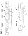
- Transistor 10 includes underlying collector layer 12, base layer 14, emitter layer 16, field oxide portions 18, insulating layer 20, and metal interconnect layer 22.
- collector 12 and field oxide portions 18 are defined using known BiCMOS or bipolar process steps.
- layer 33 of doped SOG is spun onto collector 12 at a thickness anywhere between about 10 nm to 15 micrometers, with a preferred thickness of about 300 to 500 nm.
- Layer 33 preferably includes two dopants, such as boron and phosphorus.
- a base dopant is chosen which will diffuse faster than the emitter dopant at a predetermined temperature.
- boron is used to form base 14 while phosphorus is used to form emitter 16.
- Other dopants may include arsenic, antimony, and gold.
- Arsenic may be used in place of phosphorus to provide more abrupt junctions.
- Gold may be combined with phosphorus to increase the generation or recombination rate of electrons, thus allowing device 10 to operate at higher frequencies.
- a first way is to put the dopant into the SOG polymer.
- a second way is to leave the dopant as a free-floating particle suspended outside the polymer.
- concentrations of about 4% boron and about 1% phosphorus have worked well.
- the base and emitter dopants are both driven into collector 12 using a single rapid thermal process (RTP) cycle.
- RTP rapid thermal process
- the substrate is heated to about 1050 degrees Celsius for about 60 seconds.
- the substrate is heated to about 1100 degrees Celsius for about 40 seconds.
- the described method enables the formation of devices having shallow and abrupt junctions, without damage to the crystal lattice of the silicon.
- the width of base 14 may be varied by varying the heating time or temperature. Relatively speaking, smaller base widths can be produced by either lowering the temperature or decreasing the heating time.
- layer 33 is changed to silicon dioxide, which is an insulator.
- layer 33 may be left in place or removed by a plasma or wet etch process in favour of a better insulator. Undoped silicon oxides are preferred.
- a portion of layer 20 over emitter 16 is removed by a mask and etch operation (Fig. 3).
- boron is implanted into the exposed portion of emitter 16. This step is performed to provide a contact point for base 14 (Fig. 4).
- metal interconnect layer 22 is deposited over layer 20.
- the described method enables the formation of devices having shallow and abrupt junctions, without causing damage to the crystal lattice structure.
Description
- The present invention relates to methods of producing integrated circuit devices and more specifically to a method of forming a bipolar transistor.
- Known methods for forming bipolar transistors involve at least two mask, etch, and implant operations in which n-type and p-type impurities are implanted into a collector, typically made of silicon. The base is formed with the first mask, etch, and implant operation. The photoresist layer used during the masking operation is removed and a new photoresist layer is provided before the second implanting operation. The emitter is formed during the second mask, etch, and implant operation. In such a process, the implant energy has to be reduced to produce shallow junctions.
- This method suffers from the disadvantage that implanting produces defects which lie in the space charge region of the junction. The implanted impurity is brought to rest by an inelastic collision with silicon atoms in the crystal lattice, which damages the crystal lattice structure by knocking silicon atoms out of place. The crystal lattice structure must be epitaxially regrown by a thermal anneal to activate the implanted impurities by incorporating them into the crystal lattice. For shallow junctions, a rapid thermal process (RTP) cycle is typically performed. The damage from implanting is not totally repairable without causing undesirable enhanced diffusion of the impurities which is inconsistent with shallow junction technology. Defect sites having energies in the middle of the band gap remain and produce a conduction path which ultimately causes a leakage current to flow.
- The document Motorola Technical Developments, Volume 4, April 1984, pages 32-33 discloses a method of achieving so-called one-step transistor formation utilising a liquid source containing a mixture of n-type and p-type dopants which is spun on a semiconductor wafer, baked, and so diffused into the substrate.
- It is an object of the present invention to provide a simple method for forming a semiconductor device wherein the disadvantages caused by defect sites are alleviated.
- Therefore, according to the present invention, there is provided a method of forming a semiconductor device, comprising the steps of:
- spinning a layer of spin on glass over a semiconductor substrate which includes a collector region and wherein the layer of spin on glass includes first and second dopants having different diffusion rates into the semiconductor substrate;
- heating the substrate to drive the dopants simultaneously into the substrate region, and wherein the first dopant forms a base region and the second dopant forms an emitter region and characterised by the steps or removing a portion of the layer spin on glass over said emitter region;
- and implanting the exposed emitter region portion with said first dopant to provide a base contact region.
-
- One embodiment of the present invention will now be described by way of example with reference to the accompanying drawings, in which:-
- Fig. 1 is a cross-sectional view of a bipolar transistor formed using the method of the present invention;
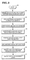
- Fig. 2 is a flow diagram of the method of the present invention;
- Fig. 3 is a cross-sectional view of the bipolar transistor of Fig. 1 at a point in its formation;
- Fig. 4 is a cross-sectional view of the bipolar transistor of Fig. 1 at a point in its formation; and
- Fig. 5 is a cross-sectional view of the bipolar transistor of Fig. 1 at a point in its formation.
-
- Referring now to Fig. 1, a
bipolar transistor 10 manufactured using the method of the present invention is shown.Transistor 10 includesunderlying collector layer 12,base layer 14,emitter layer 16,field oxide portions 18,insulating layer 20, andmetal interconnect layer 22. - Turning now to Fig. 2, the method of the present invention begins at
START 28. Inblock 30,collector 12, andfield oxide portions 18 are defined using known BiCMOS or bipolar process steps. - In
block 32,layer 33 of doped SOG is spun ontocollector 12 at a thickness anywhere between about 10 nm to 15 micrometers, with a preferred thickness of about 300 to 500 nm.Layer 33 preferably includes two dopants, such as boron and phosphorus. A base dopant is chosen which will diffuse faster than the emitter dopant at a predetermined temperature. Preferably, boron is used to formbase 14 while phosphorus is used to formemitter 16. Other dopants may include arsenic, antimony, and gold. Arsenic may be used in place of phosphorus to provide more abrupt junctions. Gold may be combined with phosphorus to increase the generation or recombination rate of electrons, thus allowingdevice 10 to operate at higher frequencies. - There are two different ways of doping the SOG. A first way is to put the dopant into the SOG polymer. A second way is to leave the dopant as a free-floating particle suspended outside the polymer. When boron and phosphorus are part of the polymer, concentrations of about 4% boron and about 1% phosphorus have worked well.
- In
block 34, the base and emitter dopants are both driven intocollector 12 using a single rapid thermal process (RTP) cycle. This involves heating the substrate to a predetermined temperature for a predetermined time. In one example the substrate is heated to about 1050 degrees Celsius for about 60 seconds. In another example the substrate is heated to about 1100 degrees Celsius for about 40 seconds. The described method enables the formation of devices having shallow and abrupt junctions, without damage to the crystal lattice of the silicon. The width ofbase 14 may be varied by varying the heating time or temperature. Relatively speaking, smaller base widths can be produced by either lowering the temperature or decreasing the heating time. During the RTP cycle,layer 33 is changed to silicon dioxide, which is an insulator. - In
block 36,layer 33 may be left in place or removed by a plasma or wet etch process in favour of a better insulator. Undoped silicon oxides are preferred. - In
block 38, a portion oflayer 20 overemitter 16 is removed by a mask and etch operation (Fig. 3). - In
block 40, boron is implanted into the exposed portion ofemitter 16. This step is performed to provide a contact point for base 14 (Fig. 4). - In
block 42, another portion oflayer 20 is removed to provide a contact point foremitter 16. A mask and etch operation is performed (Fig. 5). - In
block 44,metal interconnect layer 22 is deposited overlayer 20. - The described method enables the formation of devices having shallow and abrupt junctions, without causing damage to the crystal lattice structure.
Claims (7)
- A method of forming a semiconductor device, comprising the steps of:spinning a layer of spin on glass (33) over a semiconductor substrate which includes a collector region (12) and wherein the layer of spin on glass (33) includes first and second dopants having different diffusion rates into the semiconductor substrate;heating the substrate to drive the dopants simultaneously into the substrate region (12), and wherein the first dopant forms a base region (14) and the second dopant forms an emitter region (16) and characterised by the steps of removing a portion of the layer of spin on glass (33) over said emitter region (16);and implanting the exposed emitter region portion with said first dopant to provide a base contact region.
- A method according to Claim 1, characterised in that said first dopant is boron and said second dopant is phosphorus or arsenic.
- A method according to Claim 2, characterised in that said second dopant is phosphorus and in that said layer of spin on glass (33) includes a third dopant comprising gold.
- A method according to any one of the preceding claims, characterised in that said step of heating includes heating said substrate for a predetermined time in a rapid thermal process (RTP) cycle.
- A method according to Claim 4, characterised in that said predetermined temperature is about 1050 degrees Celsius and said predetermined time is about 60 seconds.
- A method according to Claim 4, characterised in that said predetermined temperature is about 1100 degrees Celsius and said predetermined time is about 40 seconds.
- A method according to Claim 1, characterised by the steps of removing a further portion of said layer of spin on glass over said emitter region (16), and depositing a metal interconnect layer (22) over said substrate.
Applications Claiming Priority (2)
| Application Number | Priority Date | Filing Date | Title |
|---|---|---|---|
| US965823 | 1992-10-23 | ||
| US07/965,823 US5340752A (en) | 1992-10-23 | 1992-10-23 | Method for forming a bipolar transistor using doped SOG |
Publications (3)
| Publication Number | Publication Date |
|---|---|
| EP0594340A2 EP0594340A2 (en) | 1994-04-27 |
| EP0594340A3 EP0594340A3 (en) | 1996-04-24 |
| EP0594340B1 true EP0594340B1 (en) | 1999-03-24 |
Family
ID=25510546
Family Applications (1)
| Application Number | Title | Priority Date | Filing Date |
|---|---|---|---|
| EP93308133A Expired - Lifetime EP0594340B1 (en) | 1992-10-23 | 1993-10-12 | Method for forming a bipolar transistor |
Country Status (4)
| Country | Link |
|---|---|
| US (1) | US5340752A (en) |
| EP (1) | EP0594340B1 (en) |
| JP (1) | JP3459282B2 (en) |
| DE (1) | DE69324098T2 (en) |
Families Citing this family (4)
| Publication number | Priority date | Publication date | Assignee | Title |
|---|---|---|---|---|
| DE3717639C2 (en) * | 1987-05-26 | 1996-07-11 | Wild Maschinen Gmbh | Transfer press with resilient compensation devices |
| US5994209A (en) * | 1996-11-13 | 1999-11-30 | Applied Materials, Inc. | Methods and apparatus for forming ultra-shallow doped regions using doped silicon oxide films |
| EP0930166B1 (en) * | 1997-10-21 | 2005-02-23 | Microjet Technology Co., Ltd | Manufacturing process and structure of ink jet printhead |
| DE10058031B4 (en) * | 2000-11-23 | 2007-11-22 | Advanced Micro Devices, Inc., Sunnyvale | A method of forming lightly doped halo regions and extension regions in a semiconductor device |
Family Cites Families (30)
| Publication number | Priority date | Publication date | Assignee | Title |
|---|---|---|---|---|
| GB1099049A (en) * | 1965-12-28 | 1968-01-10 | Telefunken Patent | A method of manufacturing transistors |
| US3928225A (en) * | 1971-04-08 | 1975-12-23 | Semikron Gleichrichterbau | Glass forming mixture with boron as the doping material for producing conductivity zones in semiconductor bodies by means of diffusion |
| US3915766A (en) * | 1972-05-31 | 1975-10-28 | Texas Instruments Inc | Composition for use in forming a doped oxide film |
| JPS53135263A (en) * | 1977-04-28 | 1978-11-25 | Nec Corp | Production of semiconductor device |
| US4355454A (en) * | 1979-09-05 | 1982-10-26 | Texas Instruments Incorporated | Coating device with As2 -O3 -SiO2 |
| US4455325A (en) * | 1981-03-16 | 1984-06-19 | Fairchild Camera And Instrument Corporation | Method of inducing flow or densification of phosphosilicate glass for integrated circuits |
| JPS57194525A (en) * | 1981-05-26 | 1982-11-30 | Fujitsu Ltd | Manufacture of semiconductor device |
| US4571366A (en) * | 1982-02-11 | 1986-02-18 | Owens-Illinois, Inc. | Process for forming a doped oxide film and doped semiconductor |
| US4433008A (en) * | 1982-05-11 | 1984-02-21 | Rca Corporation | Doped-oxide diffusion of phosphorus using borophosphosilicate glass |
| JPH0719759B2 (en) * | 1984-09-13 | 1995-03-06 | セイコーエプソン株式会社 | Method for manufacturing semiconductor device |
| JPS6151912A (en) * | 1984-08-22 | 1986-03-14 | Nec Corp | Manufacture of semiconductor device |
| US4606114A (en) * | 1984-08-29 | 1986-08-19 | Texas Instruments Incorporated | Multilevel oxide as diffusion source |
| US4628589A (en) * | 1984-09-28 | 1986-12-16 | Texas Instruments Incorporated | Method for fabricating stacked CMOS structures |
| US4603468A (en) * | 1984-09-28 | 1986-08-05 | Texas Instruments Incorporated | Method for source/drain self-alignment in stacked CMOS |
| JPS6260220A (en) * | 1985-09-09 | 1987-03-16 | Seiko Epson Corp | Manufacture of semiconductor device |
| JPS6273711A (en) * | 1985-09-27 | 1987-04-04 | Nec Corp | Semiconductor device |
| US4661177A (en) * | 1985-10-08 | 1987-04-28 | Varian Associates, Inc. | Method for doping semiconductor wafers by rapid thermal processing of solid planar diffusion sources |
| GB8527062D0 (en) * | 1985-11-02 | 1985-12-04 | Plessey Co Plc | Mos transistor manufacture |
| JPS62216322A (en) * | 1986-03-18 | 1987-09-22 | Fujitsu Ltd | Manufacture of semiconductor device |
| JPS6342120A (en) * | 1986-08-07 | 1988-02-23 | Nec Corp | Manufacture of semiconductor device |
| JPH0748516B2 (en) * | 1986-09-26 | 1995-05-24 | アメリカン テレフォン アンド テレグラフ カムパニー | Method of manufacturing a dielectrically isolated device having a buried conductive layer |
| JPS6459858A (en) * | 1987-08-31 | 1989-03-07 | Toshiba Corp | Manufacture of semiconductor device |
| JPH01123417A (en) * | 1987-11-07 | 1989-05-16 | Mitsubishi Electric Corp | Manufacture of semiconductor device |
| JPH01179357A (en) * | 1988-01-04 | 1989-07-17 | Toshiba Corp | Manufacture of semiconductor device |
| US4891331A (en) * | 1988-01-21 | 1990-01-02 | Oi-Neg Tv Products, Inc. | Method for doping silicon wafers using Al2 O3 /P2 O5 composition |
| JPH0254522A (en) * | 1988-08-18 | 1990-02-23 | Fuji Electric Co Ltd | Impurity diffusion of semiconductor layer |
| US5047357A (en) * | 1989-02-03 | 1991-09-10 | Texas Instruments Incorporated | Method for forming emitters in a BiCMOS process |
| US4910160A (en) * | 1989-06-06 | 1990-03-20 | National Semiconductor Corporation | High voltage complementary NPN/PNP process |
| US5024959A (en) * | 1989-09-25 | 1991-06-18 | Motorola, Inc. | CMOS process using doped glass layer |
| US5322805A (en) * | 1992-10-16 | 1994-06-21 | Ncr Corporation | Method for forming a bipolar emitter using doped SOG |
-
1992
- 1992-10-23 US US07/965,823 patent/US5340752A/en not_active Expired - Fee Related
-
1993
- 1993-10-12 EP EP93308133A patent/EP0594340B1/en not_active Expired - Lifetime
- 1993-10-12 DE DE69324098T patent/DE69324098T2/en not_active Expired - Fee Related
- 1993-10-22 JP JP28627693A patent/JP3459282B2/en not_active Expired - Fee Related
Also Published As
| Publication number | Publication date |
|---|---|
| DE69324098T2 (en) | 1999-08-12 |
| JPH06216146A (en) | 1994-08-05 |
| EP0594340A3 (en) | 1996-04-24 |
| US5340752A (en) | 1994-08-23 |
| EP0594340A2 (en) | 1994-04-27 |
| JP3459282B2 (en) | 2003-10-20 |
| DE69324098D1 (en) | 1999-04-29 |
Similar Documents
| Publication | Publication Date | Title |
|---|---|---|
| US5279976A (en) | Method for fabricating a semiconductor device having a shallow doped region | |
| US5279978A (en) | Process for making BiCMOS device having an SOI substrate | |
| EP0090940B1 (en) | Method of forming emitter and intrinsic base regions of a bipolar transistor | |
| US6475887B1 (en) | Method of manufacturing semiconductor device | |
| US5137840A (en) | Vertical bipolar transistor with recessed epitaxially grown intrinsic base region | |
| EP0715769B1 (en) | Self-aligned cmos process | |
| US5235206A (en) | Vertical bipolar transistor with recessed epitaxially grown intrinsic base region | |
| JPH0147014B2 (en) | ||
| EP0594339B1 (en) | Method of manufacturing a CMOS device | |
| US5453389A (en) | Defect-free bipolar process | |
| US4534806A (en) | Method for manufacturing vertical PNP transistor with shallow emitter | |
| EP0594340B1 (en) | Method for forming a bipolar transistor | |
| EP0166923A2 (en) | High performance bipolar transistor having a lightly doped guard ring disposed between the emitter and the extrinsic base region | |
| US5322805A (en) | Method for forming a bipolar emitter using doped SOG | |
| US20030062589A1 (en) | Method for manufacturing and structure of semiconductor device with shallow trench collector contact region | |
| US6806159B2 (en) | Method for manufacturing a semiconductor device with sinker contact region | |
| US7164186B2 (en) | Structure of semiconductor device with sinker contact region | |
| JPH11274090A (en) | Manufacture of device with shallow junction | |
| JP2527628B2 (en) | Method for manufacturing semiconductor device | |
| EP0042380A4 (en) | Method for achieving ideal impurity base profile in a transistor. | |
| RU2106037C1 (en) | Method for producing vertical p-n-p transistor as part of integrated circuit | |
| KR940004257B1 (en) | Manufacturing method of bipolar transistor | |
| KR0154307B1 (en) | Method of fabricating semiconductor device | |
| JPH0567623A (en) | Manufacture of semiconductor device | |
| KR19980036830A (en) | Bipolar Junction Transistor Manufacturing Method |
Legal Events
| Date | Code | Title | Description |
|---|---|---|---|
| PUAI | Public reference made under article 153(3) epc to a published international application that has entered the european phase |
Free format text: ORIGINAL CODE: 0009012 |
|
| AK | Designated contracting states |
Kind code of ref document: A2 Designated state(s): DE GB |
|
| RAP1 | Party data changed (applicant data changed or rights of an application transferred) |
Owner name: AT&T GLOBAL INFORMATION SOLUTIONS INTERNATIONAL IN |
|
| RAP1 | Party data changed (applicant data changed or rights of an application transferred) |
Owner name: HYUNDAI ELECTRONICS AMERICA Owner name: AT&T GLOBAL INFORMATION SOLUTIONS INTERNATIONAL IN |
|
| PUAL | Search report despatched |
Free format text: ORIGINAL CODE: 0009013 |
|
| AK | Designated contracting states |
Kind code of ref document: A3 Designated state(s): DE GB |
|
| RAP1 | Party data changed (applicant data changed or rights of an application transferred) |
Owner name: SYMBIOS LOGIC INC. Owner name: HYUNDAI ELECTRONICS AMERICA Owner name: AT&T GLOBAL INFORMATION SOLUTIONS INTERNATIONAL IN |
|
| 17P | Request for examination filed |
Effective date: 19960603 |
|
| 17Q | First examination report despatched |
Effective date: 19960812 |
|
| RAP1 | Party data changed (applicant data changed or rights of an application transferred) |
Owner name: SYMBIOS LOGIC INC. Owner name: HYUNDAI ELECTRONICS AMERICA Owner name: NCR INTERNATIONAL, INC. |
|
| RAP1 | Party data changed (applicant data changed or rights of an application transferred) |
Owner name: SYMBIOS, INC. Owner name: HYUNDAI ELECTRONICS AMERICA Owner name: NCR INTERNATIONAL, INC. |
|
| GRAG | Despatch of communication of intention to grant |
Free format text: ORIGINAL CODE: EPIDOS AGRA |
|
| GRAG | Despatch of communication of intention to grant |
Free format text: ORIGINAL CODE: EPIDOS AGRA |
|
| GRAH | Despatch of communication of intention to grant a patent |
Free format text: ORIGINAL CODE: EPIDOS IGRA |
|
| GRAH | Despatch of communication of intention to grant a patent |
Free format text: ORIGINAL CODE: EPIDOS IGRA |
|
| GRAA | (expected) grant |
Free format text: ORIGINAL CODE: 0009210 |
|
| AK | Designated contracting states |
Kind code of ref document: B1 Designated state(s): DE GB |
|
| REF | Corresponds to: |
Ref document number: 69324098 Country of ref document: DE Date of ref document: 19990429 |
|
| PLBE | No opposition filed within time limit |
Free format text: ORIGINAL CODE: 0009261 |
|
| STAA | Information on the status of an ep patent application or granted ep patent |
Free format text: STATUS: NO OPPOSITION FILED WITHIN TIME LIMIT |
|
| 26N | No opposition filed | ||
| REG | Reference to a national code |
Ref country code: GB Ref legal event code: IF02 |
|
| REG | Reference to a national code |
Ref country code: GB Ref legal event code: 732E |
|
| PGFP | Annual fee paid to national office [announced via postgrant information from national office to epo] |
Ref country code: GB Payment date: 20051012 Year of fee payment: 13 |
|
| PGFP | Annual fee paid to national office [announced via postgrant information from national office to epo] |
Ref country code: DE Payment date: 20070430 Year of fee payment: 14 |
|
| GBPC | Gb: european patent ceased through non-payment of renewal fee |
Effective date: 20061012 |
|
| PG25 | Lapsed in a contracting state [announced via postgrant information from national office to epo] |
Ref country code: GB Free format text: LAPSE BECAUSE OF NON-PAYMENT OF DUE FEES Effective date: 20061012 |
|
| PG25 | Lapsed in a contracting state [announced via postgrant information from national office to epo] |
Ref country code: DE Free format text: LAPSE BECAUSE OF NON-PAYMENT OF DUE FEES Effective date: 20080501 |