EP0591723B1 - Elektrische Verbindervorrichtung - Google Patents
Elektrische Verbindervorrichtung Download PDFInfo
- Publication number
- EP0591723B1 EP0591723B1 EP93114805A EP93114805A EP0591723B1 EP 0591723 B1 EP0591723 B1 EP 0591723B1 EP 93114805 A EP93114805 A EP 93114805A EP 93114805 A EP93114805 A EP 93114805A EP 0591723 B1 EP0591723 B1 EP 0591723B1
- Authority
- EP
- European Patent Office
- Prior art keywords
- terminals
- connector
- connectors
- contact portions
- mating
- Prior art date
- Legal status (The legal status is an assumption and is not a legal conclusion. Google has not performed a legal analysis and makes no representation as to the accuracy of the status listed.)
- Expired - Lifetime
Links
- 230000013011 mating Effects 0.000 claims description 56
- 238000003780 insertion Methods 0.000 description 7
- 230000037431 insertion Effects 0.000 description 7
- 230000009021 linear effect Effects 0.000 description 4
- 239000000356 contaminant Substances 0.000 description 3
- 229910000679 solder Inorganic materials 0.000 description 3
- 238000004519 manufacturing process Methods 0.000 description 2
- 239000000463 material Substances 0.000 description 2
- 239000007769 metal material Substances 0.000 description 2
- 238000005476 soldering Methods 0.000 description 2
- 230000000994 depressogenic effect Effects 0.000 description 1
- 230000000694 effects Effects 0.000 description 1
- 238000005192 partition Methods 0.000 description 1
Images

Classifications
-
- H—ELECTRICITY
- H01—ELECTRIC ELEMENTS
- H01R—ELECTRICALLY-CONDUCTIVE CONNECTIONS; STRUCTURAL ASSOCIATIONS OF A PLURALITY OF MUTUALLY-INSULATED ELECTRICAL CONNECTING ELEMENTS; COUPLING DEVICES; CURRENT COLLECTORS
- H01R13/00—Details of coupling devices of the kinds covered by groups H01R12/70 or H01R24/00 - H01R33/00
- H01R13/02—Contact members
- H01R13/15—Pins, blades or sockets having separate spring member for producing or increasing contact pressure
-
- H—ELECTRICITY
- H01—ELECTRIC ELEMENTS
- H01R—ELECTRICALLY-CONDUCTIVE CONNECTIONS; STRUCTURAL ASSOCIATIONS OF A PLURALITY OF MUTUALLY-INSULATED ELECTRICAL CONNECTING ELEMENTS; COUPLING DEVICES; CURRENT COLLECTORS
- H01R13/00—Details of coupling devices of the kinds covered by groups H01R12/70 or H01R24/00 - H01R33/00
- H01R13/62—Means for facilitating engagement or disengagement of coupling parts or for holding them in engagement
- H01R13/629—Additional means for facilitating engagement or disengagement of coupling parts, e.g. aligning or guiding means, levers, gas pressure electrical locking indicators, manufacturing tolerances
- H01R13/633—Additional means for facilitating engagement or disengagement of coupling parts, e.g. aligning or guiding means, levers, gas pressure electrical locking indicators, manufacturing tolerances for disengagement only
- H01R13/635—Additional means for facilitating engagement or disengagement of coupling parts, e.g. aligning or guiding means, levers, gas pressure electrical locking indicators, manufacturing tolerances for disengagement only by mechanical pressure, e.g. spring force
-
- H—ELECTRICITY
- H01—ELECTRIC ELEMENTS
- H01R—ELECTRICALLY-CONDUCTIVE CONNECTIONS; STRUCTURAL ASSOCIATIONS OF A PLURALITY OF MUTUALLY-INSULATED ELECTRICAL CONNECTING ELEMENTS; COUPLING DEVICES; CURRENT COLLECTORS
- H01R12/00—Structural associations of a plurality of mutually-insulated electrical connecting elements, specially adapted for printed circuits, e.g. printed circuit boards [PCB], flat or ribbon cables, or like generally planar structures, e.g. terminal strips, terminal blocks; Coupling devices specially adapted for printed circuits, flat or ribbon cables, or like generally planar structures; Terminals specially adapted for contact with, or insertion into, printed circuits, flat or ribbon cables, or like generally planar structures
- H01R12/70—Coupling devices
- H01R12/71—Coupling devices for rigid printing circuits or like structures
- H01R12/72—Coupling devices for rigid printing circuits or like structures coupling with the edge of the rigid printed circuits or like structures
- H01R12/722—Coupling devices for rigid printing circuits or like structures coupling with the edge of the rigid printed circuits or like structures coupling devices mounted on the edge of the printed circuits
- H01R12/724—Coupling devices for rigid printing circuits or like structures coupling with the edge of the rigid printed circuits or like structures coupling devices mounted on the edge of the printed circuits containing contact members forming a right angle
-
- H—ELECTRICITY
- H01—ELECTRIC ELEMENTS
- H01R—ELECTRICALLY-CONDUCTIVE CONNECTIONS; STRUCTURAL ASSOCIATIONS OF A PLURALITY OF MUTUALLY-INSULATED ELECTRICAL CONNECTING ELEMENTS; COUPLING DEVICES; CURRENT COLLECTORS
- H01R12/00—Structural associations of a plurality of mutually-insulated electrical connecting elements, specially adapted for printed circuits, e.g. printed circuit boards [PCB], flat or ribbon cables, or like generally planar structures, e.g. terminal strips, terminal blocks; Coupling devices specially adapted for printed circuits, flat or ribbon cables, or like generally planar structures; Terminals specially adapted for contact with, or insertion into, printed circuits, flat or ribbon cables, or like generally planar structures
- H01R12/70—Coupling devices
- H01R12/71—Coupling devices for rigid printing circuits or like structures
- H01R12/72—Coupling devices for rigid printing circuits or like structures coupling with the edge of the rigid printed circuits or like structures
- H01R12/73—Coupling devices for rigid printing circuits or like structures coupling with the edge of the rigid printed circuits or like structures connecting to other rigid printed circuits or like structures
-
- H—ELECTRICITY
- H01—ELECTRIC ELEMENTS
- H01R—ELECTRICALLY-CONDUCTIVE CONNECTIONS; STRUCTURAL ASSOCIATIONS OF A PLURALITY OF MUTUALLY-INSULATED ELECTRICAL CONNECTING ELEMENTS; COUPLING DEVICES; CURRENT COLLECTORS
- H01R13/00—Details of coupling devices of the kinds covered by groups H01R12/70 or H01R24/00 - H01R33/00
- H01R13/02—Contact members
- H01R13/10—Sockets for co-operation with pins or blades
- H01R13/11—Resilient sockets
-
- H—ELECTRICITY
- H01—ELECTRIC ELEMENTS
- H01R—ELECTRICALLY-CONDUCTIVE CONNECTIONS; STRUCTURAL ASSOCIATIONS OF A PLURALITY OF MUTUALLY-INSULATED ELECTRICAL CONNECTING ELEMENTS; COUPLING DEVICES; CURRENT COLLECTORS
- H01R13/00—Details of coupling devices of the kinds covered by groups H01R12/70 or H01R24/00 - H01R33/00
- H01R13/02—Contact members
- H01R13/22—Contacts for co-operating by abutting
- H01R13/24—Contacts for co-operating by abutting resilient; resiliently-mounted
-
- H—ELECTRICITY
- H01—ELECTRIC ELEMENTS
- H01R—ELECTRICALLY-CONDUCTIVE CONNECTIONS; STRUCTURAL ASSOCIATIONS OF A PLURALITY OF MUTUALLY-INSULATED ELECTRICAL CONNECTING ELEMENTS; COUPLING DEVICES; CURRENT COLLECTORS
- H01R24/00—Two-part coupling devices, or either of their cooperating parts, characterised by their overall structure
- H01R24/76—Two-part coupling devices, or either of their cooperating parts, characterised by their overall structure with sockets, clips or analogous contacts and secured to apparatus or structure, e.g. to a wall
-
- H—ELECTRICITY
- H01—ELECTRIC ELEMENTS
- H01R—ELECTRICALLY-CONDUCTIVE CONNECTIONS; STRUCTURAL ASSOCIATIONS OF A PLURALITY OF MUTUALLY-INSULATED ELECTRICAL CONNECTING ELEMENTS; COUPLING DEVICES; CURRENT COLLECTORS
- H01R12/00—Structural associations of a plurality of mutually-insulated electrical connecting elements, specially adapted for printed circuits, e.g. printed circuit boards [PCB], flat or ribbon cables, or like generally planar structures, e.g. terminal strips, terminal blocks; Coupling devices specially adapted for printed circuits, flat or ribbon cables, or like generally planar structures; Terminals specially adapted for contact with, or insertion into, printed circuits, flat or ribbon cables, or like generally planar structures
- H01R12/70—Coupling devices
- H01R12/71—Coupling devices for rigid printing circuits or like structures
- H01R12/72—Coupling devices for rigid printing circuits or like structures coupling with the edge of the rigid printed circuits or like structures
- H01R12/722—Coupling devices for rigid printing circuits or like structures coupling with the edge of the rigid printed circuits or like structures coupling devices mounted on the edge of the printed circuits
- H01R12/727—Coupling devices presenting arrays of contacts
-
- H—ELECTRICITY
- H01—ELECTRIC ELEMENTS
- H01R—ELECTRICALLY-CONDUCTIVE CONNECTIONS; STRUCTURAL ASSOCIATIONS OF A PLURALITY OF MUTUALLY-INSULATED ELECTRICAL CONNECTING ELEMENTS; COUPLING DEVICES; CURRENT COLLECTORS
- H01R13/00—Details of coupling devices of the kinds covered by groups H01R12/70 or H01R24/00 - H01R33/00
- H01R13/62—Means for facilitating engagement or disengagement of coupling parts or for holding them in engagement
- H01R13/629—Additional means for facilitating engagement or disengagement of coupling parts, e.g. aligning or guiding means, levers, gas pressure electrical locking indicators, manufacturing tolerances
- H01R13/633—Additional means for facilitating engagement or disengagement of coupling parts, e.g. aligning or guiding means, levers, gas pressure electrical locking indicators, manufacturing tolerances for disengagement only
-
- H—ELECTRICITY
- H01—ELECTRIC ELEMENTS
- H01R—ELECTRICALLY-CONDUCTIVE CONNECTIONS; STRUCTURAL ASSOCIATIONS OF A PLURALITY OF MUTUALLY-INSULATED ELECTRICAL CONNECTING ELEMENTS; COUPLING DEVICES; CURRENT COLLECTORS
- H01R2107/00—Four or more poles
-
- H—ELECTRICITY
- H01—ELECTRIC ELEMENTS
- H01R—ELECTRICALLY-CONDUCTIVE CONNECTIONS; STRUCTURAL ASSOCIATIONS OF A PLURALITY OF MUTUALLY-INSULATED ELECTRICAL CONNECTING ELEMENTS; COUPLING DEVICES; CURRENT COLLECTORS
- H01R2201/00—Connectors or connections adapted for particular applications
- H01R2201/16—Connectors or connections adapted for particular applications for telephony
-
- H—ELECTRICITY
- H01—ELECTRIC ELEMENTS
- H01R—ELECTRICALLY-CONDUCTIVE CONNECTIONS; STRUCTURAL ASSOCIATIONS OF A PLURALITY OF MUTUALLY-INSULATED ELECTRICAL CONNECTING ELEMENTS; COUPLING DEVICES; CURRENT COLLECTORS
- H01R24/00—Two-part coupling devices, or either of their cooperating parts, characterised by their overall structure
- H01R24/20—Coupling parts carrying sockets, clips or analogous contacts and secured only to wire or cable
-
- H—ELECTRICITY
- H01—ELECTRIC ELEMENTS
- H01R—ELECTRICALLY-CONDUCTIVE CONNECTIONS; STRUCTURAL ASSOCIATIONS OF A PLURALITY OF MUTUALLY-INSULATED ELECTRICAL CONNECTING ELEMENTS; COUPLING DEVICES; CURRENT COLLECTORS
- H01R24/00—Two-part coupling devices, or either of their cooperating parts, characterised by their overall structure
- H01R24/60—Contacts spaced along planar side wall transverse to longitudinal axis of engagement
Definitions
- This invention generally relates to the art of electrical connectors and, particularly, to an electrical connector system wherein a pair of electrical connectors are mateable in a given general direction and wherein some latitude is allowed for angular mating action of the connectors, with the connectors including spring loaded terminals which provide a wiping action and which assist in disengaging the connectors.
- Mateable electrical connectors are used in a wide variety of applications in countless electrical or electronic environments.
- electrical connectors include dielectric housings mounting a plurality of electrical terminals or contacts.
- the size, shape, orientation and other parameters of the terminals often dictate the characteristics of the connectors.
- a mobile phone handset is inserted into and out of a cradle in a base unit.
- the handset comprises a terminal device
- the base unit is provided for recharging, data retrieval and other purposes.
- the base unit may be coupled to other data handling apparatus so that the collected data within the handset can be electrically "read" by other devices.
- the invention herein is applicable to a variety of connector applications in various environments, it can be understood that in mobile telephone applications, a user will not always insert and remove the handset in its cradle in the base unit by a precise linear action. In fact, most often, the handset will be abruptly positioned into its cradle at an angle. In such applications, some latitude must be allowed, affording angular mating. Low insertion and withdrawal forces on the mating electrical connectors of the handset and the base unit also is desirable. In addition, because of the open environment of most mobile telephone units, a wiping action between the terminals of the mating connectors is desirable to remove or prevent the buildup of contaminants on the contact portions of the terminals.
- the terminals in the signal interface or data portion of the connectors of mobile telephone units have been either of the pin and socket type, a blade and socket type, or a flat surface engageable with a flexible contact arm.
- Mating pin and socket terminals, as well as mating blade and socket terminals usually result in insertion and withdrawal forces which are greater than desired.
- pin and socket or blade and socket terminals do not provide the angular flexibility or latitude which would be desired to permit a telephone handset to seat into its cradle in the base unit. Consequently, flat surface contacts often have been used for mating with or engaging flexible contact arms of terminals to provide a low insertion force and to allow for angular flexibility.
- flat surface contacts do not provide a wiping action between the terminals, and good electrical connection often deteriorates with the buildup of contaminants on the contact portions of the terminals.
- US-A-2899669 discloses an electrical connector as set forth in the preamble of the independent claims 1 and 7.
- This invention is directed to solving the above problems in an electrical connector system which has low insertion and withdrawal forces, which provides angular flexibility or latitude in mating a pair of connectors, and the terminals of the connectors are provided with a significant wiping action.
- An object, therefore, of the invention is to provide a new and improves electrical connector system of the character described above.
- the invention provides and electrical connector system as defined in claims 1 and 7.
- the connector system includes first and second electrical connectors mateable in a given general direction.
- Each connector includes a dielectric housing having a mating end and at least a pair of terminals mounted on the housing.
- the pair of terminals of each connector have contact portions engageable with the contact portions of the pair of terminals of the other connector.
- the invention contemplates that the contact portions of the terminals of one of the connectors are at angles to said mating direction to define a generally V-shaped engaging configuration.
- the contact portions of the terminals of one of the connectors are resilient. A wiping action is effected between the respective terminals during mating of the connectors, and the resilient contact portions are effective to store energy upon mating of the connectors which energy is effective to assist in unmating of the connectors.
- the spring contact portions of the terminals of the first connector are configured to diverge at angles to the mating direction toward the mating end of the first connector in a generally V-configuration.
- the spring contact portions of the terminals of the second connector are configured to converge at angles to the mating direction toward the mating end of the second connector in a generally inverted V-configuration.
- the spring contact portions of the first connector diverge at angles to the mating direction which are less than the angles at which the spring contact portions of the second connector converge relative to the mating direction. Therefore, the spring contact portions of the respective connectors have a wiping engagement during mating of the connectors, and the differently angled spring contact portions are effective to store energy upon mating of the connectors and assist in unmating of the connectors.
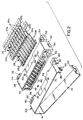
- the electrical connector system of the invention is incorporated in a mobile telephone system, generally designated 10, which includes a portable telephone handset, generally designated 12.
- the handset is insertable into and removable from a cradle or socket 14 defined in a housing 16 of a base unit, generally designated 18, of the mobile telephone system.
- the handset is inserted into and removed from the cradle generally in the direction of arrow "A". It can be understood that this direction is not precisely linear and can vary from use to use and depending on the actions of the user.
- female connector 22 includes terminals 26 and 28 coupled to a printed circuit board 30 within casing 22 of the handset; and male connector 24 includes terminals 32 and 34 coupled to a printed circuit board 36 within housing 16 of base unit 18.
- male and female connectors 24 and 20, respectively are elongated and mount transverse pairs of terminals 26 and 28 in female connector 20 and terminals 32 and 34 in male connector 24.
- the terminals may be signal and/or data terminals.
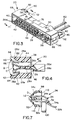
- female connector 20 includes a dielectric housing 38 unitarily molded of plastic material or the like. It can be seen that the housing is elongated and defines a longitudinal opening or slot 40 in a mating end 42 of the housing for receiving the mating end of male connector 24, as will be seen hereinafter.
- the housing defines a plurality of cavities 44 and 46 for mounting terminals 26 and 28, respectively.
- Housing 38 further includes a recessed area 48 and a pair of bosses 50 on the top thereof.
- a pair of mounting blocks 52 project rearwardly from the housing at opposite ends thereof, and mounting holes 54 are provided in the mounting blocks.
- the housing has a pair of sockets 56 (Fig. 2) at one end thereof for receiving a pair of coaxial connectors 58 (Fig. 3) which are terminated to a pair of coaxial cables 60.
- Terminals 26 and 28 have solder tails 26a and 28a at rear ends of spring arm portions 26b and 28b, respectively, for soldering to solder traces on printed circuit board 30 (Fig. 1).
- the spring arm portions extend forwardly in cavities 44 and 46.
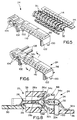
- Spring contact portions 26d and 28d are formed on the other or outer ends of terminals 26 and 28, respectively, and project outwardly of or are exposed at the mating end of female connector 20.
- the spring contact portions can be seen to be formed by generally U-shaped ends of the terminals bent outwardly and back along spring arm portions 26b and 28b of the terminals.
- Terminals 26 and 28 are stamped and formed from sheet metal material and are shown in Figure 2 still connected to carrier strips 67a and 67b, respectively, which are used during the manufacture of the terminals.
- the carrier strips are used for "gang" mounting or assembly of the terminals into cavities 44 and 46 of female connector housing 38.
- spring contact portions 26d and 28d of the terminals are configured so as to define a generally V-configured contacting area as indicated by double-headed arrow "C".
- female connector 20 is a shielded connector and includes a shield, generally designated 68.
- the shield is elongated for snugly embracing housing 38 and has an upper wall 70, a lower wall 72, and an end wall 74 integrally joining the upper and lower walls.
- the upper wall is provided with a depressed area 76 for seating in recessed area 48 of housing 38, along with a pair of holes 78 for receiving bosses 50 of the housing.
- the upper wall also includes a pair of rearwardly projecting flanges 80 having mounting holes 82 for alignment with mounting holes 54 in mounting blocks 52 of the housing, whereby appropriate fastening means 84 (Fig. 1) can be inserted through the aligned mounting holes for securement to a mounting boss 86 (Fig.
- top wall 70 of shield 60 has a depending end flange 88 with latch hooks 90 projecting therefrom.
- the latch hooks are snap fit into a slot 92 in the upper edge of a protruding boss 94 at one end of housing 38, with flange 88 overlying flange portions 96 projecting upwardly from bottom wall 72 of the shield, as best seen in Figure 3, when the shield embraces the housing.
- male connector 12 includes a dielectric housing 98 unitarily molded of plastic material or the like.
- the housing includes depending mounting pegs 100 for insertion into appropriate mounting holes in printed circuit board 36 (Fig. 1).
- Male connector housing 98 includes a pair of flanges 102 for insertion into the ends of longitudinal opening 40 in female connector housing 38.
- the male connector housing further includes a pair of sockets 104 at one end thereof for receiving a pair of coaxial connectors 106 (Fig. 6) which are terminated to a pair of coaxial cables 108, the connectors being mateable with coaxial connectors 58 (Fig. 3) mounted within female connector 24.
- male connector housing 98 has pairs of cavities 110 within which terminals 32 and 34 are mounted in pairs longitudinally of the connector.
- the housing has a generally V-shaped mating end 112 as best seen in Figure 7.
- terminals 32 and 34 of male connector 24 are stamped and formed from sheet metal material and are shown in Figure 5 still connected to carrier strips 114 which are used during the manufacture of the terminals.
- the carrier strips also are used for "gang" mounting or assembly of the terminals within cavities 110 of male connector housing 98.
- the terminals have spring arm portions 32a and 34a extending into cavities 110. It can be seen in Figure 5 that the spring arm portions are enlarged for press-fitting into the cavities.
- the terminals also include solder tail portions 32b and 34b for soldering to circuit traces on printed circuit board 36 (Fig. 1).
- terminals 32 and 34 include spring arm portions 32c and 34c, respectively, which are formed by U-shaped ends of the terminals bent outwardly and back along spring arm portions 32a and 34a.
- spring contact portions 32c and 34c combine to define a contacting area of a generally V-shaped configuration, as indicated by double-headed arrow "D".
- the outer surfaces of the spring contact portions in the unmated condition shown in Figure 7, are flush with mating end 112 of male connector housing 98.
- the included angle of the spring contact portions as represented by double-headed arrow "D" is the same as the angle defined by V-shaped mating end 112.
- Figure 8 shows male and female connectors 24 and 20, respectively, in an initial state of mating wherein spring contact portions 26d and 28d of the terminals of female connector 20 have made initial engagement with spring contact portions 34c and 32c of the terminals of male connector 24, yet the connectors are not as yet engaged or fully mated.
- the connectors are moved together from the initial stage shown in Figure 8, wherein the respective spring contact portions of the connectors already have engaged, to the fully mated condition shown in Figure 9, it can be seen that two things have taken place. First, the respective spring contact portions of the connectors have effected a considerable wiping action during mating.
Landscapes
- Coupling Device And Connection With Printed Circuit (AREA)
- Details Of Connecting Devices For Male And Female Coupling (AREA)
Claims (7)
- Elektrisches Verbindersystem, welches umfasst:erste (20) und zweite (24) elektrische Verbinder, welche in einer gegebenen allgemeinen Richtung (A) zusammenfügbar sind, wobei jeder Verbinder ein Gehäuse (38, 98) mit einem Paarungsende (42, 112) und wenigstens einem Paar von Kontakten (26/28, 32/34) aufweist, welche am jeweiligen Gehäuse befestigt sind, wobei das Paar von Kontakten jedes Verbinders Federkontaktabschnitte (26d/28d, 32c/34c) aufweist, welche mit den Federkontaktabschnitten des Paares von Kontakten des anderen Verbinders in Kontakt treten, wobei die Federkontaktabschnitte (26d/28d) der Kontakte des ersten Verbinders (20) derart ausgebildet sind, dass diese unter einem Winkel zur Zusammenfügerichtung zum Paarungsende (42) des ersten Verbinders hin in einer im Wesentlichen V-förmigen Ausbildung auseinanderlaufen, und die Federkontaktabschnitte (32c, 34c) der Kontakte des zweiten Verbinders (24) derart ausgebildet sind, dass diese unter einem Winkel zur Zusammenfügerichtung zum Paarungsende (112) des zweiten Verbinders hin in einer im Wesentlichen umgekehrten V-Ausbildung zusammenlaufen, wodurch die Federkontaktabschnitte der jeweiligen Verbinder während des Zusammenfügens der Verbinder einen Schleifkontakt bilden und beim Zusammenfügen der Verbinder Energie speichern können, das Trennen der Verbinder helfen kann,
dadurch gekennzeichnet, dassdie Federkontaktabschnitte (26d, 28d) des ersten Verbinders (20) unter einem Winkel zur Zusammenfügerichtung auseinanderlaufen, welcher kleiner ist als der Winkel, unter dem die Federkontaktabschnitte (32c, 34c) des zweiten Verbinders (34) relativ zur Zusammenfügerichtung zusammenlaufen. - Elektrisches Verbindersystem nach Anspruch 1,
bei welchem die Kontakte (26/28, 32/34) Federarmabschnitte (26b, 28b, 32a/34a) mit im Wesentlichen U-förmigen Enden umfassen, welche die Federkontaktabschnitte definieren. - Elektrisches Verbindersystem nach Anspruch 2,
bei welchem die U-förmigen Enden der Kontakte von den jeweiligen Federarmabschnitten der Kontakte nach außen gebogen sind. - Elektrisches Verbindersystem nach Anspruch 3,
bei welchem die Federarmabschnitte (26b, 28b) der Kontakte (26, 28) des ersten Verbinders (20) elastischer als die Federarmabschnitte (32a, 34a) der Kontakte (32, 34) des zweiten Verbinders (24) sind. - Elektrisches Verbindersystem nach Anspruch 4,
bei welchem das Gehäuse (38) des ersten Verbinders (20) eine Wand (62) zum Angreifen der U-förmigen Enden der Kontakte aufweist, um beim Zusammenfügen der Verbinder die U-förmigen Enden zusammenzupressen und außerdem darin Energie zu speichern. - Elektrisches Verbindersystem nach Anspruch 4,
bei welchem die Federkontaktabschnitte (26d, 28d) des ersten Verbinders (20) unter einem Winkel zu der Zusammenfügeeinrichtung auseinanderlaufen, welcher kleiner als der Winkel ist, unter dem die Federkontaktabschnitte (32c, 34c) des zweiten Verbinders (20) relativ zur Zusammenfügerichtung zusammenlaufen, wobei die Federkontaktabschnitte der jeweiligen Verbinder während des Zusammenfügens der Verbinder einen Schleifkontakt bilden und beim Zusammenfügen der Verbinder Energie speichern können, die beim Trennen der Verbinder helfen kann. - Elektrisches Verbindersystem, welches umfasst:erste (20) und zweite (24) elektrische Verbinder, welche in einer gegebenen allgemeinen Richtung (A) zusammenfügbar sind, wobei jeder Verbinder ein Gehäuse (38, 98) mit einem Paarungsende (42, 112) und wenigstens ein Paar von Kontakten (26/28, 32/34) aufweist, welche am Gehäuse befestigt sind, wobei das Paar von Kontakten jedes Verbinders Kontaktabschnitte (26d/28d, 32c/34c) aufweist, welche mit den Kontaktabschnitten des Paares von Kontakten des anderen Verbinders in Kontakt treten, wobei die Kontaktabschnitte der Kontakte eines Verbinders in einem Winkel zur Zusammenfügerichtung liegen, um eine im Wesentlichen V-förmige Ausbildung zu definieren, und wobei die Kontaktabschnitte der Kontakte eines der Verbinder elastisch sind, wodurch zwischen den jeweiligen Kontakten während des Zusammenfügens der Verbinder ein Schleifkontakt wirkt und die elastischen Kontaktabschnitte beim Zusammenfügen der Verbinder Energie speichern, die beim Trennen der Verbinder hilft, wobei die Kontaktabschnitte (26d, 28d) der Kontakte des ersten Verbinders (20) unter einem Winkel zur Zusammenfügerichtung auseinanderlaufen, um eine im Wesentlichen V-förmige Eingriffausbildung zu definieren,
dadurch gekennzeichnet, dassdie Kontaktabschnitte der Kontakte (26, 28) des ersten Verbinders (20) elastischer als die Kontaktabschnitte der Kontakte (32, 34) des zweiten Verbinders (24) sind.
Applications Claiming Priority (2)
| Application Number | Priority Date | Filing Date | Title |
|---|---|---|---|
| IE272292 | 1992-10-09 | ||
| IE272292A IE922722A1 (en) | 1992-10-09 | 1992-10-09 | Electrical connector system |
Publications (3)
| Publication Number | Publication Date |
|---|---|
| EP0591723A2 EP0591723A2 (de) | 1994-04-13 |
| EP0591723A3 EP0591723A3 (en) | 1996-07-31 |
| EP0591723B1 true EP0591723B1 (de) | 2000-12-13 |
Family
ID=11039771
Family Applications (1)
| Application Number | Title | Priority Date | Filing Date |
|---|---|---|---|
| EP93114805A Expired - Lifetime EP0591723B1 (de) | 1992-10-09 | 1993-09-15 | Elektrische Verbindervorrichtung |
Country Status (7)
| Country | Link |
|---|---|
| US (1) | US5387134A (de) |
| EP (1) | EP0591723B1 (de) |
| JP (1) | JP2550017Y2 (de) |
| KR (1) | KR0128487B1 (de) |
| DE (1) | DE69329747T2 (de) |
| FI (1) | FI109563B (de) |
| IE (1) | IE922722A1 (de) |
Cited By (1)
| Publication number | Priority date | Publication date | Assignee | Title |
|---|---|---|---|---|
| EP3796475B1 (de) * | 2019-09-18 | 2023-06-07 | Globe (Jiangsu) Co., Ltd. | Ladekupplung |
Families Citing this family (26)
| Publication number | Priority date | Publication date | Assignee | Title |
|---|---|---|---|---|
| GB2293283B (en) * | 1994-09-09 | 1999-02-24 | Nokia Mobile Phones Ltd | Combined connector contact |
| DE69609733T2 (de) * | 1995-03-16 | 2001-04-12 | The Whitaker Corp., Wilmington | Verbindungssystem für tragbares telefon |
| JPH0963716A (ja) * | 1995-08-25 | 1997-03-07 | Hirose Electric Co Ltd | 携帯電話機用複合コネクタ |
| DE19611423C1 (de) * | 1996-03-22 | 1997-05-22 | Siemens Ag | Elektrischer Verbinder |
| US5993231A (en) * | 1996-03-22 | 1999-11-30 | Siemens Aktiengesellschaft | Electric connector |
| FR2748150B1 (fr) * | 1996-04-26 | 1998-07-17 | Matra Communication | Plot de charge pour appareil portable a batterie rechargeable |
| FR2781090B1 (fr) * | 1998-07-09 | 2000-08-18 | Alsthom Cge Alcatel | Ensemble de connexion a pression |
| FR2781091B1 (fr) | 1998-07-09 | 2000-08-11 | Alsthom Cge Alcatel | Ensemble de connexion a insertion |
| FR2781094B1 (fr) | 1998-07-09 | 2000-08-18 | Alsthom Cge Alcatel | Ensemble de connexon mixte |
| JP3763703B2 (ja) * | 1999-06-02 | 2006-04-05 | 株式会社東芝 | 無線通信機および電池パックおよびコネクタ |
| US6354870B1 (en) * | 1999-08-12 | 2002-03-12 | Matsushita Mobil Communication Development Corp. | Apparatus and method for mounting small electrical connector |
| WO2001035498A1 (en) * | 1999-11-10 | 2001-05-17 | Framatome Connectors International | Receptacle and plug connectors |
| FR2800925B1 (fr) * | 1999-11-10 | 2001-12-07 | Framatome Connectors Int | Connecteur d'entree/sortie du type embase |
| JP2001293928A (ja) * | 2000-04-13 | 2001-10-23 | Jst Mfg Co Ltd | リセプタクル型コネクタ |
| US6293829B1 (en) * | 2000-08-25 | 2001-09-25 | Molex Incorporated | Electrical connector with wire management system |
| US6398577B1 (en) | 2000-10-04 | 2002-06-04 | Molex Incorporated | Latching/unlatching system for electrical connectors |
| US20030148740A1 (en) * | 2000-12-28 | 2003-08-07 | William Yau | Handset holder |
| US6558189B2 (en) * | 2001-03-14 | 2003-05-06 | Palm, Inc. | Connector system for use with handheld computers and accessory devices |
| US20020153863A1 (en) * | 2001-04-24 | 2002-10-24 | Arndt Steven W. | Charge contacts for rechargeable device |
| US6491527B1 (en) | 2001-05-17 | 2002-12-10 | Ericsson Inc. | Dual compression connector |
| JP3761428B2 (ja) * | 2001-07-04 | 2006-03-29 | 日本航空電子工業株式会社 | コネクタ |
| US7785152B2 (en) * | 2008-04-22 | 2010-08-31 | Hon Hai Precision Ind. Co., Ltd | High density connector having two-leveled contact interface |
| JP6254421B2 (ja) * | 2013-11-01 | 2017-12-27 | センサータ テクノロジーズ マサチューセッツ インコーポレーテッド | コネクター |
| JP6991782B2 (ja) | 2017-08-23 | 2022-01-13 | センサータ テクノロジーズ インコーポレーテッド | ソケット |
| WO2020039666A1 (ja) * | 2018-08-24 | 2020-02-27 | 株式会社村田製作所 | 電気コネクタセットおよび該電気コネクタセットの実装された回路基板 |
| CN118198756A (zh) * | 2019-08-01 | 2024-06-14 | 株式会社村田制作所 | 阴型多极连接器以及具备该阴型多极连接器的多极连接器组 |
Family Cites Families (10)
| Publication number | Priority date | Publication date | Assignee | Title |
|---|---|---|---|---|
| US2899669A (en) * | 1959-08-11 | Electrical connector | ||
| NL302480A (de) * | 1957-04-22 | |||
| JPS5124112B1 (de) * | 1971-06-24 | 1976-07-21 | ||
| US3950070A (en) * | 1974-06-25 | 1976-04-13 | Amp Incorporated | Flat flexible cable terminal and electrical interconnection system |
| US4026625A (en) * | 1975-11-10 | 1977-05-31 | Minnesota Mining And Manufacturing Company | Universal connector |
| JPS62177875A (ja) * | 1986-01-31 | 1987-08-04 | ケル株式会社 | フラツトケ−ブルコネクタ |
| US4715820A (en) * | 1986-09-29 | 1987-12-29 | Amp Incorporated | Connection system for printed circuit boards |
| US4734045A (en) * | 1987-03-27 | 1988-03-29 | Masterite Industries, Inc. | High density connector |
| US5052943A (en) * | 1989-03-23 | 1991-10-01 | Norand Corporation | Recharging and data retrieval apparatus |
| JP2551493Y2 (ja) * | 1992-07-14 | 1997-10-22 | ホシデン株式会社 | 脱着コネクタ |
-
1992
- 1992-10-09 IE IE272292A patent/IE922722A1/en not_active IP Right Cessation
-
1993
- 1993-07-09 US US08/090,394 patent/US5387134A/en not_active Expired - Fee Related
- 1993-09-08 JP JP1993053637U patent/JP2550017Y2/ja not_active Expired - Fee Related
- 1993-09-15 EP EP93114805A patent/EP0591723B1/de not_active Expired - Lifetime
- 1993-09-15 DE DE69329747T patent/DE69329747T2/de not_active Expired - Fee Related
- 1993-10-08 KR KR1019930020789A patent/KR0128487B1/ko not_active IP Right Cessation
- 1993-10-08 FI FI934449A patent/FI109563B/fi active
Cited By (1)
| Publication number | Priority date | Publication date | Assignee | Title |
|---|---|---|---|---|
| EP3796475B1 (de) * | 2019-09-18 | 2023-06-07 | Globe (Jiangsu) Co., Ltd. | Ladekupplung |
Also Published As
| Publication number | Publication date |
|---|---|
| JPH08527U (ja) | 1996-03-22 |
| KR0128487B1 (ko) | 1998-04-15 |
| EP0591723A2 (de) | 1994-04-13 |
| IE922722A1 (en) | 1994-04-20 |
| EP0591723A3 (en) | 1996-07-31 |
| US5387134A (en) | 1995-02-07 |
| DE69329747D1 (de) | 2001-01-18 |
| KR940010425A (ko) | 1994-05-26 |
| JP2550017Y2 (ja) | 1997-10-08 |
| DE69329747T2 (de) | 2001-06-07 |
| FI934449A0 (fi) | 1993-10-08 |
| FI109563B (fi) | 2002-08-30 |
| FI934449A (fi) | 1994-04-10 |
Similar Documents
| Publication | Publication Date | Title |
|---|---|---|
| EP0591723B1 (de) | Elektrische Verbindervorrichtung | |
| US5885088A (en) | Electrical connector assembly with polarization means | |
| EP0590517B1 (de) | Elektrischer Verbinder mit vorgespanntem federartigem Anschluss mit verbesserter schleifender Wirkung | |
| KR100231122B1 (ko) | 개선된 배치 수단을 갖는 전기 커넥터 | |
| US6183287B1 (en) | Electrical connector | |
| US5716230A (en) | Surface engageable electrical connector | |
| US6695628B2 (en) | Battery connector | |
| EP0717463A2 (de) | Flachprofil-, oberflächenmontierbare elektrische Verbinderanordnung | |
| EP0635909A1 (de) | Elektrischer Verbinder für gedruckte Schaltungen mit Befestigungselementen | |
| US6220898B1 (en) | Audio jack having means for reliably securing terminals thereof | |
| EP0630080A2 (de) | Leiterplatte mit darauf montierter modularen Telefonsteckerbuchse | |
| US5538435A (en) | Electrical input/output connector with switchable contacts | |
| US5338230A (en) | Electrical connector assembly | |
| US5354216A (en) | Mounting system for electrical connectors | |
| US6830469B1 (en) | Electrical connector assembly | |
| US6568963B2 (en) | Electrical connector assembly with improved contacts | |
| US6652302B1 (en) | Electrical connector with pivotable contact | |
| EP1276181B1 (de) | Elektrischer Verbinder zum Aufnahme eines Steckers | |
| JP3194215B2 (ja) | 電気コネクタアッセンブリとその嵌合保持力調整方法 | |
| US20010002346A1 (en) | Battery connector | |
| US6231390B1 (en) | Connector for use in portable phone | |
| US6146172A (en) | Electrical connector | |
| US20030104714A1 (en) | Electrical connector with highly compliant terminals | |
| IES59920B2 (en) | Electrical connector system | |
| CN214542623U (zh) | 电源连接器与连接组件 |
Legal Events
| Date | Code | Title | Description |
|---|---|---|---|
| PUAI | Public reference made under article 153(3) epc to a published international application that has entered the european phase |
Free format text: ORIGINAL CODE: 0009012 |
|
| AK | Designated contracting states |
Kind code of ref document: A2 Designated state(s): DE FR GB IT SE |
|
| PUAL | Search report despatched |
Free format text: ORIGINAL CODE: 0009013 |
|
| AK | Designated contracting states |
Kind code of ref document: A3 Designated state(s): DE FR GB IT SE |
|
| 17P | Request for examination filed |
Effective date: 19961213 |
|
| 17Q | First examination report despatched |
Effective date: 19981001 |
|
| GRAG | Despatch of communication of intention to grant |
Free format text: ORIGINAL CODE: EPIDOS AGRA |
|
| 17Q | First examination report despatched |
Effective date: 19981001 |
|
| GRAG | Despatch of communication of intention to grant |
Free format text: ORIGINAL CODE: EPIDOS AGRA |
|
| GRAH | Despatch of communication of intention to grant a patent |
Free format text: ORIGINAL CODE: EPIDOS IGRA |
|
| RIC1 | Information provided on ipc code assigned before grant |
Free format text: 7H 01R 24/00 A, 7H 01R 13/633 B, 7H 01R 13/635 B, 7H 01R 12/20 B, 7H 01R 13/24 B |
|
| GRAH | Despatch of communication of intention to grant a patent |
Free format text: ORIGINAL CODE: EPIDOS IGRA |
|
| ITF | It: translation for a ep patent filed | ||
| GRAA | (expected) grant |
Free format text: ORIGINAL CODE: 0009210 |
|
| AK | Designated contracting states |
Kind code of ref document: B1 Designated state(s): DE FR GB IT SE |
|
| REF | Corresponds to: |
Ref document number: 69329747 Country of ref document: DE Date of ref document: 20010118 |
|
| ET | Fr: translation filed | ||
| PLBE | No opposition filed within time limit |
Free format text: ORIGINAL CODE: 0009261 |
|
| STAA | Information on the status of an ep patent application or granted ep patent |
Free format text: STATUS: NO OPPOSITION FILED WITHIN TIME LIMIT |
|
| 26N | No opposition filed | ||
| REG | Reference to a national code |
Ref country code: GB Ref legal event code: IF02 |
|
| PGFP | Annual fee paid to national office [announced via postgrant information from national office to epo] |
Ref country code: GB Payment date: 20020808 Year of fee payment: 10 |
|
| PGFP | Annual fee paid to national office [announced via postgrant information from national office to epo] |
Ref country code: FR Payment date: 20020903 Year of fee payment: 10 |
|
| PGFP | Annual fee paid to national office [announced via postgrant information from national office to epo] |
Ref country code: SE Payment date: 20020904 Year of fee payment: 10 |
|
| PGFP | Annual fee paid to national office [announced via postgrant information from national office to epo] |
Ref country code: DE Payment date: 20020930 Year of fee payment: 10 |
|
| PG25 | Lapsed in a contracting state [announced via postgrant information from national office to epo] |
Ref country code: GB Free format text: LAPSE BECAUSE OF NON-PAYMENT OF DUE FEES Effective date: 20030915 |
|
| PG25 | Lapsed in a contracting state [announced via postgrant information from national office to epo] |
Ref country code: SE Free format text: LAPSE BECAUSE OF NON-PAYMENT OF DUE FEES Effective date: 20030916 |
|
| PG25 | Lapsed in a contracting state [announced via postgrant information from national office to epo] |
Ref country code: DE Free format text: LAPSE BECAUSE OF NON-PAYMENT OF DUE FEES Effective date: 20040401 |
|
| EUG | Se: european patent has lapsed | ||
| GBPC | Gb: european patent ceased through non-payment of renewal fee |
Effective date: 20030915 |
|
| PG25 | Lapsed in a contracting state [announced via postgrant information from national office to epo] |
Ref country code: FR Free format text: LAPSE BECAUSE OF NON-PAYMENT OF DUE FEES Effective date: 20040528 |
|
| REG | Reference to a national code |
Ref country code: FR Ref legal event code: ST |
|
| PG25 | Lapsed in a contracting state [announced via postgrant information from national office to epo] |
Ref country code: IT Free format text: LAPSE BECAUSE OF NON-PAYMENT OF DUE FEES Effective date: 20050915 |