EP0590122B1 - Verfahren zur übertragung serieller datenstrukturen für informationsträgeridentifikationssysteme, danach arbeitendes übertragungssystem und informationsträger - Google Patents
Verfahren zur übertragung serieller datenstrukturen für informationsträgeridentifikationssysteme, danach arbeitendes übertragungssystem und informationsträger Download PDFInfo
- Publication number
- EP0590122B1 EP0590122B1 EP93907839A EP93907839A EP0590122B1 EP 0590122 B1 EP0590122 B1 EP 0590122B1 EP 93907839 A EP93907839 A EP 93907839A EP 93907839 A EP93907839 A EP 93907839A EP 0590122 B1 EP0590122 B1 EP 0590122B1
- Authority
- EP
- European Patent Office
- Prior art keywords
- information carrier
- data
- coil
- data structures
- carrier
- Prior art date
- Legal status (The legal status is an assumption and is not a legal conclusion. Google has not performed a legal analysis and makes no representation as to the accuracy of the status listed.)
- Expired - Lifetime
Links
Images


Classifications
-
- G—PHYSICS
- G06—COMPUTING OR CALCULATING; COUNTING
- G06K—GRAPHICAL DATA READING; PRESENTATION OF DATA; RECORD CARRIERS; HANDLING RECORD CARRIERS
- G06K19/00—Record carriers for use with machines and with at least a part designed to carry digital markings
- G06K19/06—Record carriers for use with machines and with at least a part designed to carry digital markings characterised by the kind of the digital marking, e.g. shape, nature, code
- G06K19/067—Record carriers with conductive marks, printed circuits or semiconductor circuit elements, e.g. credit or identity cards also with resonating or responding marks without active components
- G06K19/07—Record carriers with conductive marks, printed circuits or semiconductor circuit elements, e.g. credit or identity cards also with resonating or responding marks without active components with integrated circuit chips
- G06K19/0723—Record carriers with conductive marks, printed circuits or semiconductor circuit elements, e.g. credit or identity cards also with resonating or responding marks without active components with integrated circuit chips the record carrier comprising an arrangement for non-contact communication, e.g. wireless communication circuits on transponder cards, non-contact smart cards or RFIDs
-
- G—PHYSICS
- G06—COMPUTING OR CALCULATING; COUNTING
- G06K—GRAPHICAL DATA READING; PRESENTATION OF DATA; RECORD CARRIERS; HANDLING RECORD CARRIERS
- G06K7/00—Methods or arrangements for sensing record carriers, e.g. for reading patterns
- G06K7/0008—General problems related to the reading of electronic memory record carriers, independent of its reading method, e.g. power transfer
Definitions
- the invention relates to a method for the transmission of serial data structures for information carrier identification systems and a transmission system operating thereupon based on contactless, electromagnetic transmission and to an information carrier which can be used therefor.
- identification systems have become known in particular through separate chip cards and tool data carriers.
- the known identification systems that use integrated chips on the information carrier side have the disadvantage that they require a power-consuming intermediate storage device on the information carrier, which realizes a data comparison, requires relatively high energies for data transmission, there is a relatively high data uncertainty and the time for data transmission and the data comparison for some use cases is relatively long.
- the invention is therefore based on the object of specifying an information carrier identification system and a method for transmitting serial data structures that circumvents the disadvantages of the prior art.
- an identification system consists of an interface module and an information carrier.
- the interface module is used to implement data communication between any computer and the information carrier.
- a microcontroller, microprocessor or freely programmable logic which produces the data coupling, for example, to a computer, and at the same time the necessary control and command signals as well as serial data inputs and outputs specially tailored to the information carrier provides (SD1 and SD2 in Fig. 1).
- the data output of the microcontroller or a module comparable to it carries a serial data structure to a digital comparator which compares the transmitted data bit by bit and clocked with a serial data structure received via an AM demodulator.
- the result of the comparison is sent to the microcontroller or the like via a line I10. given and evaluated in this.
- Clock pulses for a clocked comparison are supplied via a control line S10 (corresponding to FIG. 4).
- the data comparison can be edge-controlled by setting a flip-flop or static.
- the function of the digital comparator can be implemented on the interface side and / or on the information carrier side (in the following, however, only the interface-side attachment will be carried out further).
- the data levels high and low are converted into two frequency positions or phase positions.
- a carrier T10 modulated in this way drives a resonant circuit via a power stage.
- the carrier frequency T10 Via the magnetic coupling of a coil L1 of the resonant circuit, the carrier frequency T10 induces an alternating voltage following the carrier frequency into the information carrier, preferably via L2.
- An input circuit L2 on the information carrier can be tuned to resonance with an integrated capacitance C2. It is of course within the scope of the invention to work on the primary and secondary side without resonance transmission instead of a complete resonant circuit, ie that only parasitic capacitances act for C2.
- a rectification generates an internal operating voltage from the HF voltage.
- the carrier frequency is tapped via a resonant circuit L2 of the information carrier and digitized in a comparator.
- the clock and data signals are obtained in a demodulator of the information carrier according to conventional, integration-friendly methods, depending on the selected modulation type of the interface.
- a serial data signal D1 is not only fed to a control logic, but in particular is switched through to an amplitude modulator via an electronic switch.
- the amplitude modulator dampens a coil L3 of the information carrier in time with the subcarrier T2, which in turn is clocked out or on in time with a received data signal D4. Due to the inductive coupling to the coil L1, after a selective amplification on the frequency of an auxiliary carrier and a simple amplitude demodulation, the signal returned by the information carrier can be compared by means of the digital comparator.
- the data transmission between the interface and the information carrier begins with the generation of an operating voltage by the voltage induced by the carrier signal in L2.
- the rectified voltage across a smoothing capacitance C3 and optionally the operating voltage are evaluated by an evaluation circuit and used for further use.
- a predefinable voltage level of the voltage across C3 is used to control the transmission energy of the interface.
- the information is given to the control logic of the information carrier via a bus line S1, a status signal D2 is given to the interface via a digital multiplexer and AM modulator. After evaluation in the microcontroller or similar. control of the power driver stage via S20 in such a way that a voltage overload at L2 in the information carrier is avoided.
- the further program sequence can be predetermined by a program counter and control logic, which are connected via setting and control lines S2 and S3.
- serial data information D2 can preferably be given once or repetitively, or in particular in the case of code carriers, serial data information D2 (status signal) and then automatically controlled by the control logic and D4 can transmit permanently coded information to the AM modulator via the digital multiplexer will.
- the data information D2 is evaluated in the interface for a further program run. When the readiness to receive is established, the program counter for data carriers is reset to the start position and only started after a data word D1 via S2 has been applied.
- the received data which consist of control, address and data words, are decoded in the control logic.
- the program instructions are read from the control word and stored in a static memory.
- the generally known communications run with a non-volatile memory, for example a 2Kbit E 2 PROM, via lines D3, S4 and D4.
- the digital multiplexer switches through to an AM modulator in a controlled manner.
- the evaluation circuit resets the logic via S1, and the functional sequence can start again with the start phase if the carrier is again is switched on.
- the advantages of the invention are that by a time parallel Data transmission of data sent and received again Information storage-side, power-consuming buffers can be dispensed with, which results in a significant simplification in the circuit structure of the information carrier results in less energy for Data transmission is required, the time for data transmission is measured is shortened at the state of the art and at the same time high Data security is achieved.
- Another advantage of Overall system according to the invention is that one and the same Transmission system for both data carriers and bare ones Code carrier can be used.
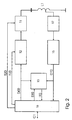
- FIG. 1 shows a coupling of a general data processing system via a connection C1 to an interface consisting of digital and analog modules with an electromagnetic coupling via L1 to L2 and L3 to an information carrier, which is preferably implemented by CMOS-ASIC.
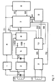
- FIG. 2 shows the actual interface part, which is weakly outlined in FIG. 1, in more detail. This essentially consists of a microprocessor or a microcontroller or a freely programmable logic 16, a digital comparator 13, a PSK modulator 12, a demodulator 15, a power driver 11 and a selective amplifier 17. In the same way in FIG.
- the start of the system sequence begins with a Interface-side sending of a high-frequency carrier signal with a Duty cycle 1: 1 via the inductance L1 acting as an antenna.
- a power driver 11 via a PSK modulator 12 in the interface controlled with a digital signal D00.
- the signal corresponds to D00 the logical state L of a serial data signal.
- a control line S20 sets the power driver to maximum transmit power or starts slowly, in a predeterminable time period (approx. 1 ms), the transmission power to control to a maximum.
- a clock T10 delivers one to the modulator 12 synchronous carrier frequency to the data signal.
- Via S10 a Digital comparator 13 deactivated, i.e. I10 delivers regardless of logical state D00 to D10 always a positive data comparison of the Digital comparator (see Fig. 2).
- the carrier signal When the carrier signal is sent, it builds up, if in the transmission range of L1 present, in an information carrier (data or code carrier) through transformer coupling using L2 and subsequent rectification 2 an operating voltage above a Smoothing capacitor C3 on. Is this tension sufficient? Value reached by means of a voltage stabilizer 5 or can produce several stabilized DC voltages VCC and one certain energy reserve for starting further circuits of the Holds information carrier ready, enters a power-on reset circuit 6 static start signal S1 to a control logic 7. Set until then Functions are released at the start.
- a Digital multiplexer 10 essential to the invention from the control logic 7 via S5 controlled so that it switches through a channel for D2.
- This signal is a serial password (e.g.
- a demodulator 15 provides the corresponding digitized serial password.
- the interface analyzes a known password, it starts any programmable sequence according to the Password content.
- the password contain a structure which indicates that a code carrier is in the reception area.
- the Sequence control in the interface would then not be the digital comparator 13 activate and read in further serial data structures.
- the carrier can then use the data length (e.g. also encrypted in the password) be switched off.
- the password can e.g. also digitally encodes the level of operating voltage in the information carrier contain. If there is sufficient voltage, the interface can reduce the transmission power via S20.
- serial data transmission from the interface to the information carrier begins with a start bit.
- the digital comparator 13 is activated and a bit-related data comparison is carried out.
- a prerequisite for a bit-related data comparison is that the total of the signal delays, switch-on and switch-off times in the transmission chain are less than one bit length (cf. FIG. 4).
- the data comparison can be edge-controlled using a flip-flop or static.
- the clock pulses are provided via the control line S10.
- the digital comparator 13 If the bit comparison turns out negative, the digital comparator 13 outputs an information signal to the microprocessor or microcontroller or to a freely programmable logic 16 via I1.
- the logic immediately switches off the carrier signal by setting S20 or switching off the clock T10 (carrier frequency). Since no more energy is now transferred to the information carrier, the operating voltage via C3 collapses very quickly and drops to a predetermined switch-off voltage of the power-on-reset circuit 6.
- the program sequences started in the information carrier are reset in a defined manner. The information carrier must now be restarted as described under 2.
- the start bit in the information carrier triggers the start to serial Receive data from. This means a synchronization of the control logic 7 and a program counter 8 and a switchover of a digital one Multiplexers 10 on channel D1. So the received signal becomes Modulator 3 of the information carrier passed and to the interface sent back.
- the serial sent from the interface after the start bit Data record contains a control word, a data address and, if applicable, a Data word. It makes sense to send the control word first, as with this the program sequence control in the control logic 7 of the Information carrier can be programmed.
- the program flow in the information carrier takes place according to the control word and the implemented programs.
- the programs are permanently "wired" in the control logic 7 and control the program counter 8, the digital multiplexer 10 and a memory 9 during the entire data transmission from the interface to the information carrier.
- the multiplexer 10 is switched synchronously to channel D4, controlled by the control logic 7 and the program counter 8, as a result of which the serial data flow from the memory 9 to the modulator 3 is switched.
- the switchover of the multiplexer 10 from D1 to D4 can be determined by the program counter 8 and the control logic 7 or controlled depending on the content of the control word in the data record.
- position D4 can be skipped when programming the memory 9 and a special password for the working state programming of the memory can be switched through.
- the multiplexer 10 switches back to channel D1.
- the password is sent again continuously, which can also contain changeable status signals.
- the following can be sent in the password: an information carrier identifier, a customer-specific code, a digitized operating voltage in the information carrier, the working state of the memory (eg with E 2 PROM in write mode: Write in progress).
- a special method requires the modulated Data signals in the energy carrier from returned data of the Separate information carrier.
- this is another Carrier (subcarrier) used by selective means in the interface from the energy source at a certain minimum distance between the two Frequencies and different types of modulation are separated can.
- the information returned can be marked with a AM demodulator that recovers the subcarrier in the interface and selectively amplified as well as a phase demodulator that the phase position of the auxiliary carrier in accordance with the data information, are received much more sensitively.
Landscapes
- Engineering & Computer Science (AREA)
- Physics & Mathematics (AREA)
- General Physics & Mathematics (AREA)
- Theoretical Computer Science (AREA)
- Computer Networks & Wireless Communication (AREA)
- Computer Hardware Design (AREA)
- Microelectronics & Electronic Packaging (AREA)
- Artificial Intelligence (AREA)
- Computer Vision & Pattern Recognition (AREA)
- Near-Field Transmission Systems (AREA)
- Radar Systems Or Details Thereof (AREA)
Description
Der Erfindung liegt somit die Aufgabe zugrunde, ein Informationsträgeridentifikationssystem und ein Verfahren zur Übertragung serieller Datenstrukturen anzugeben, daß die Nachteile des Standes der Technik umgeht.
Ein Identifikationssystem besteht gemäß der Erfindung aus einem Interfacebaustein und einem Informationsträger. Mit dem Interfacebaustein wird die Datenkommunikation zwischen beliebigen Computern und dem Informationsträger realisiert. Zur praktischen Lösung dieser Aufgabe verwendet man sinnvollerweise einen Mikrocontroler, Mikroprozessor bzw. eine frei programmierbare Logik, der bzw. die die Datenkopplung bspw. zu einem Computer herstellt und gleichzeitig notwendige Steuer- und Befehlssignale sowie speziell auf den Informationsträger zugeschnittene serielle Datenein- und -ausgänge bereitstellt (SD1 und SD2 in Fig. 1). Der Datenausgang des Mikrocontrolers bzw. ihm vergleichbarer Baugruppe führt eine serielle Datenstruktur an einen Digitalkomparator, der die ausgesendeten Daten bitweise und getaktet mit einer über einen AM-Demodulator empfangenen seriellen Datenstruktur vergleicht. Das Ergebnis des Vergleiches wird über eine Leitung I10 an den Mikrocontroler o.ä. gegeben und in diesem ausgewertet. Taktimpulse für einen getakteten Vergleich werden über eine Steuerleitung S10 (entsprechend Fig. 4) geliefert. Der Datenvergleich kann flankengesteuert durch Setzen eines Flip-Flop's oder statisch erfolgen. Die Taktflanke für S10 darf frühestens nach einer Zeit tv+ta (tv = Signalverzögerungszeit, ta= Signalanstiegszeit) gesetzt werden. Ebenso kann die Funktion des Digitalkomparators interfaceseitig und/oder auf der Informationsträgerseite realisiert werden (im folgenden wird jedoch nur die interfaceseitige Anbringung weiter ausgeführt). In einem FSK/PSK-Modulator werden die Datenlevel High und Low in zwei Frequenzlagen bzw. Phasenlagen gewandelt. Ein auf diese Weise modulierter Träger T10 treibt über eine Leistungsstufe einen Schwingkreis. Über die magnetische Kopplung einer Spule L1 des Schwingkreises induziert die Trägerfrequenz T10 in den Informationsträger vorzugsweise über L2 eine der Trägerfrequenz folgende Wechselspannung. Ein Eingangskreis L2 am Informationsträger kann mit einer integrierten Kapazität C2 auf Resonanz abgestimmt sein. Es liegt selbstverständlich im Rahmen der Erfindung, statt eines kompletten Schwingkreises primär- und sekundärseitig ohne Resonanzübertragung zu arbeiten, d.h. daß bspw. für C2 nur parasitäre Kapazitäten wirken. Eine Gleichrichtung erzeugt aus der HF-Spannung eine interne Betriebsspannung. Über einen Schwingkreis L2 des Informationsträgers wird die Trägerfrequenz abgegriffen und in einem Komparator digitalisiert. Die Gewinnung der Takt- und Datensignale erfolgt nach konventionellen integrationsfreundlichen Methoden in Abhängigkeit von der gewählten Modulationsart des Interface in einem Demodulator des Informationsträgers. Gemäß der Erfindung wird ein serielles Datensignal D1 nicht nur einer Steuerlogik zugeführt, sondern insbesondere über einen elektronischen Schalter an einen Amplitudenmodulator durchgeschaltet. Der Amplitudenmodulator dämpft eine Spule L3 des Informationsträgers im Takt eines Hilfsträgers T2, der wiederum im Rhythmus eines empfangenen Datensignals D4 aus- bzw. aufgetaktet wird. Durch die induktive Kopplung zur Spule L1 kann nach einer selektiven Verstärkung auf der Frequenz eines Hilfsträgers und einer einfachen Amplitudendemodulation das vom Informationsträger rückgesandte Signal mittels des Digitalkomparators verglichen werden.
- Fig. 1
- blockschaltartig die wesentlichen Bestandteile erfindungsgemäßen Übertragungssystems,
- Fig. 2
- eine detailliertere Darstellung der wesentlichen interfaceseitigen Baugruppen und ihr Zusammenwirken,
- Fig. 3
- eine Darstellung der wesentlichen informationsträgerseitigen Baugruppen und ihr Zusammenwirken und
- Fig. 4
- ein Beispiel für interface- und informationsträgerseitige Datenstrukturen in ihren Beziehungen zueinander.
Im folgenden soll der gesamte, mit der Erfindung realisierbare Systemablauf beschrieben werden.
Claims (9)
- Verfahren zur Übertragung serieller Datenstrukturen für Informationsträgeridentifikationssysteme auf induktiver Basis, in dem in einer Sendeeinheit ein Sendeschwingkreis mit frequenz- bzw. phasenmodulierten Datenstrukturen beaufschlagt wird die ausgesandten elektromagnetischen Schwingungen von einem Informationsträger empfangen werden, nach erfolgter Frequenz- bzw. Phasendemodulation die Datenstrukturen im Informationsträger decodiert, gelesen oder gespeichert werden dadurch gekennzeichnet, daß diese Datenstrukturen ihrerseits zugleich während des Empfangs amplitudenmoduliert zeitparallel der Sendeeinheit zurückgesandt werden, wo nach erfolgter Amplitudendemodulation unmittelbar ein bitweiser Kontrollvergleich mit der ausgesandten Datenstruktur vorgenommen wird und dieser Vorgang bei negativem Datenvergleich sofort oder am Ende eines Datenwortes oder Datensatzes abgebrochen wird und im weiteren so oft wiederholt wird, bis ausgesandte und wieder empfangene Datenstrukturen identisch sind.
- Verfahren nach Anspruch 1, dadurch gekennzeichnet, daß bei negativem Datenvergleich sofort oder am Ende eines Datenwortes durch Abschalten des Energieträgers und Abfall der Betriebsspannung auf dem Informationsträger die Datenübertragung abgebrochen wird und bei neuem Einschalten des Energieträgers auf dem Informationsträger ein Reset ausgelöst wird.
- Verfahren nach Anspruch 1, dadurch gekennzeichnet, daß bei negativem Datenvergleich der Informationsträger über seine Steuerlogik vermittels eines ihm übersandten Kontrollbits zurückgesetzt wird und dieser Vorgang so oft wiederholt wird, bis ausgesandte und wieder empfangene Datenstrukturen identisch sind.
- Verfahren nach Anspruch 1 und 2 oder 3, dadurch gekennzeichnet, daß, die von einer Quelle einer Mikrocontroler-Logik-Einheit o.ä. zugeleiteten Datenstrukturen einer Frequenz- bzw. Phasenmodulation unterworfen und leistungsverstärkt einem Sendeschwingkreis zugeführt werden, die dort ausgesandten elektromagnetischen Schwingungen von einem Schwingkreis eines integrierten Informationsträgers empfangen werden, in dem durch HF-Gleichrichtung in bekannter Weise dessen Betriebsspannung erzeugt wird, die Trägerfrequenz in einem Komparator abgegriffen und digitalisiert wird und eine Takt-, Synchronisations- und Frequenzbzw. Phasendemodulation in einer entsprechenden nachfolgenden Einheit durchgeführt wird und die danach gewonnen Signale einer Steuerlogik und zugleich über einen integrierten Schalter, der in Abhängigkeit von der bit- bzw. Byte-Breite der übertragenen Datenstrukturen in einem vorgebbaren Sende- und Empfangstakt geschaltet wird, diese Signale an einen Amplitudenmodulator durchgeschaltet werden, der eine Spule dämpft, die von der Spule ausgehende elektromagnetische Schwingung dem Sendeschwingkreis zugeführt und nach selektiver Verstärkung die empfangenen Signale einem Amplitudendemodulator zugeführt werden, wonach in einem Komparator ein unmittelbarer Datenvergleich zwischen gesendeten und empfangenen Datenstrukturen durchgeführt wird und im Falle der Nichtübereinstimmung der Informationsträger zurückgesetzt wird und ggf. unmittelbar folgend dieselbe Datenstruktur erneut bis zur festzustellenden Übereinstimmung ausgesendet wird, worauf sich anschließend weitere Datenstrukturen übertragen werden können.
- Verfahren nach einem der vorstehenden Ansprüche, dadurch gekennzeichnet, daß zur Dämpfung des elektromagnetischen Feldes ein Hilfsträger (T2) für das amplitudenmodulierte Rücksenden von seriellen Datenstrukturen benutzt wird, der eine Selektion der an der Sendespule (L1) liegenden modulierten Information der Informationsträgersendespule L3 vom modulierten Energieträger der Leistungsstufe (11) ermöglicht.
- Übertragungssystem zur Übertragung serieller Datenstrukturen für Informationsträgeridentifikationssysteme auf elektromagnetischer Basis, eine Interface-Baugruppe (11; 12; 15; 16; 17) zur Aufnahme, Verarbeitung und Weiterleitung von Daten einer Quelle, einen integrierten Informationsträger (1; 2; 3; 4; 5; 6; 7; 8; 9) mit Phasen- bzw. Frequenzdemodulator (4) und Schwingkreise zur Informationsübertragung enthaltend, wobei im Interface ein Frequenz- bzw. Phasenmodulator (12) vorgesehen ist, der eine Modulation von Quellendaten vornimmt, dadurch gekennzeichnet, daß diesem ein Leistungstreiber (11) nachgeordnet ist, der mit einem Schwingkreis in Verbindung steht, welcher seinerseits über einen selektiven Verstärker (17) mit einem Demodulator (15) verbunden ist und über einen Digitalkomparator (13) eine Verbindung zu einem Mikroprozessor oder einem Mikrocontroler oder einer freiprogrammierbaren Logik (16) hergestellt ist, über eine elektromagnetische Kopplung genannter Schwingkreis (L1) mit einem Schwingkreis (L2, L3) eines Informationsträgers gekoppelt ist, wobei dieser neben an sich bekannten Einzelelementen, wie Eingangsgleichrichter (2), Takt- und Synchronisationsmodulator einen Frequenz- bzw. Phasendemodulator (4) und einen Amplitudenmodulator (3) enthält, die miteinander in einem vorgebbaren Taktverhältnis über einen elektronischen Schalter (10) direkt bzw. wechselweise über eine Steuerlogik (7) in Verbindung gebracht sind, die ihrerseits darüber hinaus mit einem Programmzähler (8) und einem Speicher (9) in Verbindung steht, und daß der Ausgang des Frequenz- bzw. Phasendemodulators (4) zur gleichzeitigen Rückübertragung empfangener Daten mit dem Eingang des Amplitudenmodulators (3) verbindbar ist, und daß der Digitalkomparator (13) der Interface-Baugruppe für den bitweisen Datenvergleich gerade gesendeter Bits mit den vom Informationsträger zeitgleich zurückgesendeten Bits vorgesehen ist.
- Informationsträger für ein Identifikationssystem auf induktiver Basis, einen Empfangsschwingkreis, der eine Spule (L2) beinhaltet, einen Komparator (1) einen Phasen- bzw. Frequenzdemodulator (4), Mittel zur Spannungsgleichrichtung (2) und -stabilisierung (5), eine Steuerlogik (7) und einen Programmzähler (8) enthaltend, dadurch gekennzeichnet, daß ein Digitalmultiplexer (10) vorgesehen ist, der mit dem Demodulator (4), dessen Ausgang zur gleichzeitigen Rückübertragung empfangener Daten mit dem Eingang eines Amplitudendemodulators (3) verbindbar ist, der Steuerlogik (7) und einem nichtflüchtigen Speicher (9) in Verbindung gebracht ist und vom Amplitudenmodulator (3) aus eine Sendespule (L3) das Feld einer Sendespule (L1) eines Interface modulieren läßt.
- Informationsträger nach Anspruch 7, dadurch gekennzeichnet, daß die Sendespule (L3) des Informationsträgers so dimensioniert ist, daß die durch die Sendespule (L1) induzierte Spannung über der Sendespule (L3) so klein bleibt, daß sie von einem integrierten Schalter bedämpft werden kann und die dadurch hervorgerufene Dämpfung der durch die Spule (L1) induzierten Spannung über der Empfangsspule (L2) des Informationsträgers kleiner als 20% bleibt.
- Informationsträger nach Anspruch 8., dadurch gekennzeichnet, daß die Spulen (L2, L3) im wesentlichen koaxial in einer Ebene angeordnet sind und die Spulenachsen im wesentlichen achsparallel zur Spulenachse der Sendespule (L1) verlaufend festgelegt sind.
Applications Claiming Priority (3)
| Application Number | Priority Date | Filing Date | Title |
|---|---|---|---|
| DE4210669 | 1992-03-31 | ||
| DE4210669 | 1992-03-31 | ||
| PCT/EP1993/000748 WO1993020531A1 (de) | 1992-03-31 | 1993-03-26 | Verfahren zur übertragung serieller datenstrukturen für informationsträgeridentifikationssysteme, danach arbeitendes übertragungssystem und informationsträger |
Publications (2)
| Publication Number | Publication Date |
|---|---|
| EP0590122A1 EP0590122A1 (de) | 1994-04-06 |
| EP0590122B1 true EP0590122B1 (de) | 1998-06-10 |
Family
ID=6455610
Family Applications (1)
| Application Number | Title | Priority Date | Filing Date |
|---|---|---|---|
| EP93907839A Expired - Lifetime EP0590122B1 (de) | 1992-03-31 | 1993-03-26 | Verfahren zur übertragung serieller datenstrukturen für informationsträgeridentifikationssysteme, danach arbeitendes übertragungssystem und informationsträger |
Country Status (4)
| Country | Link |
|---|---|
| US (1) | US5519729A (de) |
| EP (1) | EP0590122B1 (de) |
| AT (1) | ATE167317T1 (de) |
| WO (1) | WO1993020531A1 (de) |
Families Citing this family (29)
| Publication number | Priority date | Publication date | Assignee | Title |
|---|---|---|---|---|
| US6472975B1 (en) * | 1994-06-20 | 2002-10-29 | Avid Marketing, Inc. | Electronic identification system with improved sensitivity |
| EP0738984B1 (de) * | 1995-04-18 | 1999-03-03 | EM Microelectronic-Marin SA | System zur Identifizierung von Gegenständen |
| DE29514235U1 (de) * | 1995-09-05 | 1996-06-05 | Siemens AG, 80333 München | Vorrichtung zur berührungslosen Übertragung von Daten an mobile Datenträger mit Annäherungsschutz |
| US5949826A (en) * | 1995-12-22 | 1999-09-07 | Matsushita Electric Industrial Co., Ltd. | Data transmission and reception system |
| US6167094A (en) * | 1996-10-15 | 2000-12-26 | Siemens Aktiengesellschaft | Data transmission circuit having a station and a response circuit |
| GB2321745B (en) * | 1997-01-30 | 2001-02-14 | Motorola Inc | Apparatus and method for recovering a clock signal for use in a portable data carrier |
| JP2000508955A (ja) * | 1997-02-13 | 2000-07-18 | ジカン・エフ・ウント・エー・ゲーエムベーハー | 患者データの体内測定のための移植可能測定装置 |
| US6747548B1 (en) * | 1997-06-18 | 2004-06-08 | Mitsubishi Denki Kabushiki Kaisha | Non-contact IC card system and non-contact IC card |
| EP0976204B1 (de) * | 1998-02-17 | 2005-11-30 | Koninklijke Philips Electronics N.V. | Sende/empfangsstation mit impedanzangepassten empfangsmitteln für transponderantwortsignale |
| GB9805896D0 (en) | 1998-03-20 | 1998-05-13 | Eglise David | Remote analysis system |
| KR100406565B1 (ko) | 1998-12-30 | 2004-03-24 | 주식회사 하이닉스반도체 | 데이타전송장치 |
| EP1141879B1 (de) * | 1999-10-22 | 2013-08-07 | Nxp B.V. | Datenträger mit lastabhängigem modulationsmittel und mit verbesserter stromversorgungseinrichtung im lastabhängigem modulationsprozess |
| US7456826B2 (en) * | 2002-02-28 | 2008-11-25 | Reinhard Jurisch | Touchscreen-sensitive and transponder reading stylus |
| JP2004138958A (ja) * | 2002-10-21 | 2004-05-13 | Semiconductor Energy Lab Co Ltd | 表示装置 |
| JP4519476B2 (ja) * | 2004-02-03 | 2010-08-04 | 株式会社東芝 | 無線通信装置 |
| US7327802B2 (en) * | 2004-03-19 | 2008-02-05 | Sirit Technologies Inc. | Method and apparatus for canceling the transmitted signal in a homodyne duplex transceiver |
| WO2007127948A2 (en) | 2006-04-27 | 2007-11-08 | Sirit Technologies Inc. | Adjusting parameters associated with leakage signals |
| US8248212B2 (en) | 2007-05-24 | 2012-08-21 | Sirit Inc. | Pipelining processes in a RF reader |
| EP2023661A1 (de) * | 2007-07-26 | 2009-02-11 | Oticon A/S | Kommunikationsvorrichtung, -system und -verfahren unter Verwendung induktiver Kommunikation |
| US8427316B2 (en) | 2008-03-20 | 2013-04-23 | 3M Innovative Properties Company | Detecting tampered with radio frequency identification tags |
| US8446256B2 (en) * | 2008-05-19 | 2013-05-21 | Sirit Technologies Inc. | Multiplexing radio frequency signals |
| US8169312B2 (en) * | 2009-01-09 | 2012-05-01 | Sirit Inc. | Determining speeds of radio frequency tags |
| DE102009019657A1 (de) * | 2009-04-30 | 2011-08-18 | Fraunhofer-Gesellschaft zur Förderung der angewandten Forschung e.V., 80686 | Vorrichtung und Verfahren zur Energieversorgung eines RFID-Bauteils |
| US20100289623A1 (en) * | 2009-05-13 | 2010-11-18 | Roesner Bruce B | Interrogating radio frequency identification (rfid) tags |
| US8416079B2 (en) * | 2009-06-02 | 2013-04-09 | 3M Innovative Properties Company | Switching radio frequency identification (RFID) tags |
| US20110205025A1 (en) * | 2010-02-23 | 2011-08-25 | Sirit Technologies Inc. | Converting between different radio frequencies |
| US10062025B2 (en) | 2012-03-09 | 2018-08-28 | Neology, Inc. | Switchable RFID tag |
| US9754137B2 (en) * | 2015-06-16 | 2017-09-05 | Motorola Mobility Llc | On-demand activation of radio frequency identification (RFID) tag |
| KR102731652B1 (ko) * | 2022-09-18 | 2024-11-19 | 쓰리에이로직스(주) | 듀얼 밴드 rfid 태그와 이를 포함하는 감지 데이터 처리 장치 |
Family Cites Families (7)
| Publication number | Priority date | Publication date | Assignee | Title |
|---|---|---|---|---|
| FR2494935A1 (fr) * | 1980-11-26 | 1982-05-28 | Saulnier Dominique | Transdecteur programmable passif |
| GB8408538D0 (en) * | 1984-04-03 | 1984-05-16 | Senelco Ltd | Transmitter-responder systems |
| GB8509135D0 (en) * | 1985-04-10 | 1985-05-15 | Gen Electric Co Plc | Transaction system |
| US4713827A (en) * | 1986-11-10 | 1987-12-15 | Ncr Corporation | Terminator for a cmos transceiver device |
| JPH02249319A (ja) * | 1989-03-22 | 1990-10-05 | Tokyo Keiki Co Ltd | データ通信方式 |
| US5081670A (en) * | 1991-04-02 | 1992-01-14 | Xel Communications, Inc. | Smart data station termination (DST) without active equalizers |
| US5258999A (en) * | 1991-10-03 | 1993-11-02 | Motorola, Inc. | Circuit and method for receiving and transmitting control and status information |
-
1993
- 1993-03-26 AT AT93907839T patent/ATE167317T1/de not_active IP Right Cessation
- 1993-03-26 WO PCT/EP1993/000748 patent/WO1993020531A1/de not_active Ceased
- 1993-03-26 EP EP93907839A patent/EP0590122B1/de not_active Expired - Lifetime
- 1993-03-26 US US08/142,353 patent/US5519729A/en not_active Expired - Lifetime
Also Published As
| Publication number | Publication date |
|---|---|
| WO1993020531A1 (de) | 1993-10-14 |
| EP0590122A1 (de) | 1994-04-06 |
| US5519729A (en) | 1996-05-21 |
| ATE167317T1 (de) | 1998-06-15 |
Similar Documents
| Publication | Publication Date | Title |
|---|---|---|
| EP0590122B1 (de) | Verfahren zur übertragung serieller datenstrukturen für informationsträgeridentifikationssysteme, danach arbeitendes übertragungssystem und informationsträger | |
| EP0502518B1 (de) | Verfahren zur drahtlosen Übertragung von Daten auf einen Datensträger | |
| DE60209386T2 (de) | Kontaktloser integrierter schaltungsleser mit einem aktiv-bereitschafts-modus mit niedriger stromaufnahme | |
| DE69232802T2 (de) | Programmierbarer Transponder | |
| DD269478A5 (de) | Elektronisches datenverarbeitungssystem | |
| DE60103079T2 (de) | Kontaktloses lesegerät für integrierte schaltung | |
| DE4006424C2 (de) | Datenübertragungsvorrichtung mittels Streuspektrum-Kommunikation | |
| DE3879298T2 (de) | Elektronische identifizierungsanordnung. | |
| DE60032049T2 (de) | Entfernungsbestimmung zwischen einem elektromagnetischen Transponder und einem Terminal | |
| DE69423474T2 (de) | Antwortgerät, Abfragegeräte, Systeme und Verfahren zum Ausschluss von Abfrager-Synchronisations-Erfordernissen | |
| DE69332198T2 (de) | Bidirektionales-Kommunikationssystem mit Doppelresonanz-Antennenschaltung für RF-Anhänger | |
| DE60302709T2 (de) | Antikollisionsverfahren für drahtloses elektronisches Modul | |
| EP2256662B1 (de) | Verfahren zum Erkennen von Identifikationsmedien | |
| DE60303357T2 (de) | Tragbares gerät mit terminalfunktion und datenträgerfunktion | |
| EP0441237A1 (de) | Tragbares feldprogrammierbares Detektierplättchen | |
| DE69936439T2 (de) | Kapazitive Modulation in einem elektromagnetischen Transponder | |
| DE69232627T2 (de) | Verfahren zur kontaktfreien Kommunikation zwischen einem Halbleiter- Datenaufzeichnungsträger und einer Lese-/Schreibvorrichtung | |
| DE69903555T2 (de) | Verbessertes lesegerät für kontaktlose etiketten | |
| DE69130447T2 (de) | System und Verfahren zur kontaktlosen Datenübertragung | |
| DE60305433T2 (de) | Kommunikation zwischen elektromagnetischen Transpondern | |
| DE69621176T2 (de) | Kontaktlose IC-Karte und System dafür | |
| DE2439494A1 (de) | Transponder mit grosser zeichenkapazitaet | |
| DE4205827C2 (de) | Chipkarte zum kontaktfreien, bidirektionalen Übertragen von Energie und Daten mit einem Schreib/Lesegerät | |
| DE60130816T2 (de) | RFID-Transponder | |
| DE4009133A1 (de) | Speicherpackungssystem |
Legal Events
| Date | Code | Title | Description |
|---|---|---|---|
| PUAI | Public reference made under article 153(3) epc to a published international application that has entered the european phase |
Free format text: ORIGINAL CODE: 0009012 |
|
| 17P | Request for examination filed |
Effective date: 19931202 |
|
| AK | Designated contracting states |
Kind code of ref document: A1 Designated state(s): AT CH FR GB LI NL SE |
|
| 17Q | First examination report despatched |
Effective date: 19970113 |
|
| GRAG | Despatch of communication of intention to grant |
Free format text: ORIGINAL CODE: EPIDOS AGRA |
|
| GRAG | Despatch of communication of intention to grant |
Free format text: ORIGINAL CODE: EPIDOS AGRA |
|
| GRAH | Despatch of communication of intention to grant a patent |
Free format text: ORIGINAL CODE: EPIDOS IGRA |
|
| GRAH | Despatch of communication of intention to grant a patent |
Free format text: ORIGINAL CODE: EPIDOS IGRA |
|
| GRAA | (expected) grant |
Free format text: ORIGINAL CODE: 0009210 |
|
| AK | Designated contracting states |
Kind code of ref document: B1 Designated state(s): AT CH FR GB LI NL SE |
|
| PG25 | Lapsed in a contracting state [announced via postgrant information from national office to epo] |
Ref country code: NL Free format text: LAPSE BECAUSE OF FAILURE TO SUBMIT A TRANSLATION OF THE DESCRIPTION OR TO PAY THE FEE WITHIN THE PRESCRIBED TIME-LIMIT Effective date: 19980610 |
|
| REF | Corresponds to: |
Ref document number: 167317 Country of ref document: AT Date of ref document: 19980615 Kind code of ref document: T |
|
| REG | Reference to a national code |
Ref country code: CH Ref legal event code: EP |
|
| PG25 | Lapsed in a contracting state [announced via postgrant information from national office to epo] |
Ref country code: SE Free format text: LAPSE BECAUSE OF FAILURE TO SUBMIT A TRANSLATION OF THE DESCRIPTION OR TO PAY THE FEE WITHIN THE PRESCRIBED TIME-LIMIT Effective date: 19980910 |
|
| GBT | Gb: translation of ep patent filed (gb section 77(6)(a)/1977) |
Effective date: 19980828 |
|
| ET | Fr: translation filed | ||
| NLV1 | Nl: lapsed or annulled due to failure to fulfill the requirements of art. 29p and 29m of the patents act | ||
| PLBE | No opposition filed within time limit |
Free format text: ORIGINAL CODE: 0009261 |
|
| STAA | Information on the status of an ep patent application or granted ep patent |
Free format text: STATUS: NO OPPOSITION FILED WITHIN TIME LIMIT |
|
| 26N | No opposition filed | ||
| PGFP | Annual fee paid to national office [announced via postgrant information from national office to epo] |
Ref country code: AT Payment date: 20000327 Year of fee payment: 8 |
|
| PG25 | Lapsed in a contracting state [announced via postgrant information from national office to epo] |
Ref country code: AT Free format text: LAPSE BECAUSE OF NON-PAYMENT OF DUE FEES Effective date: 20010326 |
|
| REG | Reference to a national code |
Ref country code: GB Ref legal event code: IF02 |
|
| PGFP | Annual fee paid to national office [announced via postgrant information from national office to epo] |
Ref country code: GB Payment date: 20110323 Year of fee payment: 19 |
|
| PGFP | Annual fee paid to national office [announced via postgrant information from national office to epo] |
Ref country code: FR Payment date: 20120223 Year of fee payment: 20 Ref country code: CH Payment date: 20120216 Year of fee payment: 20 |
|
| GBPC | Gb: european patent ceased through non-payment of renewal fee |
Effective date: 20120326 |
|
| PG25 | Lapsed in a contracting state [announced via postgrant information from national office to epo] |
Ref country code: GB Free format text: LAPSE BECAUSE OF NON-PAYMENT OF DUE FEES Effective date: 20120326 |
|
| REG | Reference to a national code |
Ref country code: CH Ref legal event code: PL |