EP0588320A2 - Semiconductor device having planar junction - Google Patents
Semiconductor device having planar junction Download PDFInfo
- Publication number
- EP0588320A2 EP0588320A2 EP93114845A EP93114845A EP0588320A2 EP 0588320 A2 EP0588320 A2 EP 0588320A2 EP 93114845 A EP93114845 A EP 93114845A EP 93114845 A EP93114845 A EP 93114845A EP 0588320 A2 EP0588320 A2 EP 0588320A2
- Authority
- EP
- European Patent Office
- Prior art keywords
- semiconductor region
- layer
- semiconductor
- principal surface
- region
- Prior art date
- Legal status (The legal status is an assumption and is not a legal conclusion. Google has not performed a legal analysis and makes no representation as to the accuracy of the status listed.)
- Granted
Links
- 239000004065 semiconductor Substances 0.000 title claims abstract description 160
- 230000015556 catabolic process Effects 0.000 claims abstract description 71
- 239000000758 substrate Substances 0.000 claims description 24
- 239000012535 impurity Substances 0.000 claims description 5
- 239000004020 conductor Substances 0.000 claims 6
- 238000012360 testing method Methods 0.000 abstract description 24
- 230000000694 effects Effects 0.000 abstract description 6
- 239000002245 particle Substances 0.000 abstract description 3
- 230000005684 electric field Effects 0.000 description 19
- 150000002500 ions Chemical class 0.000 description 14
- 238000004519 manufacturing process Methods 0.000 description 13
- 239000005360 phosphosilicate glass Substances 0.000 description 9
- 238000009825 accumulation Methods 0.000 description 8
- VYPSYNLAJGMNEJ-UHFFFAOYSA-N Silicium dioxide Chemical compound O=[Si]=O VYPSYNLAJGMNEJ-UHFFFAOYSA-N 0.000 description 7
- 229910052814 silicon oxide Inorganic materials 0.000 description 7
- 238000009826 distribution Methods 0.000 description 6
- 238000000034 method Methods 0.000 description 5
- 238000010586 diagram Methods 0.000 description 4
- 229920001296 polysiloxane Polymers 0.000 description 4
- 230000003247 decreasing effect Effects 0.000 description 3
- 229910021420 polycrystalline silicon Inorganic materials 0.000 description 3
- 229920003002 synthetic resin Polymers 0.000 description 3
- 239000000057 synthetic resin Substances 0.000 description 3
- 239000004642 Polyimide Substances 0.000 description 2
- XUIMIQQOPSSXEZ-UHFFFAOYSA-N Silicon Chemical compound [Si] XUIMIQQOPSSXEZ-UHFFFAOYSA-N 0.000 description 2
- 230000015572 biosynthetic process Effects 0.000 description 2
- 239000000969 carrier Substances 0.000 description 2
- 230000006866 deterioration Effects 0.000 description 2
- 229920001721 polyimide Polymers 0.000 description 2
- 229910052710 silicon Inorganic materials 0.000 description 2
- 239000010703 silicon Substances 0.000 description 2
- 238000012546 transfer Methods 0.000 description 2
- UFHFLCQGNIYNRP-UHFFFAOYSA-N Hydrogen Chemical compound [H][H] UFHFLCQGNIYNRP-UHFFFAOYSA-N 0.000 description 1
- OAICVXFJPJFONN-UHFFFAOYSA-N Phosphorus Chemical compound [P] OAICVXFJPJFONN-UHFFFAOYSA-N 0.000 description 1
- 238000013459 approach Methods 0.000 description 1
- 239000000919 ceramic Substances 0.000 description 1
- 239000011248 coating agent Substances 0.000 description 1
- 238000000576 coating method Methods 0.000 description 1
- 238000011161 development Methods 0.000 description 1
- 238000011156 evaluation Methods 0.000 description 1
- 229910052739 hydrogen Inorganic materials 0.000 description 1
- 239000001257 hydrogen Substances 0.000 description 1
- 230000006698 induction Effects 0.000 description 1
- 239000000463 material Substances 0.000 description 1
- 238000005259 measurement Methods 0.000 description 1
- 230000028161 membrane depolarization Effects 0.000 description 1
- 229910052698 phosphorus Inorganic materials 0.000 description 1
- 239000011574 phosphorus Substances 0.000 description 1
- 230000010287 polarization Effects 0.000 description 1
- 229920005591 polysilicon Polymers 0.000 description 1
- 238000002360 preparation method Methods 0.000 description 1
- 230000002040 relaxant effect Effects 0.000 description 1
- 229920005989 resin Polymers 0.000 description 1
- 239000011347 resin Substances 0.000 description 1
- 238000007789 sealing Methods 0.000 description 1
- 230000006641 stabilisation Effects 0.000 description 1
- 238000011105 stabilization Methods 0.000 description 1
- 230000001629 suppression Effects 0.000 description 1
Images


Classifications
-
- H—ELECTRICITY
- H01—ELECTRIC ELEMENTS
- H01L—SEMICONDUCTOR DEVICES NOT COVERED BY CLASS H10
- H01L29/00—Semiconductor devices specially adapted for rectifying, amplifying, oscillating or switching and having potential barriers; Capacitors or resistors having potential barriers, e.g. a PN-junction depletion layer or carrier concentration layer; Details of semiconductor bodies or of electrodes thereof ; Multistep manufacturing processes therefor
- H01L29/66—Types of semiconductor device ; Multistep manufacturing processes therefor
- H01L29/68—Types of semiconductor device ; Multistep manufacturing processes therefor controllable by only the electric current supplied, or only the electric potential applied, to an electrode which does not carry the current to be rectified, amplified or switched
- H01L29/76—Unipolar devices, e.g. field effect transistors
- H01L29/772—Field effect transistors
- H01L29/78—Field effect transistors with field effect produced by an insulated gate
- H01L29/7801—DMOS transistors, i.e. MISFETs with a channel accommodating body or base region adjoining a drain drift region
- H01L29/7802—Vertical DMOS transistors, i.e. VDMOS transistors
- H01L29/7813—Vertical DMOS transistors, i.e. VDMOS transistors with trench gate electrode, e.g. UMOS transistors
-
- H—ELECTRICITY
- H01—ELECTRIC ELEMENTS
- H01L—SEMICONDUCTOR DEVICES NOT COVERED BY CLASS H10
- H01L21/00—Processes or apparatus adapted for the manufacture or treatment of semiconductor or solid state devices or of parts thereof
-
- H—ELECTRICITY
- H01—ELECTRIC ELEMENTS
- H01L—SEMICONDUCTOR DEVICES NOT COVERED BY CLASS H10
- H01L29/00—Semiconductor devices specially adapted for rectifying, amplifying, oscillating or switching and having potential barriers; Capacitors or resistors having potential barriers, e.g. a PN-junction depletion layer or carrier concentration layer; Details of semiconductor bodies or of electrodes thereof ; Multistep manufacturing processes therefor
- H01L29/02—Semiconductor bodies ; Multistep manufacturing processes therefor
- H01L29/06—Semiconductor bodies ; Multistep manufacturing processes therefor characterised by their shape; characterised by the shapes, relative sizes, or dispositions of the semiconductor regions ; characterised by the concentration or distribution of impurities within semiconductor regions
- H01L29/0603—Semiconductor bodies ; Multistep manufacturing processes therefor characterised by their shape; characterised by the shapes, relative sizes, or dispositions of the semiconductor regions ; characterised by the concentration or distribution of impurities within semiconductor regions characterised by particular constructional design considerations, e.g. for preventing surface leakage, for controlling electric field concentration or for internal isolations regions
- H01L29/0607—Semiconductor bodies ; Multistep manufacturing processes therefor characterised by their shape; characterised by the shapes, relative sizes, or dispositions of the semiconductor regions ; characterised by the concentration or distribution of impurities within semiconductor regions characterised by particular constructional design considerations, e.g. for preventing surface leakage, for controlling electric field concentration or for internal isolations regions for preventing surface leakage or controlling electric field concentration
- H01L29/0611—Semiconductor bodies ; Multistep manufacturing processes therefor characterised by their shape; characterised by the shapes, relative sizes, or dispositions of the semiconductor regions ; characterised by the concentration or distribution of impurities within semiconductor regions characterised by particular constructional design considerations, e.g. for preventing surface leakage, for controlling electric field concentration or for internal isolations regions for preventing surface leakage or controlling electric field concentration for increasing or controlling the breakdown voltage of reverse biased devices
- H01L29/0615—Semiconductor bodies ; Multistep manufacturing processes therefor characterised by their shape; characterised by the shapes, relative sizes, or dispositions of the semiconductor regions ; characterised by the concentration or distribution of impurities within semiconductor regions characterised by particular constructional design considerations, e.g. for preventing surface leakage, for controlling electric field concentration or for internal isolations regions for preventing surface leakage or controlling electric field concentration for increasing or controlling the breakdown voltage of reverse biased devices by the doping profile or the shape or the arrangement of the PN junction, or with supplementary regions, e.g. junction termination extension [JTE]
- H01L29/0619—Semiconductor bodies ; Multistep manufacturing processes therefor characterised by their shape; characterised by the shapes, relative sizes, or dispositions of the semiconductor regions ; characterised by the concentration or distribution of impurities within semiconductor regions characterised by particular constructional design considerations, e.g. for preventing surface leakage, for controlling electric field concentration or for internal isolations regions for preventing surface leakage or controlling electric field concentration for increasing or controlling the breakdown voltage of reverse biased devices by the doping profile or the shape or the arrangement of the PN junction, or with supplementary regions, e.g. junction termination extension [JTE] with a supplementary region doped oppositely to or in rectifying contact with the semiconductor containing or contacting region, e.g. guard rings with PN or Schottky junction
-
- H—ELECTRICITY
- H01—ELECTRIC ELEMENTS
- H01L—SEMICONDUCTOR DEVICES NOT COVERED BY CLASS H10
- H01L29/00—Semiconductor devices specially adapted for rectifying, amplifying, oscillating or switching and having potential barriers; Capacitors or resistors having potential barriers, e.g. a PN-junction depletion layer or carrier concentration layer; Details of semiconductor bodies or of electrodes thereof ; Multistep manufacturing processes therefor
- H01L29/02—Semiconductor bodies ; Multistep manufacturing processes therefor
- H01L29/06—Semiconductor bodies ; Multistep manufacturing processes therefor characterised by their shape; characterised by the shapes, relative sizes, or dispositions of the semiconductor regions ; characterised by the concentration or distribution of impurities within semiconductor regions
- H01L29/0684—Semiconductor bodies ; Multistep manufacturing processes therefor characterised by their shape; characterised by the shapes, relative sizes, or dispositions of the semiconductor regions ; characterised by the concentration or distribution of impurities within semiconductor regions characterised by the shape, relative sizes or dispositions of the semiconductor regions or junctions between the regions
- H01L29/0688—Semiconductor bodies ; Multistep manufacturing processes therefor characterised by their shape; characterised by the shapes, relative sizes, or dispositions of the semiconductor regions ; characterised by the concentration or distribution of impurities within semiconductor regions characterised by the shape, relative sizes or dispositions of the semiconductor regions or junctions between the regions characterised by the particular shape of a junction between semiconductor regions
-
- H—ELECTRICITY
- H01—ELECTRIC ELEMENTS
- H01L—SEMICONDUCTOR DEVICES NOT COVERED BY CLASS H10
- H01L29/00—Semiconductor devices specially adapted for rectifying, amplifying, oscillating or switching and having potential barriers; Capacitors or resistors having potential barriers, e.g. a PN-junction depletion layer or carrier concentration layer; Details of semiconductor bodies or of electrodes thereof ; Multistep manufacturing processes therefor
- H01L29/40—Electrodes ; Multistep manufacturing processes therefor
- H01L29/402—Field plates
- H01L29/404—Multiple field plate structures
-
- H—ELECTRICITY
- H01—ELECTRIC ELEMENTS
- H01L—SEMICONDUCTOR DEVICES NOT COVERED BY CLASS H10
- H01L29/00—Semiconductor devices specially adapted for rectifying, amplifying, oscillating or switching and having potential barriers; Capacitors or resistors having potential barriers, e.g. a PN-junction depletion layer or carrier concentration layer; Details of semiconductor bodies or of electrodes thereof ; Multistep manufacturing processes therefor
- H01L29/40—Electrodes ; Multistep manufacturing processes therefor
- H01L29/408—Electrodes ; Multistep manufacturing processes therefor with an insulating layer with a particular dielectric or electrostatic property, e.g. with static charges or for controlling trapped charges or moving ions, or with a plate acting on the insulator potential or the insulator charges, e.g. for controlling charges effect or potential distribution in the insulating layer, or with a semi-insulating layer contacting directly the semiconductor surface
-
- H—ELECTRICITY
- H02—GENERATION; CONVERSION OR DISTRIBUTION OF ELECTRIC POWER
- H02P—CONTROL OR REGULATION OF ELECTRIC MOTORS, ELECTRIC GENERATORS OR DYNAMO-ELECTRIC CONVERTERS; CONTROLLING TRANSFORMERS, REACTORS OR CHOKE COILS
- H02P27/00—Arrangements or methods for the control of AC motors characterised by the kind of supply voltage
- H02P27/04—Arrangements or methods for the control of AC motors characterised by the kind of supply voltage using variable-frequency supply voltage, e.g. inverter or converter supply voltage
- H02P27/06—Arrangements or methods for the control of AC motors characterised by the kind of supply voltage using variable-frequency supply voltage, e.g. inverter or converter supply voltage using dc to ac converters or inverters
-
- H—ELECTRICITY
- H01—ELECTRIC ELEMENTS
- H01L—SEMICONDUCTOR DEVICES NOT COVERED BY CLASS H10
- H01L2924/00—Indexing scheme for arrangements or methods for connecting or disconnecting semiconductor or solid-state bodies as covered by H01L24/00
- H01L2924/0001—Technical content checked by a classifier
- H01L2924/0002—Not covered by any one of groups H01L24/00, H01L24/00 and H01L2224/00
Definitions
- the present invention relates to a semiconductor device, and more particularly to a semiconductor device with a planar junction suitable for higher reliability of reverse breakdown characteristics.
- the reverse breakdown voltage of a semiconductor device depends substantially upon the pn junction-terminating region, and production of semiconductor devices with a higher breakdown voltage depends on a termination technique to uniformly weaken the electric field in this region.
- a mesa type semiconductor devices have been usually employed as a termination technique for higher breakdown voltage.
- production of the mesa type semiconductor devices requires complicated steps such as bevel formation, resin coating onto the bevel regions, etc. and also requires a large area for the bevel regions, and thus is not suitable for mass production.
- planar type semiconductor device is to distribute an electric field applied to the main junction in the planar direction, thereby relaxing a local electric field concentration.
- a procedure for providing a plurality of field limiting ring regions to surround the main junction has been found suitable for mass production because of simple production steps and has been widely applied to devices having a relative low breakdown voltage.
- a first problem is occurrence of uneven distribution of electric field in close proximity to the interface due to influences of fixed charge, etc. at the interface between the silicon substrate and the silicon oxide layer, and the degree of distribution fluctuates due to production factors.
- Relatively stable, high breakdown voltage can be obtained only as the initial characteristics by an improved technique of forming a better silicon oxide layer or by stabilization of the interface by hydrogen treatment.
- a second problem is a decrease in the breakdown voltage in a reliability test, typically a high temperature DC reverse bias test. Its cause seems to be due to influences of charged particles introduced therein or attached thereto from the outside of semiconductor devices.
- semiconductor devices of high breakdown voltage are employed after having been sealed with a synthetic resin such as a silicon-gel, etc. to prevent electric discharge or introduction of moisture, and in case of synthetic resin sealing the decrease in the breakdown voltage is very remarkable.
- a synthetic resin such as a silicon-gel, etc.
- JP-B-52-27032 a structure is proposed to meet this task in JP-B-52-27032, where the main junction is connected to the field limiting ring region by a conduction layer having a high resistivity and a shunt current is passed through the conduction layer on the basis of the reverse breakdown voltage and equalizing the surface potential distribution in the termination region to stabilize the semiconductor surface. Decrease in the breakdown voltage in the high temperature, reverse bias test can be prevented with this structure.
- the conduction layer of the above-mentioned prior art requires a resistivity as high as about 107 to about 1010 ⁇ , and usually an oxygen-doped or nitrogen-doped polysilicon layer is used as the layer of high resistivity, but is not suitable for the mass production due to very difficult control of the resistivity. Furthermore, since the shunt current is passed on the basis of the reverse breakdown voltage, the conduction layer of the prior art has a problem such as essentially large reverse breakdown current and such unstable factors that the current level depends also upon the resistivity of the conduction layer, and so forth.
- An object of the present invention is to provide a semiconductor device having a highly reliable planar junction of high breakdown voltage, where influences by external factors such as charged particles, etc. are suppressed by a simple means.
- the present semiconductor device for attaining the above-mentioned object is characterized in that the semiconductor device comprises a main junction exposed to the principal surface of a semiconductor substrate, a plurality of field limiting ring regions surrounding the main junction, and a means for suppressing a decrease in the reverse breakdown voltage provided between the main junction and the nearest field limiting ring region to the main junction.
- the means for suppressing a decrease in the reverse breakdown voltage includes (1) to make the distance between the main junction and the nearest field limiting ring region to the main junction smaller than the distance between the adjacent field limiting ring regions, (2) to provide a conduction layer in an electrically floating state between the main junction and the nearest field limiting ring region to the main junction through an insulating layer, (3) to provide a region having the same conduction type as that of the substrate and having a higher impurity concentration than that of the substrate on the surface of the semiconductor substrate between the main junction and the nearest field limiting ring region to the main junction, (4) to make the distance between the main junction and the nearest field limiting ring region to the main junction smaller inside the semiconductor substrate than that on the principal surface of the semiconductor substrate, (5) to cover the surface of the semiconductor substrate between the main junction and the nearest field limiting ring region to the main junction with a conduction layer through an insulating layer and electrically connect the conduction layer to the nearest field limiting ring region to the main junction, or similar means to those mentioned above.
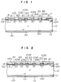
- Fig. 1 is a schematic cross-sectional view showing a termination area of a diode according to one embodiment of the present invention.
- Fig. 2 is a schematic cross-sectional view showing another embodiment of the present invention.
- Fig. 3 is a schematic cross-sectional view showing other embodiment of the present invention.
- Fig. 4 is a schematic cross-sectional view showing further embodiment of the present invention.
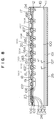
- Figs. 5A and 5B are an entire plan view and a cross-sectional view of the termination region of a pn diode prepared for investigating causes for a decrease in the breakdown voltage of a planar type, semiconductor device, respectively.
- Fig. 6 is a diagram showing results of evaluation of reverse breakdown voltages before and after high temperature, DC reverse bias tests of pn diodes with various distances between the main junction and the nearest field limiting ring region thereto as a parameter.
- Figs. 7A and 7B are diagrams illustrating a mechanism of changes in the breakdown voltage before and after high temperature, DC reverse bias tests, respectively.
- Fig. 8 is a schematic cross-sectional view showing application of the present invention to an insulated gate bipolar transistor (IGBT).
- IGBT insulated gate bipolar transistor
- Fig. 9 is a diagram showing results of high temperature, DC reverse bias tests of IGBT of Fig. 8, incorporated in a resin-sealed package, as compared with the prior art.
- Fig. 10 is a schematic circuit diagram of an inverter apparatus for controlling an electric motor comprising IGBTs and diodes according to the present invention.
- the above-mentioned object can be attained by providing a means for suppressing a decrease in the reverse breakdown voltage between the main junction and the nearest field limiting ring region to the main junction. This means will be explained in detail below.
- Figs. 5A and 5B are an entire plan view of a pn diode prepared for the tests and a cross-sectional view along the line A-A of the termination region thereof, respectively.
- a semiconductor substrate 10 having a pair of principal surfaces 11 and 12 comprises an n+ cathode layer 101 of a higher concentration, provided in contact with the principal surface 12, an n ⁇ layer 100 having a higher resistivity than that of the n+ layer 101, provided in contact with the n+ layer 101 and the other principal surface 12, a p-type anode layer 102 having a higher concentration than that of the n ⁇ layer 100 and extending from the other principal surface 12 into the n ⁇ layer 100 and forming a main junction of planar type terminating on the other principal surface 12 between the p-type anode layer 102 and the n ⁇ layer 100, a plurality of field limiting ring regions 1031-1035 of p-type having a higher concentration than that of the n ⁇ layer 100 and surrounding the p-type anode layer 102, provided at distances far from the p-type anode layer 102, and a n-type guard ring region 104 having a higher concentration than that of the n ⁇ layer 100, extending
- a cathode electrode 13 is provided in ohmic contact with the n+ cathode layer 101, an anode electrode 14 having a field plate function is provided in ohmic contact with the p-type anode layer 102, insulating layers 15 each composed of a lower layer of silicon oxide (SiO2) and an upper layer of phosphosilicate glass (PSG) are provide to cover the other principal surface 12 of the semiconductor substrate 10, field plates 161-165 are provided in contact with the field limiting ring regions 1031-1035, a field plate 17 is provided in contact with the guard ring region 104, a PSG layer 19 is provided to cover the exposed surfaces of the anode electrode 14, the insulating layers 15 and field plates 161-165 and 17, and a polyimide layer 20 is provided to cover the PSG layer 19.
- the distances from the main junction to the individual field limiting ring regions are so set that the electric fields generated below the insulating layers can be substantially equalized.
- Diodes in which the distance x between the right end of the main junction and the left end of the field limiting ring region 1031 was changed to various degrees, while making the distance d between the left end of the field limiting ring region 1031 and the left end of the guard ring region 104 constant, were prepared and incorporated into the respective ceramic packages sealed with silicone gel to measure their reverse breakdown voltages before and after a high temperature DC reverse bias test. Results are shown in Fig. 6, where the curve A shows initial breakdown voltages of diodes before the high temperature DC reverse bias test, and the larger the distance x, the higher the electric field in close proximity to the surface at the right end of the main junction, at which an avalanche breakdown takes place, resulting in a decrease in the breakdown voltage.
- line B shows breakdown voltage measurements after the high temperature, DC reverse bias test (application of reverse bias of 80% initial breakdown voltage peak at 125°C for 1,000 hours where the smaller the distance x, the higher the breakdown voltage, and there is a zone intersecting the initial breakdown voltage curve A.
- the diodes are so designed as to obtain the highest initial breakdown voltage, and thus the breakdown voltage is decreased after the high temperature, DC reverse bias test.
- DC reverse bias test is not changed from the initial breakdown voltage or larger than the initial breakdown voltage.
- the initial electric field at the end of the main junction is weak enough to balance with intensification of the electric field in that place due to the influence of plus (+) ions by the depolarization, and thus the concentration of electric fields can be relaxed.
- the breakdown voltage is not changed or becomes larger after the test.
- Minus (-) ions are gathered at the end of the guard ring region 104 and it seems that a p inversion layer 22 is formed on the surface of the n ⁇ layer 100 in close proximity to the end of the guard ring region 104, but makes it easy to extend the depletion layer in close proximity to the guard ring region 104 without any substantial influence upon changes in the breakdown voltage.
- the present invention has been established on the basis of the foregoing test results. Changes in the breakdown voltage are due to gathering of the mobile ions in the silicone gel at the end of the main junction. Since it is impossible to completely remove the mobile ions from the synthetic resin such as silicone gel, etc., it is necessary in preparation of highly reliable semiconductor devices to reduce such influences or have no such influences at all. The present invention is to meet such a necessity. Changes in the breakdown voltage in the high temperature, DC reverse bias test depend only upon the distance between the main junction and the nearest field limiting ring region to the main junction. Thus, the present invention provides a means for suppressing a decrease in the breakdown voltage between the main junction and the nearest field limiting ring region to the main junction. As shown in Fig.
- Fig. 1 is a cross-sectional view showing the termination region of a pn diode according to one embodiment of the present invention, where a semiconductor 10 having a pair of principal surfaces 11 and 12 comprises an n+ cathode layer 101 having a high concentration, provided in contact with the principal surface 11, an n ⁇ layer 100 in contact with the n+ layer 101 and the other principal surface 12 and having a higher resistivity than that of the n+ layer 101, a p-type anode layer 102 extending from the other principal surface 12 into the n ⁇ layer 100 and forming a main junction of planar type terminating on the other principal surface 12 between the n ⁇ layer 100 and the p-type anode layer 102, and having a higher concentration than that of the n ⁇ layer 100, a plurality of p-type field limiting ring regions 1031-1035, extending from the other principal surface 12 into the n ⁇ layer 100, surrounding the p-type anode layer 102 at distances far from the p-type ano
- a cathode electrode 13 is provided in ohmic contact with the n+ cathode layer 101 on the principal surface 11 of the semiconductor substrate 10
- an anode electrode 14 composed of Al ⁇ Si is provided in ohmic contact with the p-type anode layer 102 on the other principal surface 12 of the semiconductor substrate 10
- insulating layers 15, each comprising a silicon oxide (SiO2) layer as a lower layer and a phosphosilicate glass (PSG) layer as an upper layer are provided to cover the regions with no formation of anode electrode on the other principal surface 12 of the semiconductor substrate 10
- field plates 162-165, composed of Al ⁇ Si, each of whose ends extends over the boundary between the respective field limiting ring regions and the n ⁇ layer 100 over the insulating layer 15 are provided in contact with other field limiting ring regions 1032-1035 than the nearest one to the p-type anode layer 102
- another field plate 17, composed of Al ⁇ Si, whose end extends over the boundary between the guard
- the conduction layer 18 in an electrically floating state can be formed from the common material (Al ⁇ Si) by the common steps to those for the field plates 162-165 or from polycrystalline silicon usually used in the semiconductor production technique, the conduction layer can be produced by very simple means and thus is suitable for effective mass production.
- the conduction layer 18 is only between the main junction and the nearest field limiting ring region 1031 thereto, as mentioned above. Since the conduction layer 18 is partially at a higher potential than that on the surface of the n ⁇ layer 100 just below the conduction layer 18, there may be a new problem, depending upon a potential difference therebetween. When the potential difference is small, there will be no problem at all, but when the potential difference is large, hot carriers generated on the surface of the n ⁇ layer are attracted to the electric field of the conduction layer 18 and plunged into the insulating layer 15, resulting in deterioration of the insulating layer 15 with time to change the reverse breakdown voltage.
- the conduction layer 18 is provided only between the main junction and the nearest field limiting ring region 1031 thereto, there will be no such a new problem substantially, because of a small potential difference, but when such conduction layers are provided also between the adjacent field limiting ring region, the problem is remarkable. Thus, it is preferable to provide the conduction layer at the above-mentioned position.
- the present invention directed to a diode has been described in the foregoing, but the present invention can be applied also to other semiconductor devices than the diode.
- the present invention is applied to other semiconductor devices than the diode, only the region for forming the main junction can be changed, while retaining the termination region as unchanged.
- an n emitter layer is formed in the p-type anode layer 102, while changing the anode electrode 14 to a base electrode and the cathode electrode 13 to a collector electrode, and an emitter electrode is provided on the n emitter layer.
- an n emitter layer is formed in the p-type anode layer 102, while changing the n+ cathode layer to a p+ layer, the anode electrode 14 to a gate electrode, and the cathode electrode 13 to an anode electrode, and a cathode electrode is provided on the n emitter layer.
- an n source layer is formed in the p-type anode layer 102, a source electrode is provided on the n source layer, an insulating gate is provided from the n ⁇ layer 100 to the n source layer, and the cathode electrode is changed to a drain electrode.
- a p+ layer is provided between the n+ cathode layer and the drain electrode in MOSFET.
- Fig. 2 is a cross-sectional view of a termination region according to another embodiment of the present invention. Differences from the embodiment shown in Fig. 1 are that a field plate 161 is formed also in the nearest field limiting ring region 1031 to the main junction in the same manner as in other field limiting ring regions in place of the conduction layer 18, and an n layer 105 having a higher concentration than that of the n ⁇ layer 100 is provided on the surface of the n ⁇ layer 100 between the main junction and the nearest field limiting ring region 1031 thereto.
- the n layer 105 is formed in advance in the region where an accumulation layer (high concentration n-type) is formed due to the influence of mobile ions in the n ⁇ layer 100, and thus there will be no substantial influence by mobile ions. That is, the depletion layer extending from the main junction is made hard to extend on the surface of the n layer 105 and easy to extend within the n ⁇ layer 100 in advance, and thus potential transfer into the field limiting ring region 1031 is made to take place within the n ⁇ layer 100 not susceptible to the influence by the accumulation layer. Thus, if the impurity concentration of the n layer 105 is too high, the initial breakdown voltage will be decreased, whereas, if it is too low, the effect of the present invention will not be obtained.
- the concentration is desirable to make the concentration equal to or by about one order higher than the amount of electrons (the amount of electrons in the accumulation layer) induced on the surface of the n ⁇ layer 100 by mobile ions. Since the amount of electrons in the accumulation layer has been estimated to be in the order of 1011/cm2 by tests, it is preferably in the order of about 1012/cm2. In order to make the depletion layer easy to extend within the n ⁇ layer 100, it is preferable that the n layer 105 has as small a depth as possible. Furthermore, it is preferable to provide the n layer 105 only between the main junction and the nearest field limiting ring region 1031 thereto, as in this embodiment.
- the n layer 105 acts to suppress the extension of the depletion layer at least on the surface between the main junction and the nearest field limiting ring region 1031 thereto, (that is, to strengthen the electric field), and the degree of suppression depends upon the impurity concentration and depth of the n layer 105.
- Fig. 3 is a cross-sectional view of a termination area according to other embodiment of the present invention. Differences from the embodiment shown in Fig. 1 are that a field plate 161 is provided in the nearest field limiting ring region 1031 to the main junction and is extended to the p-type anode layer 102 through the insulating layer 15 in place of the conduction layer 18. According to this structure, the field plate 161 is fixed to the higher potential of the field limiting ring region 1031 than that of the main junction, when the main junction is in a reverse bias state. Thus, electrons are induced to gather on the surface of the n ⁇ layer 100 just below the field plate 161 to form an accumulation layer. Thus, the same effect as in the embodiment of providing the n layer 105 in advance, as shown in Fig. 2, can be obtained, and the depletion layer is easier to extend inside the n ⁇ layer 100 than on the surface thereof.
- the field plate 161 of this Example only between the main junction and the nearest field limiting ring region 1031 thereto.
- the field plate 161 has a higher potential than that on the surface of the n ⁇ layer 100 just below the field plate 161, and thus there may be a new problem due to a potential difference therebetween.
- a small potential difference there will be no problem at all, whereas in case of a larger potential difference hot carriers generated on the surface of n ⁇ layer 100 are attracted to the electric field of field plate 161 and plunged into the insulating layer 15, resulting in deterioration of the insulating film 15 with time to change the reverse breakdown voltage.
- the field plate 161 When the field plate 161 is provided only between the main junction and the nearest field limiting ring region thereto, there will be no problem substantially, because of a small potential difference, but when such field plates are provided between the adjacent field limiting ring regions there will be a problem. Thus, it is preferable to provide the field plate 161 only between the main junction and the nearest field limiting region 1031 thereto, as explained above. In order to make the potential difference smaller, it is preferable that the distance between the main junction and the field limiting region 1031 is as small as possible.
- Fig. 4 is a cross-sectional view of a termination region according to further embodiment of the present invention. Differences from the embodiment of Fig. 1 are that field plates 160 and 161 are formed on the p-type anode layer 102 and the nearest field limiting ring region to the main junction, respectively, and the field limiting ring region has a projection 1031a at the bottom, protruded toward the main junction. According to this structure, the projection 1031a is formed below the region, where an accumulation layer (high concentration n-type) is formed due to the influence by mobile ions, and thus the influence by mobile ions can be made substantially free.
- an accumulation layer high concentration n-type
- the depletion layer extending from the main function can readily reach the projection 1031a provided inside the n ⁇ layer 100 without any influence by the surface state of the n ⁇ layer 100, and thus the potential transfer into the field limiting ring region 1031 can be minimized to such a degree that the influence by an accumulation layer formed on the surface of the n ⁇ layer 100 by mobile ions can be disregarded.
- changes in the breakdown voltage can be suppressed by a simple means and thus highly reliable, planar type semiconductor devices of high breakdown voltage suitable for mass-production can be produced.
- extension of the depletion layer can be made easier inside the n ⁇ layer 100 than on the surface thereof, and thus this embodiment is the same as embodiments shown in Figs. 2 and 3 in principle. That is, the effect of the present invention can be obtained even by a combination of these means.
- Fig. 8 is a cross-sectional view showing application of the present invention to an insulated gate bipolar transistor (IGBT), whose structure comprises, as explained referring to Fig. 1, n source layers 106 formed in a p-type anode layer 102 of Fig. 1, a source electrode 23 provided on the n source electrodes 106, an insulating gate 24 extending from the n ⁇ layer 100 to the n source layers provided on the n ⁇ layer 100, a collector electrode 25 changed from the cathode electrode, and a p+ layer 107 provided between the n+ cathode layer 101 and the collector electrode 25.
- IGBT insulated gate bipolar transistor
- the insulating gate comprises a gate oxide layer 241 composed of SiO2, a gate electrode 242 composed of polycrystalline silicon doped with phosphorus at a high concentration and an insulating layer 243 composed of PSG, provided to cover the gate electrode 242.
- the source electrode 23 is in contact not only with the n source layers 106, but also with the p-type anode layer 102.
- the potential of the conduction layer 18 is fixed to an intermediate potential between the main junction and the field limiting ring region 1031 and plays a role of shield effect, and thus there are no influences by external factors such as mobile ions, etc. at all.
- Fig. 9 shows results of high temperature, DC reverse bias tests of IGBT of Fig. 8, incorporated in a resin-sealed package, as compared with the prior art without the conduction layer 18.
- the breakdown voltage is considerably decreased after a few ten hours, whereas according to the present invention the breakdown voltage is not changed at all even after 1,000 hours. That is, a very highly reliable IGBT of high breakdown voltage can be produced.
- a higher breakdown voltage of semiconductor devices having a planar junction can be easily attained according to the present invention, and thus a power transducer can have a higher reliability and a higher capacity.
- Fig. 10 shows one embodiment of the structure of an inverter apparatus for controlling an electric motor using IGBTs and diodes according to the present invention, where a voltage type, inverter circuit is made with 6 IGBTs to control a three-phase induction motor 30.
- Its unit circuit comprises an IGBT 31, a fly-wheel diode (FD) 32, a snubber diode (SD) 33, a snubber resistor (SR) 34, and a snubber condenser (SC) 35.
- IGBT itself is a device with a high switching speed, and by application of the present invention thereto IGBT and likewise diodes can have a higher reverse breakdown voltage.
- Such IGBTs and diodes even if used for a long time, are not susceptible to a decrease in the breakdown voltage and thus an inverter apparatus can have a larger capacity with a higher frequency and with a high reliability.
- the present invention is effective for smaller size, lighter weight, lower loss, lower noise, etc. of an inverter apparatus, and a lower cost and a higher efficiency of a system using an inverter system can be attained according to the present invention.
- a planar junction without any decrease in the reverse breakdown voltage can be obtained even if used for a long time, and a highly reliable semiconductor devices of high breakdown voltage can be readily and effectively produced.
Landscapes
- Engineering & Computer Science (AREA)
- Power Engineering (AREA)
- Microelectronics & Electronic Packaging (AREA)
- Condensed Matter Physics & Semiconductors (AREA)
- General Physics & Mathematics (AREA)
- Physics & Mathematics (AREA)
- Computer Hardware Design (AREA)
- Ceramic Engineering (AREA)
- Manufacturing & Machinery (AREA)
- Electrodes Of Semiconductors (AREA)
- Thyristors (AREA)
- Bipolar Transistors (AREA)
- Bipolar Integrated Circuits (AREA)
Abstract
Description
- The present invention relates to a semiconductor device, and more particularly to a semiconductor device with a planar junction suitable for higher reliability of reverse breakdown characteristics.
- Development of semiconductor devices having a higher reverse breakdown voltage has been desired due to a demand for larger capacity for inverter apparatuses, etc. Generally, the reverse breakdown voltage of a semiconductor device depends substantially upon the pn junction-terminating region, and production of semiconductor devices with a higher breakdown voltage depends on a termination technique to uniformly weaken the electric field in this region. Heretofore, a mesa type semiconductor devices have been usually employed as a termination technique for higher breakdown voltage. However, production of the mesa type semiconductor devices requires complicated steps such as bevel formation, resin coating onto the bevel regions, etc. and also requires a large area for the bevel regions, and thus is not suitable for mass production. Recently, relatively small semiconductor devices of chip size with pn junction terminals of planar type, that is, the so called planar type semiconductor devices, have been employed. The planar type semiconductor device is to distribute an electric field applied to the main junction in the planar direction, thereby relaxing a local electric field concentration. For this purpose, a procedure for providing a plurality of field limiting ring regions to surround the main junction has been found suitable for mass production because of simple production steps and has been widely applied to devices having a relative low breakdown voltage. When the distances between the field limiting ring regions are so set that the electric field may not be unevenly distributed, there is a possibility to obtain devices of stable, high breakdown voltage characteristic.
- The case of providing field limiting ring regions has the following problems and no stable, high breakdown voltage characteristics have been obtained so far. A first problem is occurrence of uneven distribution of electric field in close proximity to the interface due to influences of fixed charge, etc. at the interface between the silicon substrate and the silicon oxide layer, and the degree of distribution fluctuates due to production factors. Relatively stable, high breakdown voltage can be obtained only as the initial characteristics by an improved technique of forming a better silicon oxide layer or by stabilization of the interface by hydrogen treatment. A second problem is a decrease in the breakdown voltage in a reliability test, typically a high temperature DC reverse bias test. Its cause seems to be due to influences of charged particles introduced therein or attached thereto from the outside of semiconductor devices. Generally, semiconductor devices of high breakdown voltage are employed after having been sealed with a synthetic resin such as a silicon-gel, etc. to prevent electric discharge or introduction of moisture, and in case of synthetic resin sealing the decrease in the breakdown voltage is very remarkable. The higher the resistivity of a silicon substrate, that is, the higher the breakdown voltage of a planar type semiconductor device, the more remarkable occurrence of such a phenomenon. Thus, it has been the important task in practical applications of planar type semiconductor devices of high breakdown voltage to solve these problems.
- For example, a structure is proposed to meet this task in JP-B-52-27032, where the main junction is connected to the field limiting ring region by a conduction layer having a high resistivity and a shunt current is passed through the conduction layer on the basis of the reverse breakdown voltage and equalizing the surface potential distribution in the termination region to stabilize the semiconductor surface. Decrease in the breakdown voltage in the high temperature, reverse bias test can be prevented with this structure.
- The conduction layer of the above-mentioned prior art requires a resistivity as high as about 10⁷ to about 10¹⁰ Ω, and usually an oxygen-doped or nitrogen-doped polysilicon layer is used as the layer of high resistivity, but is not suitable for the mass production due to very difficult control of the resistivity. Furthermore, since the shunt current is passed on the basis of the reverse breakdown voltage, the conduction layer of the prior art has a problem such as essentially large reverse breakdown current and such unstable factors that the current level depends also upon the resistivity of the conduction layer, and so forth.
- An object of the present invention is to provide a semiconductor device having a highly reliable planar junction of high breakdown voltage, where influences by external factors such as charged particles, etc. are suppressed by a simple means.
- The present semiconductor device for attaining the above-mentioned object is characterized in that the semiconductor device comprises a main junction exposed to the principal surface of a semiconductor substrate, a plurality of field limiting ring regions surrounding the main junction, and a means for suppressing a decrease in the reverse breakdown voltage provided between the main junction and the nearest field limiting ring region to the main junction.
- The means for suppressing a decrease in the reverse breakdown voltage includes (1) to make the distance between the main junction and the nearest field limiting ring region to the main junction smaller than the distance between the adjacent field limiting ring regions, (2) to provide a conduction layer in an electrically floating state between the main junction and the nearest field limiting ring region to the main junction through an insulating layer, (3) to provide a region having the same conduction type as that of the substrate and having a higher impurity concentration than that of the substrate on the surface of the semiconductor substrate between the main junction and the nearest field limiting ring region to the main junction, (4) to make the distance between the main junction and the nearest field limiting ring region to the main junction smaller inside the semiconductor substrate than that on the principal surface of the semiconductor substrate, (5) to cover the surface of the semiconductor substrate between the main junction and the nearest field limiting ring region to the main junction with a conduction layer through an insulating layer and electrically connect the conduction layer to the nearest field limiting ring region to the main junction, or similar means to those mentioned above.
- Fig. 1 is a schematic cross-sectional view showing a termination area of a diode according to one embodiment of the present invention.
- Fig. 2 is a schematic cross-sectional view showing another embodiment of the present invention.
- Fig. 3 is a schematic cross-sectional view showing other embodiment of the present invention.
- Fig. 4 is a schematic cross-sectional view showing further embodiment of the present invention.
- Figs. 5A and 5B are an entire plan view and a cross-sectional view of the termination region of a pn diode prepared for investigating causes for a decrease in the breakdown voltage of a planar type, semiconductor device, respectively.
- Fig. 6 is a diagram showing results of evaluation of reverse breakdown voltages before and after high temperature, DC reverse bias tests of pn diodes with various distances between the main junction and the nearest field limiting ring region thereto as a parameter.
- Figs. 7A and 7B are diagrams illustrating a mechanism of changes in the breakdown voltage before and after high temperature, DC reverse bias tests, respectively.
- Fig. 8 is a schematic cross-sectional view showing application of the present invention to an insulated gate bipolar transistor (IGBT).
- Fig. 9 is a diagram showing results of high temperature, DC reverse bias tests of IGBT of Fig. 8, incorporated in a resin-sealed package, as compared with the prior art.
- Fig. 10 is a schematic circuit diagram of an inverter apparatus for controlling an electric motor comprising IGBTs and diodes according to the present invention.
- According to the present invention, the above-mentioned object can be attained by providing a means for suppressing a decrease in the reverse breakdown voltage between the main junction and the nearest field limiting ring region to the main junction. This means will be explained in detail below.
- In order to investigate causes for a decrease in the breakdown voltage of semiconductor devices having a planar junction, the present inventors have conducted tests and have clarified their detailed mechanism.
- Figs. 5A and 5B are an entire plan view of a pn diode prepared for the tests and a cross-sectional view along the line A-A of the termination region thereof, respectively.
- A
semiconductor substrate 10 having a pair ofprincipal surfaces 11 and 12 comprises an n⁺cathode layer 101 of a higher concentration, provided in contact with theprincipal surface 12, an n⁻layer 100 having a higher resistivity than that of the n⁺layer 101, provided in contact with the n⁺layer 101 and the otherprincipal surface 12, a p-type anode layer 102 having a higher concentration than that of the n⁻layer 100 and extending from the otherprincipal surface 12 into the n⁻layer 100 and forming a main junction of planar type terminating on the otherprincipal surface 12 between the p-type anode layer 102 and the n⁻layer 100, a plurality of field limiting ring regions 1031-1035 of p-type having a higher concentration than that of the n⁻layer 100 and surrounding the p-type anode layer 102, provided at distances far from the p-type anode layer 102, and a n-typeguard ring region 104 having a higher concentration than that of the n⁻layer 100, extending from the otherprincipal surface 12 into the n⁻layer 100, provided at the periphery of the otherprincipal surface 12. Acathode electrode 13 is provided in ohmic contact with the n⁺cathode layer 101, ananode electrode 14 having a field plate function is provided in ohmic contact with the p-type anode layer 102,insulating layers 15 each composed of a lower layer of silicon oxide (SiO₂) and an upper layer of phosphosilicate glass (PSG) are provide to cover the otherprincipal surface 12 of thesemiconductor substrate 10, field plates 161-165 are provided in contact with the field limiting ring regions 1031-1035, afield plate 17 is provided in contact with theguard ring region 104, aPSG layer 19 is provided to cover the exposed surfaces of theanode electrode 14, theinsulating layers 15 and field plates 161-165 and 17, and apolyimide layer 20 is provided to cover thePSG layer 19. The distances from the main junction to the individual field limiting ring regions are so set that the electric fields generated below the insulating layers can be substantially equalized. - Diodes, in which the distance x between the right end of the main junction and the left end of the field limiting
ring region 1031 was changed to various degrees, while making the distance d between the left end of the field limitingring region 1031 and the left end of theguard ring region 104 constant, were prepared and incorporated into the respective ceramic packages sealed with silicone gel to measure their reverse breakdown voltages before and after a high temperature DC reverse bias test. Results are shown in Fig. 6, where the curve A shows initial breakdown voltages of diodes before the high temperature DC reverse bias test, and the larger the distance x, the higher the electric field in close proximity to the surface at the right end of the main junction, at which an avalanche breakdown takes place, resulting in a decrease in the breakdown voltage. When the distance x is too small on the other hand, a voltage load on the field limiting ring regions 1032-1035 existing at the outside of the field limitingring region 1031 is larger, and thus concentration of the electric field takes place at the right end of any of the field limiting ring regions 1031-1035, resulting in a decrease in the breakdown voltage. That is, there is an optimum distance x at which the highest breakdown voltage is obtainable. - On the other hand, line B shows breakdown voltage measurements after the high temperature, DC reverse bias test (application of reverse bias of 80% initial breakdown voltage peak at 125°C for 1,000 hours where the smaller the distance x, the higher the breakdown voltage, and there is a zone intersecting the initial breakdown voltage curve A. Usually, the diodes are so designed as to obtain the highest initial breakdown voltage, and thus the breakdown voltage is decreased after the high temperature, DC reverse bias test. However, such a very interesting fact has been found that there is a point at which the breakdown voltage after the high temperature, DC reverse bias test is not changed from the initial breakdown voltage or larger than the initial breakdown voltage. As a result of detailed study of causes for this fact, it has been found that the phenomena of decrease in the breakdown voltage after the high temperature, DC reverse bias test appear on the bias of mechanism shown in Figs. 7A and 7B. The mechanism is as follows:
As shown in Fig. 7A, peak electric fields generated at the ends of the individual field limiting ring regions are substantially equally distributed before the test because the distances between the adjacent regions are so set that no uneven distribution of electric fields may take place, but mobile ions in the silicone gel travel by a potential on the surface of the insulating layer, thereby occasioning polarization. Plus (+) ions are moved to the end of the main junction at the lowest potential, and anaccumulation layer 21 is formed on the surface of n⁻layer 100 between the main junction and the field limitingring region 1031 due to the generated charge. Thus, the depletion layer is hard to extend (which is equivalent to substantial extension of the distance x between the main junction and the field limiting ring region 1031), and thus the electric fields are concentrated on the end of the main junction, resulting in a decrease in the breakdown voltage (Fig. 7B). - When the distance x is smaller than the optimum distance as to the initial breakdown voltage on the other hand, the initial electric field at the end of the main junction is weak enough to balance with intensification of the electric field in that place due to the influence of plus (+) ions by the depolarization, and thus the concentration of electric fields can be relaxed. As a result, the breakdown voltage is not changed or becomes larger after the test. Minus (-) ions are gathered at the end of the
guard ring region 104 and it seems thata p inversion layer 22 is formed on the surface of the n⁻layer 100 in close proximity to the end of theguard ring region 104, but makes it easy to extend the depletion layer in close proximity to theguard ring region 104 without any substantial influence upon changes in the breakdown voltage. - The present invention has been established on the basis of the foregoing test results. Changes in the breakdown voltage are due to gathering of the mobile ions in the silicone gel at the end of the main junction. Since it is impossible to completely remove the mobile ions from the synthetic resin such as silicone gel, etc., it is necessary in preparation of highly reliable semiconductor devices to reduce such influences or have no such influences at all. The present invention is to meet such a necessity. Changes in the breakdown voltage in the high temperature, DC reverse bias test depend only upon the distance between the main junction and the nearest field limiting ring region to the main junction. Thus, the present invention provides a means for suppressing a decrease in the breakdown voltage between the main junction and the nearest field limiting ring region to the main junction. As shown in Fig. 6, it is one of the effective means to make the distance between the main junction and the nearest field limiting ring region to the main junction approach such a distance at which an equal breakdown voltage after the high temperature, DC reverse bias test to the initial breakdown voltage can be obtained. Highly reliable semiconductor devices of planar junction can be obtained by this very simple means.
- It is not preferable to narrow the other distances between the adjacent field limiting ring regions than that between the main junction and the nearest field limiting ring region to the main junction, because the narrowing gives rise to uneven distribution of the electric fields. In order to narrow the distances between the adjacent field limiting ring regions without any uneven distribution of electric fields, all the distances between the adjacent field limiting ring regions must be evenly narrowed and also the number of the field limiting ring regions must be increased. This leads to an increase in the area of termination region, resulting in an increase in the chip area and a decrease in the production yield. Thus, it is only desirable to narrow the distance between the main junction and the nearest field limiting ring region to the main junction rather than the distances between the adjacent field limiting ring regions.
- The present invention will be described in detail below, referring to drawings illustrating the embodiments of the present invention.
- Fig. 1 is a cross-sectional view showing the termination region of a pn diode according to one embodiment of the present invention, where a semiconductor 10 having a pair of principal surfaces 11 and 12 comprises an n⁺ cathode layer 101 having a high concentration, provided in contact with the principal surface 11, an n⁻ layer 100 in contact with the n⁺ layer 101 and the other principal surface 12 and having a higher resistivity than that of the n⁺ layer 101, a p-type anode layer 102 extending from the other principal surface 12 into the n⁻ layer 100 and forming a main junction of planar type terminating on the other principal surface 12 between the n⁻ layer 100 and the p-type anode layer 102, and having a higher concentration than that of the n⁻ layer 100, a plurality of p-type field limiting ring regions 1031-1035, extending from the other principal surface 12 into the n⁻ layer 100, surrounding the p-type anode layer 102 at distances far from the p-type anode 102 and having a higher concentration than that of the n⁻ layer 100, and an n-type guard ring region extending from the other principal surface 12 into the n⁻ layer 100 at the periphery of the other principal surface 12 and having a higher concentration than that of the n⁻ layer 100. A
cathode electrode 13 is provided in ohmic contact with the n⁺cathode layer 101 on the principal surface 11 of thesemiconductor substrate 10, ananode electrode 14 composed of Aℓ·Si is provided in ohmic contact with the p-type anode layer 102 on the otherprincipal surface 12 of thesemiconductor substrate 10, insulatinglayers 15, each comprising a silicon oxide (SiO₂) layer as a lower layer and a phosphosilicate glass (PSG) layer as an upper layer are provided to cover the regions with no formation of anode electrode on the otherprincipal surface 12 of thesemiconductor substrate 10, field plates 162-165, composed of Aℓ·Si, each of whose ends extends over the boundary between the respective field limiting ring regions and the n⁻layer 100 over the insulatinglayer 15 are provided in contact with other field limiting ring regions 1032-1035 than the nearest one to the p-type anode layer 102, anotherfield plate 17, composed of Aℓ·Si, whose end extends over the boundary between theguard ring region 104 and the n⁻layer 100 over the insulatinglayer 15 is provided in contact with theguard ring region 104, an electrically floatingconduction layer 18, composed of Si·Aℓ, extending from the p-type anode layer 102 to the nearest field limitingring region 1031 thereto is provided on the insulatinglayer 15, aPSG layer 19 is provided to cover exposed parts of theanode electrode 14, the insulatinglayers 15, the field plates 162-165 and 17 and theconduction layer 15, and apolyimide layer 20 is provided to cover thePSG layer 19. - When a polarity of making the main junction take a reverse bias (a higher potential at the
cathode electrode 13 than at the anode electrode 14) is applied between theanode electrode 14 and thecathode electrode 13 in the pn diode with the above-mentioned structure, the potential of theconduction layer 18 is fixed to an intermediate potential between the main junction and the nearest field limitingring region 1031 thereto to play a role of shield effect, and thus the pn diode has no influences by external factors such as mobile ions, etc. at all. Thus, no changes occur at all in the breakdown voltage before and after the high temperature, DC bias test of resin-sealed diode devices, and thus a very reliable planar type diodes of high breakdown voltage can be produced. Since theconduction layer 18 in an electrically floating state can be formed from the common material (Aℓ·Si) by the common steps to those for the field plates 162-165 or from polycrystalline silicon usually used in the semiconductor production technique, the conduction layer can be produced by very simple means and thus is suitable for effective mass production. - It is preferable to provide the
conduction layer 18 only between the main junction and the nearest field limitingring region 1031 thereto, as mentioned above. Since theconduction layer 18 is partially at a higher potential than that on the surface of the n⁻layer 100 just below theconduction layer 18, there may be a new problem, depending upon a potential difference therebetween. When the potential difference is small, there will be no problem at all, but when the potential difference is large, hot carriers generated on the surface of the n⁻ layer are attracted to the electric field of theconduction layer 18 and plunged into the insulatinglayer 15, resulting in deterioration of the insulatinglayer 15 with time to change the reverse breakdown voltage. When theconduction layer 18 is provided only between the main junction and the nearest field limitingring region 1031 thereto, there will be no such a new problem substantially, because of a small potential difference, but when such conduction layers are provided also between the adjacent field limiting ring region, the problem is remarkable. Thus, it is preferable to provide the conduction layer at the above-mentioned position. - The embodiment of the present invention directed to a diode has been described in the foregoing, but the present invention can be applied also to other semiconductor devices than the diode. When the present invention is applied to other semiconductor devices than the diode, only the region for forming the main junction can be changed, while retaining the termination region as unchanged. For example, in case of a bipolar transistor, an n emitter layer is formed in the p-
type anode layer 102, while changing theanode electrode 14 to a base electrode and thecathode electrode 13 to a collector electrode, and an emitter electrode is provided on the n emitter layer. - In case of a thyristor, an n emitter layer is formed in the p-
type anode layer 102, while changing the n⁺ cathode layer to a p⁺ layer, theanode electrode 14 to a gate electrode, and thecathode electrode 13 to an anode electrode, and a cathode electrode is provided on the n emitter layer. - In case of MOSFET, an n source layer is formed in the p-
type anode layer 102, a source electrode is provided on the n source layer, an insulating gate is provided from the n⁻layer 100 to the n source layer, and the cathode electrode is changed to a drain electrode. - In case of an insulated gate dipolar transistor (IGBT) a p⁺ layer is provided between the n⁺ cathode layer and the drain electrode in MOSFET.
- Fig. 2 is a cross-sectional view of a termination region according to another embodiment of the present invention. Differences from the embodiment shown in Fig. 1 are that a
field plate 161 is formed also in the nearest field limitingring region 1031 to the main junction in the same manner as in other field limiting ring regions in place of theconduction layer 18, and an n layer 105 having a higher concentration than that of the n⁻layer 100 is provided on the surface of the n⁻layer 100 between the main junction and the nearest field limitingring region 1031 thereto. According to this structure, the n layer 105 is formed in advance in the region where an accumulation layer (high concentration n-type) is formed due to the influence of mobile ions in the n⁻layer 100, and thus there will be no substantial influence by mobile ions. That is, the depletion layer extending from the main junction is made hard to extend on the surface of the n layer 105 and easy to extend within the n⁻layer 100 in advance, and thus potential transfer into the field limitingring region 1031 is made to take place within the n⁻layer 100 not susceptible to the influence by the accumulation layer. Thus, if the impurity concentration of the n layer 105 is too high, the initial breakdown voltage will be decreased, whereas, if it is too low, the effect of the present invention will not be obtained. It is desirable to make the concentration equal to or by about one order higher than the amount of electrons (the amount of electrons in the accumulation layer) induced on the surface of the n⁻layer 100 by mobile ions. Since the amount of electrons in the accumulation layer has been estimated to be in the order of 10¹¹/cm² by tests, it is preferably in the order of about 10¹²/cm². In order to make the depletion layer easy to extend within the n⁻layer 100, it is preferable that the n layer 105 has as small a depth as possible. Furthermore, it is preferable to provide the n layer 105 only between the main junction and the nearest field limitingring region 1031 thereto, as in this embodiment. - As explained above, the n layer 105 acts to suppress the extension of the depletion layer at least on the surface between the main junction and the nearest field limiting
ring region 1031 thereto, (that is, to strengthen the electric field), and the degree of suppression depends upon the impurity concentration and depth of the n layer 105. Thus, it is not preferable to provide the n layer 105 at other positions than the position between the main junction and the nearest field limitingring region 1031 thereto, because such a provision is a factor for causing fluctuations in the production steps, thereby changing the initial breakdown voltage largely. - According to this embodiment changes in the breakdown voltage can be suppressed by a very simple means without fail, and thus highly reliable, planar type semiconductor devices of high breakdown voltage suitable for mass production can be produced.
- Fig. 3 is a cross-sectional view of a termination area according to other embodiment of the present invention. Differences from the embodiment shown in Fig. 1 are that a
field plate 161 is provided in the nearest field limitingring region 1031 to the main junction and is extended to the p-type anode layer 102 through the insulatinglayer 15 in place of theconduction layer 18. According to this structure, thefield plate 161 is fixed to the higher potential of the field limitingring region 1031 than that of the main junction, when the main junction is in a reverse bias state. Thus, electrons are induced to gather on the surface of the n⁻layer 100 just below thefield plate 161 to form an accumulation layer. Thus, the same effect as in the embodiment of providing the n layer 105 in advance, as shown in Fig. 2, can be obtained, and the depletion layer is easier to extend inside the n⁻layer 100 than on the surface thereof. - It is preferable to provide the
field plate 161 of this Example only between the main junction and the nearest field limitingring region 1031 thereto. As explained above, thefield plate 161 has a higher potential than that on the surface of the n⁻layer 100 just below thefield plate 161, and thus there may be a new problem due to a potential difference therebetween. In case of a small potential difference there will be no problem at all, whereas in case of a larger potential difference hot carriers generated on the surface of n⁻layer 100 are attracted to the electric field offield plate 161 and plunged into the insulatinglayer 15, resulting in deterioration of the insulatingfilm 15 with time to change the reverse breakdown voltage. When thefield plate 161 is provided only between the main junction and the nearest field limiting ring region thereto, there will be no problem substantially, because of a small potential difference, but when such field plates are provided between the adjacent field limiting ring regions there will be a problem. Thus, it is preferable to provide thefield plate 161 only between the main junction and the nearestfield limiting region 1031 thereto, as explained above. In order to make the potential difference smaller, it is preferable that the distance between the main junction and thefield limiting region 1031 is as small as possible. - Fig. 4 is a cross-sectional view of a termination region according to further embodiment of the present invention. Differences from the embodiment of Fig. 1 are that
field plates type anode layer 102 and the nearest field limiting ring region to the main junction, respectively, and the field limiting ring region has a projection 1031a at the bottom, protruded toward the main junction. According to this structure, the projection 1031a is formed below the region, where an accumulation layer (high concentration n-type) is formed due to the influence by mobile ions, and thus the influence by mobile ions can be made substantially free. That is, when the main junction is in a reverse bias state, the depletion layer extending from the main function can readily reach the projection 1031a provided inside the n⁻layer 100 without any influence by the surface state of the n⁻layer 100, and thus the potential transfer into the field limitingring region 1031 can be minimized to such a degree that the influence by an accumulation layer formed on the surface of the n⁻layer 100 by mobile ions can be disregarded. According to the present invention, changes in the breakdown voltage can be suppressed by a simple means and thus highly reliable, planar type semiconductor devices of high breakdown voltage suitable for mass-production can be produced. In this embodiment, extension of the depletion layer can be made easier inside the n⁻layer 100 than on the surface thereof, and thus this embodiment is the same as embodiments shown in Figs. 2 and 3 in principle. That is, the effect of the present invention can be obtained even by a combination of these means. - Fig. 8 is a cross-sectional view showing application of the present invention to an insulated gate bipolar transistor (IGBT), whose structure comprises, as explained referring to Fig. 1, n source layers 106 formed in a p-
type anode layer 102 of Fig. 1, asource electrode 23 provided on then source electrodes 106, an insulatinggate 24 extending from the n⁻layer 100 to the n source layers provided on the n⁻layer 100, acollector electrode 25 changed from the cathode electrode, and a p⁺layer 107 provided between the n⁺cathode layer 101 and thecollector electrode 25. The insulating gate comprises agate oxide layer 241 composed of SiO₂, agate electrode 242 composed of polycrystalline silicon doped with phosphorus at a high concentration and an insulating layer 243 composed of PSG, provided to cover thegate electrode 242. Thesource electrode 23 is in contact not only with the n source layers 106, but also with the p-type anode layer 102. When a voltage of making the main junction into a reverse bias state is applied between thesource electrode 23 and thecollector electrode 25 in this structure, the potential of theconduction layer 18 is fixed to an intermediate potential between the main junction and the field limitingring region 1031 and plays a role of shield effect, and thus there are no influences by external factors such as mobile ions, etc. at all. - Fig. 9 shows results of high temperature, DC reverse bias tests of IGBT of Fig. 8, incorporated in a resin-sealed package, as compared with the prior art without the
conduction layer 18. According to the prior art, the breakdown voltage is considerably decreased after a few ten hours, whereas according to the present invention the breakdown voltage is not changed at all even after 1,000 hours. That is, a very highly reliable IGBT of high breakdown voltage can be produced. - As explained above, a higher breakdown voltage of semiconductor devices having a planar junction can be easily attained according to the present invention, and thus a power transducer can have a higher reliability and a higher capacity.
- Fig. 10 shows one embodiment of the structure of an inverter apparatus for controlling an electric motor using IGBTs and diodes according to the present invention, where a voltage type, inverter circuit is made with 6 IGBTs to control a three-
phase induction motor 30. Its unit circuit comprises an IGBT 31, a fly-wheel diode (FD) 32, a snubber diode (SD) 33, a snubber resistor (SR) 34, and a snubber condenser (SC) 35. IGBT itself is a device with a high switching speed, and by application of the present invention thereto IGBT and likewise diodes can have a higher reverse breakdown voltage. Such IGBTs and diodes, even if used for a long time, are not susceptible to a decrease in the breakdown voltage and thus an inverter apparatus can have a larger capacity with a higher frequency and with a high reliability. Thus, the present invention is effective for smaller size, lighter weight, lower loss, lower noise, etc. of an inverter apparatus, and a lower cost and a higher efficiency of a system using an inverter system can be attained according to the present invention. - According to the present invention, a planar junction without any decrease in the reverse breakdown voltage can be obtained even if used for a long time, and a highly reliable semiconductor devices of high breakdown voltage can be readily and effectively produced.
Claims (11)
- A semiconductor device, characterized in comprising a semiconductor substrate (10), to one principal surface (12) of which a first semiconductor region (100) of first conduction type is exposed, a second semiconductor region (102) of second conduction type extending from the principal surface (12) into the first semiconductor region (100) and forming a pn junction with the first semiconductor region (100) being provided on the principal surface (12), and a plurality of third annular semiconductor regions (1031-1038) of second conduction type extending from the principal surface (12) into the first semiconductor region (100) and surrounding the second semiconductor region (102) being provided distant from the second semiconductor region (102) and on the principal surface (12), wherein a means for suppressing a reduction of reverse breakdown voltage is provided between the second semiconductor region (102) and the nearest third annular semiconductor region (1031) to the second semiconductor region (102).
- A semiconductor device, which comprises a semiconductor substrate (10), to one principal surface (12) of which a first semiconductor region (100) of first conduction type is exposed, a second semiconductor region (102) of second conduction type extending from the principal surface (12) into the first semiconductor region (100) and forming a pn junction with the first semiconductor region (100) being provided on the principal surface (12), and a plurality of third annular semiconductor regions (1031-1038) of second conduction type extending from the principal surface (12) into the first semiconductor region (100) and surrounding the second semiconductor region (102) being provided distant from the second semiconductor region (102) and on the principal surface (12), wherein the distance (x) between the second semiconductor region (102) and the nearest third annular semiconductor region (1031) to the second semiconductor region (102) is smaller than the distance between the adjacent third annular semiconductor regions (1031-1038).
- A semiconductor device, characterized in comprising a semiconductor substrate (10), to one principal surface (12) of which a first semiconductor region (100) of first conduction type is exposed, a second semiconductor region (102) of second conduction type extending from the principal surface (12) into the first semiconductor region (100) and forming a pn junction with the first semiconductor region (100) being provided on the principal surface (12), and a plurality of third annular semiconductor regions (1031-1038) of second conduction type extending from the principal surface (12) into the first semiconductor region (100) and surrounding the second semiconductor region (102) being provided distant from the second semiconductor region (102) and on the principal surface (12), wherein a conductor layer (18) in an electrically floating state is provided on the corresponding insulating layer (15) thereto between the second semiconductor region (102) and the nearest third annular semiconductor region (1031) to the second semiconductor region (102).
- A semiconductor device, characterized in comprising a semiconductor substrate (10), to one principal surface (12) of which a first semiconductor region (100) of first conduction type is exposed, a second semiconductor region (102) of second conduction type extending from the principal surface (12) into the first semiconductor region (100) and forming a pn junction with the first semiconductor region (100) being provided on the principal surface (12), and a plurality of third annular semiconductor regions (1031-1038) of second conduction type extending from the principal surface (12) into the first semiconductor region (100) and surrounding the second semiconductor region (102) being provided distant from the second semiconductor region (102) and on the principal surface (12), wherein a fourth semiconductor region (105) of the same conduction type as that of the first semiconductor region (100) and at a higher impurity concentration than that of the first semiconductor region (100) is provided on the surface of the first semiconductor region (100) between the second semiconductor region (102) and the nearest third annular semiconductor region (1031) to the second semiconductor region (102).
- A semiconductor device, characterized in comprising a semiconductor substrate (10), to one principal surface (12) of which a first semiconductor region (100) of first conduction type is exposed, a second semiconductor region (102) of second conduction type extending from the principal surface (12) into the first semiconductor region (100) and forming a pn junction with the first semiconductor region (100) being provided on the principal surface (12), and a plurality of third annular semiconductor regions (1031-1038) of second conduction type extending from the principal surface (12) into the first semiconductor region (100) and surrounding the second semiconductor region (102) being provided distant from the second semiconductor region (102) and on the principal surface (12), wherein the distance between the second semiconductor region (102) and the nearest third annular semiconductor region (1031) to the second semiconductor region (102) is smaller inside (1031a) the semiconductor substrate (10) than that on the principal surface (12) of the semiconductor substrate (10).
- A semiconductor device, characterized in comprising a semiconductor substrate (10), to one principal surface (12) of which a first semiconductor region (100) of first conduction type is exposed, a second semiconductor region (102) of second conduction type extending from the principal surface (12) into the first semiconductor region (100) and forming a pn junction with the first semiconductor region (100) being provided on the principal surface (12), and a plurality of third annular semiconductor regions (1031-1038) of second conduction type extending from the principal surface (12) into the first semiconductor region (100) and surrounding the second semiconductor region (102) being provided distant from the second semiconductor region (102) and on the principal surface (12), wherein the first semiconductor region (100) between the second semiconductor region (102) and the nearest third annular semiconductor region (1031) to the second semiconductor region (102) is covered with a conductor layer (161) through an insulating layer and the conductor layer (161) is electrically connected to the nearest third annular semiconductor region (1031) to the second semiconductor region (102).
- A semiconductor device according to one of the claims 1, 3 - 6, characterized in that the distance (x) between the second semiconductor region (102) and the nearest third annular semiconductor region (1031) to the second semiconductor region (102) is smaller than a distance between the adjacent third annular semiconductor regions (1031-1038).
- A semiconductor device according to one of the claims 1, 2, 4 - 7, characterized in that a conductor layer (18) in an electrically floating state is provided on the corresponding insulating layer (15) thereto between the second semiconductor region (102) and the nearest third annular semiconductor region (1031) to the second semiconductor region (102).
- A semiconductor device according to one of the claims 1 - 3, 5 - 8, characterized in that a fourth semiconductor region (105) of the same conduction type as that of the first semiconductor region (100) and at a higher impurity concentration than that of the first semiconductor region (100) is provided on the surface of the first semiconductor region (100) between the second semiconductor region (102) and the nearest third annular semiconductor region (1031) to the second semiconductor region (102).
- A semiconductor device according to one of the claims 1 - 4, 6 - 9, characterized in that the distance between the second semiconductor region (102) and the nearest third annular semiconductor region (1031) to the second semiconductor region (102) is smaller inside (1031a) the semiconductor substrate (10) than that on the principal surface (12) of the semiconductor substrate (10).
- A semiconductor device according to one of the claims 1 - 5, 7 - 10, characterized in that the first semiconductor region (100) between the second semiconductor region (102) and the nearest third annular semiconductor region (1031) to the second semiconductor region (102) is covered with a conductor layer (161) through an insulating layer and the conductor layer (161) is electrically connected to the nearest third annular semiconductor region (1031) to the second semiconductor region (102).
Applications Claiming Priority (2)
| Application Number | Priority Date | Filing Date | Title |
|---|---|---|---|
| JP4247547A JP2812093B2 (en) | 1992-09-17 | 1992-09-17 | Semiconductor device having planar junction |
| JP247547/92 | 1992-09-17 |
Publications (3)
| Publication Number | Publication Date |
|---|---|
| EP0588320A2 true EP0588320A2 (en) | 1994-03-23 |
| EP0588320A3 EP0588320A3 (en) | 1994-09-21 |
| EP0588320B1 EP0588320B1 (en) | 1998-04-29 |
Family
ID=17165123
Family Applications (1)
| Application Number | Title | Priority Date | Filing Date |
|---|---|---|---|
| EP93114845A Expired - Lifetime EP0588320B1 (en) | 1992-09-17 | 1993-09-15 | Semiconductor device having planar junction |
Country Status (5)
| Country | Link |
|---|---|
| US (1) | US5804868A (en) |
| EP (1) | EP0588320B1 (en) |
| JP (1) | JP2812093B2 (en) |
| KR (1) | KR940007968A (en) |
| DE (1) | DE69318239T2 (en) |
Cited By (7)
| Publication number | Priority date | Publication date | Assignee | Title |
|---|---|---|---|---|
| EP0703627A1 (en) * | 1994-09-20 | 1996-03-27 | Hitachi, Ltd. | Semiconductor device with field plate and power converter using same |
| DE19606983A1 (en) * | 1996-02-24 | 1997-08-28 | Semikron Elektronik Gmbh | Power semiconductor component, e.g. OFP-FLR |
| FR2784801A1 (en) * | 1998-10-19 | 2000-04-21 | St Microelectronics Sa | POWER COMPONENT WITH INTERCONNECTIONS |
| EP2195846A1 (en) * | 2007-09-18 | 2010-06-16 | Microsemi Corporation | Edge termination high voltage semiconductor device |
| CN107579057A (en) * | 2017-09-14 | 2018-01-12 | 全球能源互联网研究院 | The IGBT domains of terminal transverse direction voltage-withstand test can be carried out |
| CN107978639A (en) * | 2016-10-25 | 2018-05-01 | 英飞凌科技奥地利有限公司 | The high voltage termination structure of power semiconductor |
| WO2020231304A1 (en) * | 2019-05-14 | 2020-11-19 | Prismatic Sensors Ab | X-ray sensor having a field limiting ring configuration |
Families Citing this family (30)
| Publication number | Priority date | Publication date | Assignee | Title |
|---|---|---|---|---|
| JPH1032313A (en) * | 1996-07-17 | 1998-02-03 | Toshiba Corp | Semiconductor device and its manufacture |
| KR100415189B1 (en) * | 1997-01-10 | 2004-03-19 | 페어차일드코리아반도체 주식회사 | Bipolar transistor having field limiting ring |
| FR2785090B1 (en) | 1998-10-23 | 2001-01-19 | St Microelectronics Sa | POWER COMPONENT CARRYING INTERCONNECTIONS |
| GB2373634B (en) * | 2000-10-31 | 2004-12-08 | Fuji Electric Co Ltd | Semiconductor device |
| US6927988B2 (en) * | 2002-05-28 | 2005-08-09 | Ballard Power Systems Corporation | Method and apparatus for measuring fault diagnostics on insulated gate bipolar transistor converter circuits |
| US8093652B2 (en) * | 2002-08-28 | 2012-01-10 | Ixys Corporation | Breakdown voltage for power devices |
| DE102004017723B4 (en) | 2003-04-10 | 2011-12-08 | Fuji Electric Co., Ltd | Backward blocking semiconductor device and method of making the same |
| JP4469584B2 (en) * | 2003-09-12 | 2010-05-26 | 株式会社東芝 | Semiconductor device |
| JP4202970B2 (en) * | 2004-06-10 | 2008-12-24 | 株式会社東芝 | Semiconductor device and manufacturing method thereof, and defect detection method of semiconductor device |
| EP1722423B1 (en) * | 2005-05-12 | 2016-07-06 | Ixys Corporation | Stable diodes for low and high frequency applications |
| JP5225549B2 (en) | 2006-03-15 | 2013-07-03 | 日本碍子株式会社 | Semiconductor element |
| JP5381420B2 (en) * | 2008-07-22 | 2014-01-08 | 富士電機株式会社 | Semiconductor device |
| JP5477681B2 (en) | 2008-07-29 | 2014-04-23 | 三菱電機株式会社 | Semiconductor device |
| JP5195186B2 (en) * | 2008-09-05 | 2013-05-08 | 三菱電機株式会社 | Manufacturing method of semiconductor device |
| US8350352B2 (en) * | 2009-11-02 | 2013-01-08 | Analog Devices, Inc. | Bipolar transistor |
| JP5543758B2 (en) | 2009-11-19 | 2014-07-09 | ルネサスエレクトロニクス株式会社 | Semiconductor device |
| JP5719167B2 (en) | 2010-12-28 | 2015-05-13 | ルネサスエレクトロニクス株式会社 | Semiconductor device |
| JP5635937B2 (en) | 2011-03-31 | 2014-12-03 | 本田技研工業株式会社 | Solid-state imaging device |
| JP5829036B2 (en) | 2011-03-31 | 2015-12-09 | 本田技研工業株式会社 | Signal addition method for unit pixel |
| JP5660959B2 (en) * | 2011-03-31 | 2015-01-28 | 本田技研工業株式会社 | Receiver |
| JP5635938B2 (en) | 2011-03-31 | 2014-12-03 | 本田技研工業株式会社 | Solid-state imaging device |
| CN102956685B (en) * | 2011-10-19 | 2015-05-20 | 扬州杰利半导体有限公司 | Super-voltage diode chip with heat resisting plane structure |
| CN102354703B (en) * | 2011-10-19 | 2013-01-23 | 扬州杰利半导体有限公司 | Planar structure-type superhigh-voltage diode chip |
| CN102610635B (en) * | 2012-03-26 | 2014-04-02 | 大连理工大学 | High-density graded field limiting ring structure and manufacturing process thereof |
| JP6089733B2 (en) * | 2013-01-30 | 2017-03-08 | 富士電機株式会社 | Semiconductor device |
| WO2014125626A1 (en) * | 2013-02-15 | 2014-08-21 | トヨタ自動車株式会社 | Semiconductor device and method of producing same |
| CN104332403A (en) * | 2013-07-22 | 2015-02-04 | 无锡华润上华半导体有限公司 | Semiconductor power device and manufacturing method thereof |
| JP6637012B2 (en) * | 2016-11-10 | 2020-01-29 | ローム株式会社 | Semiconductor device |
| JP6816278B2 (en) * | 2016-11-24 | 2021-01-20 | アーベーベー・シュバイツ・アーゲーABB Schweiz AG | Power semiconductor device with floating field ring termination |
| WO2023120715A1 (en) * | 2021-12-23 | 2023-06-29 | 富士電機株式会社 | Semiconductor device |
Citations (6)
| Publication number | Priority date | Publication date | Assignee | Title |
|---|---|---|---|---|
| GB2027992A (en) * | 1978-08-08 | 1980-02-27 | Siemens Ag | Improvements in or relating to MOS field effect transistors for high voltage use |
| EP0061551A2 (en) * | 1981-03-28 | 1982-10-06 | Kabushiki Kaisha Toshiba | Planar type semiconductor device with a high breakdown voltage |
| EP0115093A2 (en) * | 1982-12-03 | 1984-08-08 | Philips Electronics Uk Limited | Semiconductor devices having increased break-down voltage |
| JPS61135158A (en) * | 1984-12-06 | 1986-06-23 | Nec Corp | High withstanding-voltage semiconductor device |
| EP0347479A1 (en) * | 1986-12-26 | 1989-12-27 | Kabushiki Kaisha Toshiba | Semiconductor device having improved withstanding voltage characteristics |
| EP0436171A1 (en) * | 1990-01-02 | 1991-07-10 | Motorola, Inc. | High voltage planar edge termination using a punch-through retarding implant |
Family Cites Families (9)
| Publication number | Priority date | Publication date | Assignee | Title |
|---|---|---|---|---|
| NL6904619A (en) * | 1969-03-25 | 1970-09-29 | ||
| JPS5227032A (en) * | 1975-08-28 | 1977-03-01 | Kurita Industrial Co Ltd | Anticorrosive for metals |
| JPS553826A (en) * | 1978-06-26 | 1980-01-11 | Asahi Chem Ind Co Ltd | Filter element |
| JPS5521339A (en) * | 1978-07-31 | 1980-02-15 | Mitsubishi Heavy Ind Ltd | Quaywall freight handling facility |
| JPS56103463A (en) * | 1980-01-21 | 1981-08-18 | Nippon Denso Co Ltd | Semiconductor device of high withstand voltage planar type |
| JPS61158177A (en) * | 1984-12-28 | 1986-07-17 | Toshiba Corp | Semiconductor device |
| JPH0358185A (en) * | 1989-07-27 | 1991-03-13 | Tamura Electric Works Ltd | Card carrying mechanism for card reader |
| JPH03222475A (en) * | 1990-01-29 | 1991-10-01 | Matsushita Electron Corp | Semiconductor device |
| JPH04127540A (en) * | 1990-09-19 | 1992-04-28 | Nec Corp | Insulated-gate field-effect transistor |
-
1992
- 1992-09-17 JP JP4247547A patent/JP2812093B2/en not_active Expired - Lifetime
-
1993
- 1993-04-22 KR KR1019930006765A patent/KR940007968A/en not_active Application Discontinuation
- 1993-09-15 DE DE69318239T patent/DE69318239T2/en not_active Expired - Lifetime
- 1993-09-15 EP EP93114845A patent/EP0588320B1/en not_active Expired - Lifetime
-
1996
- 1996-02-13 US US08/600,459 patent/US5804868A/en not_active Expired - Fee Related
Patent Citations (6)
| Publication number | Priority date | Publication date | Assignee | Title |
|---|---|---|---|---|
| GB2027992A (en) * | 1978-08-08 | 1980-02-27 | Siemens Ag | Improvements in or relating to MOS field effect transistors for high voltage use |
| EP0061551A2 (en) * | 1981-03-28 | 1982-10-06 | Kabushiki Kaisha Toshiba | Planar type semiconductor device with a high breakdown voltage |
| EP0115093A2 (en) * | 1982-12-03 | 1984-08-08 | Philips Electronics Uk Limited | Semiconductor devices having increased break-down voltage |
| JPS61135158A (en) * | 1984-12-06 | 1986-06-23 | Nec Corp | High withstanding-voltage semiconductor device |
| EP0347479A1 (en) * | 1986-12-26 | 1989-12-27 | Kabushiki Kaisha Toshiba | Semiconductor device having improved withstanding voltage characteristics |
| EP0436171A1 (en) * | 1990-01-02 | 1991-07-10 | Motorola, Inc. | High voltage planar edge termination using a punch-through retarding implant |
Non-Patent Citations (1)
| Title |
|---|
| PATENT ABSTRACTS OF JAPAN vol. 10, no. 329 (E-452) (2385) 8 November 1986 & JP-A-61 135 158 (NEC) * |
Cited By (13)
| Publication number | Priority date | Publication date | Assignee | Title |
|---|---|---|---|---|
| EP0703627A1 (en) * | 1994-09-20 | 1996-03-27 | Hitachi, Ltd. | Semiconductor device with field plate and power converter using same |
| DE19606983A1 (en) * | 1996-02-24 | 1997-08-28 | Semikron Elektronik Gmbh | Power semiconductor component, e.g. OFP-FLR |
| DE19606983C2 (en) * | 1996-02-24 | 2000-01-20 | Semikron Elektronik Gmbh | Power semiconductor component with a planar structure |
| FR2784801A1 (en) * | 1998-10-19 | 2000-04-21 | St Microelectronics Sa | POWER COMPONENT WITH INTERCONNECTIONS |
| EP0996165A1 (en) * | 1998-10-19 | 2000-04-26 | STMicroelectronics S.A. | Power device with interconnections |
| EP2195846A4 (en) * | 2007-09-18 | 2011-09-28 | Microsemi Corp | Edge termination high voltage semiconductor device |
| EP2195846A1 (en) * | 2007-09-18 | 2010-06-16 | Microsemi Corporation | Edge termination high voltage semiconductor device |
| US8110888B2 (en) | 2007-09-18 | 2012-02-07 | Microsemi Corporation | Edge termination for high voltage semiconductor device |
| CN107978639A (en) * | 2016-10-25 | 2018-05-01 | 英飞凌科技奥地利有限公司 | The high voltage termination structure of power semiconductor |
| CN107978639B (en) * | 2016-10-25 | 2021-07-13 | 英飞凌科技奥地利有限公司 | High voltage termination structure for power semiconductor devices |
| CN107579057A (en) * | 2017-09-14 | 2018-01-12 | 全球能源互联网研究院 | The IGBT domains of terminal transverse direction voltage-withstand test can be carried out |
| WO2020231304A1 (en) * | 2019-05-14 | 2020-11-19 | Prismatic Sensors Ab | X-ray sensor having a field limiting ring configuration |
| US11888015B2 (en) | 2019-05-14 | 2024-01-30 | Prismatic Sensors Ab | X-ray sensor having a field limiting ring configuration |
Also Published As
| Publication number | Publication date |
|---|---|
| EP0588320A3 (en) | 1994-09-21 |
| DE69318239D1 (en) | 1998-06-04 |
| EP0588320B1 (en) | 1998-04-29 |
| DE69318239T2 (en) | 1998-10-22 |
| JPH0697469A (en) | 1994-04-08 |
| JP2812093B2 (en) | 1998-10-15 |
| US5804868A (en) | 1998-09-08 |
| KR940007968A (en) | 1994-04-28 |
Similar Documents
| Publication | Publication Date | Title |
|---|---|---|
| EP0588320B1 (en) | Semiconductor device having planar junction | |
| US5691553A (en) | Semiconductor device and power converter using same | |
| EP0053854B1 (en) | High voltage semiconductor devices | |
| US10985158B2 (en) | Semiconductor device with transistor portion having low injection region on the bottom of a substrate | |
| JP2968222B2 (en) | Semiconductor device and method for preparing silicon wafer | |
| US3302076A (en) | Semiconductor device with passivated junction | |
| JPH1098188A (en) | Insulated gate semiconductor device | |
| US4631562A (en) | Zener diode structure | |
| CN107527943B (en) | Power semiconductor device | |
| KR0160953B1 (en) | Lateral insulated gate bipolar transistor | |
| US5767548A (en) | Semiconductor component with embedded fixed charges to provide increased high breakdown voltage | |
| US6914270B2 (en) | IGBT with PN insulation and production method | |
| JP3424635B2 (en) | Semiconductor device and power conversion device using the same | |
| JPH07142713A (en) | Semiconductor device and its production | |
| CA2102079C (en) | A dielectric isolated high voltage semiconductor device | |
| US6495864B1 (en) | High-voltage semiconductor component, method for the production and use thereof | |
| JP7151902B2 (en) | semiconductor equipment | |
| KR100485131B1 (en) | Junction termination for semiconductor device | |
| US5017992A (en) | High blocking-capacity semiconductor component | |
| GB2133641A (en) | AC solid state relay circuit and thyristor structure | |
| US10211326B2 (en) | Vertical power component | |
| US6002158A (en) | High breakdown-voltage diode with electric-field relaxation region | |
| US11869985B2 (en) | Diode including a plurality of trenches | |
| US5554879A (en) | High voltage component having a low stray current | |
| JP3665202B2 (en) | Semiconductor device |
Legal Events
| Date | Code | Title | Description |
|---|---|---|---|
| PUAI | Public reference made under article 153(3) epc to a published international application that has entered the european phase |
Free format text: ORIGINAL CODE: 0009012 |
|
| AK | Designated contracting states |
Kind code of ref document: A2 Designated state(s): CH DE FR GB LI |
|
| PUAL | Search report despatched |
Free format text: ORIGINAL CODE: 0009013 |
|
| AK | Designated contracting states |
Kind code of ref document: A3 Designated state(s): CH DE FR GB LI |
|
| 17P | Request for examination filed |
Effective date: 19940816 |
|
| 17Q | First examination report despatched |
Effective date: 19960124 |
|
| GRAG | Despatch of communication of intention to grant |
Free format text: ORIGINAL CODE: EPIDOS AGRA |
|
| GRAG | Despatch of communication of intention to grant |
Free format text: ORIGINAL CODE: EPIDOS AGRA |
|
| GRAH | Despatch of communication of intention to grant a patent |
Free format text: ORIGINAL CODE: EPIDOS IGRA |
|
| GRAH | Despatch of communication of intention to grant a patent |
Free format text: ORIGINAL CODE: EPIDOS IGRA |
|
| GRAA | (expected) grant |
Free format text: ORIGINAL CODE: 0009210 |
|
| AK | Designated contracting states |
Kind code of ref document: B1 Designated state(s): CH DE FR GB LI |
|
| REG | Reference to a national code |
Ref country code: CH Ref legal event code: EP |
|
| REF | Corresponds to: |
Ref document number: 69318239 Country of ref document: DE Date of ref document: 19980604 |
|
| ET | Fr: translation filed | ||
| PLBE | No opposition filed within time limit |
Free format text: ORIGINAL CODE: 0009261 |
|
| STAA | Information on the status of an ep patent application or granted ep patent |
Free format text: STATUS: NO OPPOSITION FILED WITHIN TIME LIMIT |
|
| 26N | No opposition filed | ||
| REG | Reference to a national code |
Ref country code: GB Ref legal event code: IF02 |
|
| PGFP | Annual fee paid to national office [announced via postgrant information from national office to epo] |
Ref country code: CH Payment date: 20040622 Year of fee payment: 12 |
|
| PG25 | Lapsed in a contracting state [announced via postgrant information from national office to epo] |
Ref country code: LI Free format text: LAPSE BECAUSE OF NON-PAYMENT OF DUE FEES Effective date: 20050930 Ref country code: CH Free format text: LAPSE BECAUSE OF NON-PAYMENT OF DUE FEES Effective date: 20050930 |
|
| REG | Reference to a national code |
Ref country code: CH Ref legal event code: PL |
|
| PGFP | Annual fee paid to national office [announced via postgrant information from national office to epo] |
Ref country code: GB Payment date: 20080820 Year of fee payment: 16 |
|
| GBPC | Gb: european patent ceased through non-payment of renewal fee |
Effective date: 20090915 |
|
| PG25 | Lapsed in a contracting state [announced via postgrant information from national office to epo] |
Ref country code: GB Free format text: LAPSE BECAUSE OF NON-PAYMENT OF DUE FEES Effective date: 20090915 |
|
| PGFP | Annual fee paid to national office [announced via postgrant information from national office to epo] |
Ref country code: DE Payment date: 20120912 Year of fee payment: 20 Ref country code: FR Payment date: 20120926 Year of fee payment: 20 |
|
| REG | Reference to a national code |
Ref country code: DE Ref legal event code: R071 Ref document number: 69318239 Country of ref document: DE |
|
| REG | Reference to a national code |
Ref country code: DE Ref legal event code: R071 Ref document number: 69318239 Country of ref document: DE |
|
| PG25 | Lapsed in a contracting state [announced via postgrant information from national office to epo] |
Ref country code: DE Free format text: LAPSE BECAUSE OF EXPIRATION OF PROTECTION Effective date: 20130917 |