EP0586885B2 - Vorrichtung für Gleichstrom-Leistungsversorgung - Google Patents
Vorrichtung für Gleichstrom-Leistungsversorgung Download PDFInfo
- Publication number
- EP0586885B2 EP0586885B2 EP93112585A EP93112585A EP0586885B2 EP 0586885 B2 EP0586885 B2 EP 0586885B2 EP 93112585 A EP93112585 A EP 93112585A EP 93112585 A EP93112585 A EP 93112585A EP 0586885 B2 EP0586885 B2 EP 0586885B2
- Authority
- EP
- European Patent Office
- Prior art keywords
- power
- circuit
- load
- supply unit
- current
- Prior art date
- Legal status (The legal status is an assumption and is not a legal conclusion. Google has not performed a legal analysis and makes no representation as to the accuracy of the status listed.)
- Expired - Lifetime
Links
Images


Classifications
-
- H—ELECTRICITY
- H02—GENERATION; CONVERSION OR DISTRIBUTION OF ELECTRIC POWER
- H02M—APPARATUS FOR CONVERSION BETWEEN AC AND AC, BETWEEN AC AND DC, OR BETWEEN DC AND DC, AND FOR USE WITH MAINS OR SIMILAR POWER SUPPLY SYSTEMS; CONVERSION OF DC OR AC INPUT POWER INTO SURGE OUTPUT POWER; CONTROL OR REGULATION THEREOF
- H02M1/00—Details of apparatus for conversion
- H02M1/42—Circuits or arrangements for compensating for or adjusting power factor in converters or inverters
- H02M1/4208—Arrangements for improving power factor of AC input
-
- H—ELECTRICITY
- H02—GENERATION; CONVERSION OR DISTRIBUTION OF ELECTRIC POWER
- H02M—APPARATUS FOR CONVERSION BETWEEN AC AND AC, BETWEEN AC AND DC, OR BETWEEN DC AND DC, AND FOR USE WITH MAINS OR SIMILAR POWER SUPPLY SYSTEMS; CONVERSION OF DC OR AC INPUT POWER INTO SURGE OUTPUT POWER; CONTROL OR REGULATION THEREOF
- H02M1/00—Details of apparatus for conversion
- H02M1/0083—Converters characterised by their input or output configuration
- H02M1/0085—Partially controlled bridges
-
- H—ELECTRICITY
- H02—GENERATION; CONVERSION OR DISTRIBUTION OF ELECTRIC POWER
- H02M—APPARATUS FOR CONVERSION BETWEEN AC AND AC, BETWEEN AC AND DC, OR BETWEEN DC AND DC, AND FOR USE WITH MAINS OR SIMILAR POWER SUPPLY SYSTEMS; CONVERSION OF DC OR AC INPUT POWER INTO SURGE OUTPUT POWER; CONTROL OR REGULATION THEREOF
- H02M1/00—Details of apparatus for conversion
- H02M1/42—Circuits or arrangements for compensating for or adjusting power factor in converters or inverters
- H02M1/4208—Arrangements for improving power factor of AC input
- H02M1/4225—Arrangements for improving power factor of AC input using a non-isolated boost converter
-
- Y—GENERAL TAGGING OF NEW TECHNOLOGICAL DEVELOPMENTS; GENERAL TAGGING OF CROSS-SECTIONAL TECHNOLOGIES SPANNING OVER SEVERAL SECTIONS OF THE IPC; TECHNICAL SUBJECTS COVERED BY FORMER USPC CROSS-REFERENCE ART COLLECTIONS [XRACs] AND DIGESTS
- Y02—TECHNOLOGIES OR APPLICATIONS FOR MITIGATION OR ADAPTATION AGAINST CLIMATE CHANGE
- Y02B—CLIMATE CHANGE MITIGATION TECHNOLOGIES RELATED TO BUILDINGS, e.g. HOUSING, HOUSE APPLIANCES OR RELATED END-USER APPLICATIONS
- Y02B70/00—Technologies for an efficient end-user side electric power management and consumption
- Y02B70/10—Technologies improving the efficiency by using switched-mode power supplies [SMPS], i.e. efficient power electronics conversion e.g. power factor correction or reduction of losses in power supplies or efficient standby modes
-
- Y—GENERAL TAGGING OF NEW TECHNOLOGICAL DEVELOPMENTS; GENERAL TAGGING OF CROSS-SECTIONAL TECHNOLOGIES SPANNING OVER SEVERAL SECTIONS OF THE IPC; TECHNICAL SUBJECTS COVERED BY FORMER USPC CROSS-REFERENCE ART COLLECTIONS [XRACs] AND DIGESTS
- Y02—TECHNOLOGIES OR APPLICATIONS FOR MITIGATION OR ADAPTATION AGAINST CLIMATE CHANGE
- Y02P—CLIMATE CHANGE MITIGATION TECHNOLOGIES IN THE PRODUCTION OR PROCESSING OF GOODS
- Y02P80/00—Climate change mitigation technologies for sector-wide applications
- Y02P80/10—Efficient use of energy, e.g. using compressed air or pressurized fluid as energy carrier
Definitions
- the present invention relates to a dc power-supply unit which converts ac power into dc power, and can reduce a higher harmonic component of input current so as to improve a power factor.
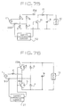
- Fig. 1 is a circuit diagram of a choke-input type of dc power-supply unit in the prior art disclosed in, for example, "Electric Cooperative Research Paper” Vol.46, No.2, p.78 (published by Society of Electric Cooperative Research).
- Fig. 1 is a circuit diagram of a choke-input type of dc power-supply unit in the prior art disclosed in, for example, "Electric Cooperative Research Paper” Vol.46, No.2, p.78 (published by Society of Electric Cooperative Research).
- reference numeral 1 means an ac power supply
- 2 means a reactor (inductive element) serially connected to the ac power supply
- 3 is a rectifier circuit (rectifying means) including diode bridges (rectifying devices) 4 to 7 connected to the ac power supply 1 and the reactor
- 8 is a smoothing circuit (smoothing means) including a capacitor 9 connected in parallel with the rectifier circuit
- 10 is the load connected to the smoothing circuit 8
- 11 is a dc power-supply unit including the reactor 2, the rectifier circuit 3, and the smoothing circuit 8.
- the diode bridges 4 and 7 of the rectifier circuit 3 are set in nonconducting state. As in the case of the half period, the diode bridges 5 and 6 of the rectifier circuit 3 cause the same charging current to flow in the capacitor 9 of the smoothing circuit 8 through the reactor 2 for the next half period.
- the source voltage e of the ac power supply 1 and current input into the dc power-supply unit 11 exhibit waveforms as shown in Figs. 2(a), (b). At this time, the voltage charged in the capacitor 9 is applied to the load 10.
- Fig. 3 is a circuit diagram of a conventional dc power-supply unit having an enhanced power factor, disclosed in, for example, Japanese Patent Application Laid-Open No. 2-299470.
- Fig. 3 descriptions of component parts identical with those of the choke-input type of dc power-supply unit in the prior art are omitted.
- reference numeral 12 means a transistor serving as switching means for short-circuiting the ac power supply 1 through the reactor 2, and 13 means a diode to prevent counter-current from the capacitor 9 of the smoothing circuit 8.
- the current path in a cutoff (OFF) state of the transistor 12 is established to pass through the ac power supply 1, the reactor 2, the diode bridge 4, the diode 13, the capacitor 9, and the diode bridge 7, and return to the ac power supply 1.
- the current path in the cutoff (OFF) state of the transistor 12 is established to pass through the ac power supply 1, the diode bridge 6, the diode 13, the capacitor 9, the diode bridge 5, and the reactor 2, and return to the ac power supply 1.
- the switching operation of the transistor 12 is repeated for each positive or negative half-wave of the voltage of the ac power-supply 1.
- the ac input current l s2 can serve as the input current with the reactor 2 as the load during the transistor 12 is ON, and increases for a time period when the transistor 12 is ON. Further, accumulated energy in the reactor 2 is discharged concurrently with the OFF state of the transistor 12, resulting in a damped conducting condition. Therefore, it is possible to combine ac input current l s1 (shown in Fig. 2(b)) with the input current l s2 of the conventional choke-input type of dc power-supply unit into combined ac input current l s3 as shown in Fig. 4.
- the ac input current l s3 is applied over an entire period including time periods T1, T2, and T3 as shown in Fig. 4. Consequently, a power factor between the ac input current l s3 and the source voltage V s can be improved greater than that between the source voltage V s and the input current l s1 of the conventional choke-input type of dc power-supply unit.
- Fig. 6 is a circuit diagram in which the reactor 2 of Fig. 1 is connected to the dc side of the rectifier circuit 3. Since an operation of each component part in this circuit diagram is substantially identical with that in case of Fig. 1, it is possible to provide its operating waveform diagram as shown in Fig. 5.
- the conventional choke-input type of dc power-supply unit is constructed as set forth above. Accordingly, residual voltage serving as dc voltage is left in the capacitor 9 of the smoothing circuit 8 so that the charging current can flow only during the source voltage exceeds the residual voltage, that is, only during the source voltage is in a vicinity of its peak.
- a large higher harmonic component in particular, the higher harmonic component of odd-numbered order such as third order, fifth order, seventh order, or eleventh order
- the power factor is reduced.
- the conventional dc power-supply unit having the enhanced power factor is constructed as set forth above. Therefore, it is possible to improve the power factor in the dc power-supply unit greater than that in the choke-input type of dc power-supply unit.
- the dc power-supply unit is not particularly useful for the best effect of power factor improvement since the transistor 12 is conducting for a constant period exclusively (i.e., immediately after the source voltage passes through the zero point).
- the energy accumulated in the reactor 2 excessively increases during the transistor 12 is conducting so that no input current can not flow for the period T3 when magnitude of the load is varied.
- Document EP-A-0 486 875 A2 discloses a dc power supply-unit comprising: rectifying means for converting ac power output from an ac power supply into dc power so as to feed to a load; an inductive element whose one end is connected to one terminal on the dc side of said rectifying means; switching means connected between the other end of said inductive element and the other terminal on the dc side of said rectifying means to perform a switching operation; and smoothing means connected in parallel with said switching means.
- transistors Ta and Tb are controlled on and off in such a manner that they are alternately switched on
- the control circuit serves to reduce the on-state period of the transistor Ta or Tb for reducing the switching loss.
- two transistors are alternately switched on to give the ac load current a sinusoidal waveform.
- the on period of the transistor Ta or Tb is not a predetermined period but depends on the area where the voltage output from the rectifying section is high.
- a dc power-supply unit comprising rectifying means for converting ac power output from an ac power supply into dc power so as to feed to a load; an inductive element whose one end is connected to one terminal on the dc side of said rectifying means; switching means connected between the other end of said inductive element and the other terminal on the dc side of said rectifying means to perform a switching operation; and smoothing means connected in parallel with said switching means; characterized by switch controlling means for turning on said switching means once for a predetermined period, said predetermined period occurring periodically every half period of said ac power output from said ac power supply, and having a constant length of up to said half period of said ac power output from said ac power supply, and being so determined as to provide a high power factor and/or a low current higher harmonic characteristic of said dc power-supply unit.
- charging current can flow according to the magnitude of the load even if the voltage of the ac power supply is lower than the capacitor voltage of the smoothing means.
- the power factor, the relative harmonic content, and/or the distortion in the waveform of the ac power may correspond to respective predetermined values.
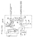
- Fig. 7 is a circuit diagram showing one embodiment of a dc power-supply unit according to the first aspect of the present invention.
- the same reference numerals are used for component parts identical with or equivalent to those of a dc power-supply unit in the prior art, and descriptions thereof are omitted.
- reference numeral 21 means a switch (switching means) connected between the other end of the reactor (inductive element) 2 and the other terminal on the dc side of the rectifier circuit (rectifying means) 3 to perform a switching operation
- 22 means a switch controlling circuit (switch controlling means) in which first and second delay times are set so as to, when ac voltage of the ac power supply 1 passes through a zero point, close the switch 21 after the first delay time T d from the passing through time, and open the switch 21 after the second delay time from the passing through time.
- reference numeral 23 means an ON timing generating circuit to generate an ON signal after the first delay time T d from the time when the ac voltage of the ac power supply 1 passes through the zero point
- 24 means an OFF timing generating circuit to generate an OFF signal after the second delay time from the time when the ac voltage of the ac power supply 1 passes through the zero point
- 25 is a switch driving circuit to drive the switch 21 in response to output signals from the ON timing generating circuit 23 and the OFF timing generating circuit
- 26 is a dc power-supply unit.
- the switch 21 is opened so that the short-circuit current which has been flowing in the reactor 2 passes through the diode 13 to become charging current in the capacitor 9 of the smoothing circuit (smoothing means) 8, and starts to decrease.
- the diode bridges 4, 7 or the diode bridges 5, 6) cause the charging current in the capacitor 9 to flow through the reactor 2 and the diode 13 as in the case of the conventional dc power-supply unit as described before.
- FIG. 8 Each operating waveform in each part at this time is shown in Fig. 8.
- Fig. 8 shows a source voltage waveform of the ac power supply 1
- (b) shows the output signal from the ON timing generating circuit 23
- (c) shows the output signal from the OFF timing generating circuit 24
- (d) shows an output signal from the switch driving circuit 25
- (e) shows input current of the dc power-supply unit 26.
- Fig. 9 is a diagram showing relations between the OFF signal output timing of the OFF timing generating circuit 24, and a power factor and a higher harmonic component of the input current of the dc power-supply unit 26 in case the ON signal for the switch 21 is generated from the ON timing generating circuit 23 at a certain time point in synchronization with the source voltage of the ac power supply 1 (for example, after a time T d from a zero crossing point of the source voltage) under a constant load.
- the transverse axis represents a ratio of the OFF signal output timing t off to a power supply period T 0 on the basis of the zero crossing point of the source voltage.
- the ON timing generating circuit 23 and the OFF timing generating circuit 24 are preset to output the optimal timing in synchronization with the source voltage of the ac power supply 1, respectively.
- the OFF signal output timing may be determined in the vicinity of the maximum power factor point with respect to the set ON signal output timing in case a particular weight is given to the power factor. Further, it must be noted that the OFF signal output timing may be determined so as to minimize the higher harmonic component of any desired specific order with respect to the set ON signal output timing in case the higher harmonic component of a specific order in the input current should be particularly reduced.
- the ON signal for the switch 21 output from the ON timing generating circuit 23 may be set depending upon a power factor characteristic shown in Fig. 10 under a constant load.
- the ordinate axis represents a delay time T d from the zero crossing point of the source voltage
- the transverse axis represents a conducting time T on of the switch 21, that is, a time obtained by subtracting the delay time T d from the OFF signal output timing t off on the basis of the zero crossing point of the source voltage.
- Fig. 10 is a contour map showing 0.8% or more power factor.
- the ON signal output timing may be set in the range.
- the ON timing generating circuit 23 and the OFF timing generating circuit 24 may be constructed as shown in Fig. 11 in case the ON signal output timing for the switch 21 is delayed by a time T d from the zero crossing point of the source voltage of the ac power supply 1, and the OFF signal output timing is delayed a given period from the zero crossing point.
- T d the ON signal output timing for the switch 21 is delayed by a time T d from the zero crossing point of the source voltage of the ac power supply 1
- the OFF signal output timing is delayed a given period from the zero crossing point.
- reference numeral 27 means a photocoupler whose input is connected to the ac power supply 1, 28 and 29 are input-output bias resistors, 30 is a one-shot multivibrator circuit using an output from the photocoupler 27 as a trigger input, 31 and 32 are respectively a resistor and a capacitor to set an output pulse width of the one-shot multivibrator circuit 30, 33 is a trailing edge detecting circuit, and 34, 35 are respectively a resistor and a capacitor to set a pulse width of a trailing edge detecting signal.
- reference numeral 36 means a one-shot multivibrator circuit using the output from the photocoupler 27 as a trigger input
- 37 and 38 are respectively a resistor and a capacitor to set an output pulse width of the one-shot multivibrator circuit 36
- 39 is a trailing edge detecting circuit
- 40, 41 are respectively a resistor and a capacitor to set a pulse width of a trailing edge detecting signal.
- the output transistor of the photocoupler 27 is turned OFF so that a high level signal is output.
- the one-shot multivibrator circuit 36 uses the output as the trigger input, and outputs a signal (high level signal) having the pulse width set by the resistor 37 and the capacitor 38. In this case, if the pulse width is set to the optimal delay time T d from the zero crossing point of source voltage, an output signal from the trailing edge detecting circuit 39 obtained by an output signal from the one-shot multivibrator circuit 36 can serve as the output signal from the ON timing generating circuit 23.
- the one-shot multivibrator circuit 30 uses the output from the photocoupler 27 as the trigger input, and outputs a signal (a high level signal) having a pulse width set by the resistor 31 and the capacitor 32. In this case, if the pulse width is set to the optimal OFF timing, an output signal from the trailing edge detecting circuit 33 obtained by an output signal of the one-shot multivibrator circuit 30 can serve as the output signal from the OFF timing generating circuit 24.
- the signals in synchronization with the source voltage can be obtained by setting output from the ON timing generating circuit 23 and the OFF timing generating circuit 24 on the basis of the zero crossing point of the source voltage of the ac power supply 1.
- the present invention should not be limited to the above means for obtaining the synchronizing signal, and may include another means as shown in a circuit embodiment in Fig. 12.
- reference numerals 42 to 45 mean rectifying diodes
- 46 and 47 are voltage dividing resistors
- 48 and 52 are comparator circuits
- 49, 50, 53, and 54 are reference voltage setting resistors for the comparator circuits 48, 52, and 51, 55 are leading edge detecting circuits.
- Fig. 13 is a diagram showing the operation of the circuit shown in Fig. 12.
- Fig. 13 shows a source voltage waveform of the ac power supply 1
- b shows an output waveform of the voltage dividing resistors 46 -and 47
- c shows an output waveform of the voltage dividing resistors 46 -and 47
- c shows an output waveform of the voltage dividing resistors 46 -and 47
- c shows an output waveform of the voltage dividing resistors 46 -and 47
- (c) and (e) show.output waveforms from the respective comparator-circuits 48 and 52
- d show output waveforms from the respective leading edge detecting circuits 51, 55.
- reference voltage of the comparator circuits 51, 55 are respectively set to the ON timing and the OFF timing for the switch 21, output from the leading edge detecting circuits 51, 55 can serve as output from the ON timing generating circuit 23 and the OFF timing geperating circuit 24, respectively.
- both of a reactor 2 and a switch 21 are arranged on the dc side of a subsequent stage of a rectifier circuit 3.
- the present invention should not be limited to the arrangement of the reactor 2 and the switch 21, and the reactor 2 may be disposed on the ac side as shown in Fig. 14 (according to the twenty-fourth aspect). In this case, the reactor 2 can be made smaller than would be in case the reactor 2 is disposed on the dc side.
- both of a reactor 2 and a switch 21 may be arranged on the ac side as shown in Fig. 15.
- both the reactor 2 and the switch 21 are arranged on the ac side as shown in Fig. 15, it is possible to omit the diode 13 of the capacitor 9 of the smoothing circuit 8 shown in Fig. 7 according to the embodiment 1 since the diode bridges 4 to 7 of the rectifier circuit 3 also serve as the diode 13.
- the plurality of reactors 2 may be provided to serve as an inductive element shown in Figs. 7, 14, and 15.
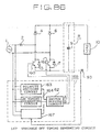
- the switch controlling circuit 22 of Fig. 7 may be constructed as shown in Fig. 17.
- reference numeral 58 means a zero point detecting circuit to detect a zero point of input current
- 59 and 60 are delay circuits to respectively output a signal after a first delay time and a second delay time when the zero point is detected by the zero point detecting circuit 58
- 61 is a transistor ON/OFF circuit to continuously output an ON signal and an OFF signal for a predetermined period when signals are output from the delay circuits 59, 60
- 62 is a switch driving circuit to drive the switch 21 in response to the output signal from the transistor ON/OFF circuit 61.
- Fig. 18 is a circuit diagram showing one embodiment according to the second aspect of the present invention.
- reference numeral 72 means an ON period setting circuit to set an ON period of the switch 21 by using the output signal from an ON timing generating circuit 23 as a trigger
- 73 means a switch driving circuit to drive a switch 21 according to an output signal from the ON period setting circuit 72
- And 71 is a switch controlling circuit (switch controlling means) including the ON timing generating circuit 23, the ON period setting circuit 72, and the switch driving circuit 73
- 74 is a dc power-supply unit.
- the ON timing generating circuit 23 When the ON timing generating circuit 23 outputs the ON signal in synchronization with the source voltage of the ac power supply 1 and according to time which is delayed by a preset time T d immediately after the source voltage passes through the zero point, the ON period setting circuit 72 outputs a signal output to close the switch 21 only for a preset period to the switch 21 through the switch driving circuit 73.
- the switch 21 is closed, as in the case of the embodiment 1 described before, the ac power supply 1 is short-circuited through the reactor 2 and the diode bridges 4 and 7 (or the diode bridges 5, 6) to conduct current, and the current gradually increases.
- the short-circuit current which has been flowing in the reactor 2 passes through the diode 13 to become charging current in the capacitor 9 of the smoothing circuit 8, and starts to decrease.
- the diode bridges 4, 7 or the diode bridges 5, 6) cause the charging current in the capacitor 9 to flow through the reactor 2 and the diode 13.
- a source voltage waveform of the ac power supply 1 and an input current waveform of the dc power-supply unit 74 are identical with those shown in Fig. 8 according to the embodiment 1.
- Fig. 19 is a diagram showing relations between a signal output period of the ON period setting circuit 72, and a power factor and a higher harmonic component of the input current of the dc power-supply unit 74 in case the ON signal for the switch 21 is generated from the ON timing generating circuit 23 at a certain time point in synchronization with the source voltage of the ac power supply 1 (for example, after a time T d from the zero crossing point of the source voltage) under a constant load.
- the transverse axis represents a ratio of an ON signal output period t on to the power supply period T 0 .
- the ON timing generating circuit 23 and the ON period setting circuit 72 are preset to output the optimal timing and the optimal ON period, respectively. Further, as in the embodiment 1, it must be noted that the ON timing and the ON period may be set depending upon, for example, an operating point to maximize the power factor, or another operating point to minimize a specific higher harmonic current of the input current.
- the ON timing generating circuit 23 and the ON period setting circuit 72 may be constructed as shown in Fig. 20 in case the ON signal output timing for the switch 21 is delayed by a delay time T d from the zero crossing point of the source voltage of the ac power supply 1.
- reference numeral 75 means a one-shot multivibrator circuit using the output from the photocoupler 27 as a trigger input
- 76, 77 are respectively a resistor and a capacitor to set an output pulse width of the one-shot multivibrator circuit 75, that is, the ON timing for the switch 21.
- reference numeral 78 means a one-shot multivibrator circuit using the output from the ON timing generating circuit 23 as the trigger input
- 79, 80 are respectively a resistor and a capacitor to set an output pulse width of the one-shot multivibrator circuit 78, that is, the ON period of the switch 21.
- the present invention should not be limited to the means on the basis of the zero crossing point of the source voltage as means for obtaining the signal in synchronization with the source voltage of the ac power supply 1.
- the present invention should not be limited to the arrangement of the reactor 2 and the switch 21 shown in Fig. 18.
- the reactor 2 may be disposed on the ac side as shown in Fig. 14, and both of the reactor 2 and the switch 21 may be arranged on the ac side as shown in Fig. 15.
- a voltage doubler rectifier circuit may be formed as shown in Fig. 16.
- the plurality of reactors 2 may be provided to serve as an inductive element.
- a switch controlling circuit 71 of Fig. 18 may be constructed as shown in Fig. 21.
- FIG. 22 An illustrative circuit is shown in Fig. 22.
- reference numeral 81 means a zero point detecting circuit to output a signal A when the input current is equal to or more than b, and is equal to or less than a.
- the zero point detecting circuit 81 has thresholds a, b with respect to the input current, and outputs "Lo" signal, that is, the signal A when the input current is equal to or more than b and is equal to or less than a. It is possible to provide signals B and C in the same process as that in the embodiment 1. Thereby, it is possible to perform the same operation as that in the embodiment 1, resulting in the same effect.
- Fig. 24 is a circuit diagram showing one embodiment according to the third aspect of the present invention.
- reference numeral 82 means a current sensor (short-circuit current detecting means) to detect short-circuit current which flows in the reactor 2 when a switch 21 is closed
- 83 means a short-circuit current detecting circuit to output an OFF signal for the switch 21 when an output from the current sensor 82 reaches a preset value
- 84 is a switch controlling circuit (switch controlling means) including the ON timing generating circuit 23, the short-circuit current detecting circuit 83, and the switch driving circuit 25, and 85 is a dc power-supply unit.
- the ON timing generating circuit 23 outputs the ON signal through the switch driving circuit 25 in synchronization with source voltage of an ac power supply 1 and according to timing which is delayed by a preset time T d immediately after the source voltage passes through the zero point. Subsequently, the switch 21 is closed so that the ac power supply 1 is short-circuited through a reactor 2 and diode bridges 4 and 7 (or diode bridges 5, 6) to conduct current, and the current gradually increases. When the short-circuit current increases and reaches the preset value, the short-circuit current detecting circuit 83 outputs the OFF signal for the switch 21 through the switch driving circuit 25 to open the switch 21.
- the short-circuit current which has been flowing in the reactor 2 passes through the diode 13 to become charging current in the capacitor 9 of the smoothing circuit 8, and starts to decrease. Thereafter, when the source voltage of the ac power supply 1 is in the vicinity of peak voltage, the diode bridges 4, 7 (or the diode bridges 5, 6) cause the charging current in the capacitor 9 to flow through the reactor 2 and the diode 13.
- a source voltage waveform of the ac power supply 1 and an input current waveform of the dc power-supply unit 85 are identical with those shown in Fig. 8 according to the embodiment 1.
- Fig. 25 is a diagram showing relations between a short-circuit current level to generate the OFF signal for the switch 21, and a power factor and a higher harmonic component of the input current of the dc power-supply unit 85 in case the ON signal for the switch 21 is generated from the ON timing generating circuit 23 at a certain time point in synchronization with the source voltage of the ac power supply 1 (for example, after a time T d from the zero crossing point of the source voltage) under a constant load.
- the transverse axis represents ratio of the short-circuit current level i P to generate the OFF signal for the switch 21 to average output current I AVG when the maximum load is applied to the dc power-supply unit 85.
- the ON timing generating circuit 23 and the short-circuit current detecting circuit 83 are preset to output the optimal timing and the optimal short-circuit current level, respectively. Further, as in the embodiment 1, it must be noted that the ON timing and the short-circuit current level may be set depending upon, for example, an operating point to maximize the power factor, or another operating point to minimize a specific higher harmonic current of the input current.
- the ON timing generating circuit 23 and the short-circuit current detecting circuit 83 may be constructed as shown in Fig. 26 in case ON signal output timing for the switch 21 is delayed by a delay time T d from the zero crossing point of the source voltage of the ac power supply 1.
- T d delay time
- reference numeral 86 means a comparator circuit
- 87 and 88 mean setting resistors to set the short-circuit current level to generate reference voltage of the comparator circuit 86, that is, the OFF signal for the switch 21
- 89 is a one-shot multivibrator circuit using an output signal from the comparator circuit 86 as a trigger
- 90, 91 are respectively a resistor and a capacitor to set an output pulse width of the one-shot multivibrator circuit 89, that is, a width of a pulse signal serving as OFF timing for the switch 21.
- the present invention should not be limited to the means on the basis of the zero crossing point of the source voltage as means for obtaining the signal in synchronization with the source voltage of the ac power supply 1.
- the present invention should not be limited to the arrangement of the reactor 2 and the switch 21 shown in Fig. 24.
- the reactor 2 may be disposed on the ac side as shown in Fig. 14, and both of the reactor 2 and the switch 21 may be arranged on the ac side as shown in Fig. 15.
- a voltage doubler rectifier circuit may be formed as shown in Fig. 16.
- the plurality of reactors 2 may be provided to serve as an inductive element.
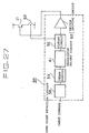
- the switch controlling circuit 84 of Fig. 24 may be constructed as shown in Fig. 27.
- reference numeral 92 means a cutoff circuit to cut off a driving signal for a switch 21.
- Fig. 28 is an operating waveform diagram showing the operation in Fig. 27.
- Fig. 29 is a circuit diagram showing one embodiment according to the fourth aspect of the present invention.
- reference numeral 93 means a current sensor (load condition detecting means) to detect load current
- 94 means a variable ON timing generating.circuit to generate an ON signal for a switch 21 in synch ronization with the source voltage, and according to timing according to a load condition detected by the current sensor 93
- 95 is a switch controlling circuit (switch controlling means) including the variable ON timing generating circuit 94, an OFF timing generating circuit 24, and a switch driving circuit 25, and 96 is a dc power-supply unit.
- variable ON timing generating circuit 94 outputs an ON signal through the switch driving circuit 25 in synchronization with the source voltage of an ac power supply 1, and according to the load condition detected by the current sensor 93. Consequently, the switch 21 is closed so that the ac power supply 1 is short-circuited through a reactor 2 and diode bridges 4 and 7 (or diode bridges 5, 6) to conduct current, and the current gradually increases. Subsequently, the OFF timing generating circuit 24 outputs the OFF signal through the switch driving circuit 25 in synchronization with the source voltage, resulting in opening the switch 21.
- the shorts-circuit current which has been flowing in the reactor 2 passes through a diode 13 to become charging current in a capacitor 9 of a smoothing circuit 8, and starts to decrease. Thereafter, when the source voltage of the ac power supply 1 is in the vicinity of peak voltage, the diode bridges 4, 7 (or the diode bridges 5, 6) cause the charging current in the capacitor 9 to flow through the reactor 2 and the diode 13.
- a source voltage waveform of the ac power supply 1 and the input current waveforms of the dc power-supply unit 96 under a light load and a heavy load as shown in Fig. 30.
- the operation is controlled so as to have a later ON signal output timing of the variable ON timing generating circuit 94 under a light load than the ON signal output timing under a heavy load.
- Fig. 31 is a diagram showing a relation between a load, and the ON signal output timing serving as the overall optimal operating point in view of a power factor and a current higher harmonic characteristic in case the OFF signal for the switch 21 is generated from the OFF timing generating circuit 24 at a certain time point in synchronization with the source voltage of the ac power supply 1 (for example, after a time point delayed by one-tenth of power supply period from a zero crossing point of the source voltage).
- the transverse axis represents a load normalized by rated load P 0
- the ordinate axis represents the ON signal output timing normalized by the power supply period T 0 .
- the output timing of the variable ON timing generating circuit 94 can be controlled according to the load condition based upon the relation shown in Fig. 31. Further, it must be noted that the output timing of the variable ON timing generating circuit 94 may be controlled according to the purpose. That is, while a particular weight is given to the power factor, the output timing may be controlled according to the load condition. Alternatively, while the particular weight is given to the current higher harmonic characteristic, the output timing may be controlled according to the load condition.
- the present invention should not be limited to this means as load condition detecting means.
- the present invention should not be limited to the means on the basis of the zero crossing point of the source voltage as means for obtaining the signal in synchronization with the source voltage of the ac power supply 1.
- the present invention should not be limited to the arrangement of the reactor 2 and the switch 21 shown in Fig. 29.
- the reactor 2 may be disposed on the ac side as shown in Fig. 14, and both of the reactor 2 and the switch 21 may be arranged on the ac side as shown in Fig. 15.
- a voltage doubler rectifier circuit may be formed as shown in Fig. 16.
- the plurality of reactors 2 may be provided to serve as an inductive element.
- Fig. 32 is a circuit diagram showing one embodiment according to the fifth aspect of the present invention.
- reference numeral 97 means a switch controlling circuit (switch controlling means) including a variable ON timing generating circuit 94, an ON period setting circuit 72, and a switch driving circuit 73, and 98 is a dc power-supply unit.
- variable ON timing generating circuit 94 outputs an ON signal in synchronization with the source voltage of the ac power supply 1, and according to a load condition detected by the current sensor 93. Consequently, the ON period setting circuit 72 outputs a signal output to close a switch 21 only for a preset period through the switch driving circuit 73 to the switch 21.
- the switch 21 is closed, as in the embodiment 11 described before, the ac power supply 1 is short-circuited through a reactor 2 and diode bridges 4, and 7 (or diode bridges 5, 6) to conduct current, and the current gradually increases.
- a source voltage waveform of the ac power supply 1, and input current waveforms of the dc power-supply unit 98 under a light load and a heavy load as shown in Fig. 33.
- the operation is controlled so as to have an earlier ON signal output timing of the variable ON timing generating circuit 96 under a light load than the ON signal output timing under a heavy load.
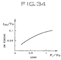
- Fig. 34 is a diagram showing a relation between a load, and the ON signal output timing serving as the overall optimal operating point in view of the power factor and a current higher harmonic characteristic in case an ON signal output period of the ON period setting circuit 72 is set to a certain period (for example, one-twentieth of source voltage period).
- the transverse axis represents a load normalized by rated load P 0
- the ordinate axis represents the ON signal output timing normalized by the power supply period T 0 .
- the output timing of the variable ON timing generating circuit 94 can be controlled according to the load condition based upon the relation shown in Fig. 34.
- the output timing of the variable ON timing generating circuit 94 may be controlled according to the purpose. That is, while a particular weight is given to the power factor, the output timing may be controlled according to the load condition. Alternatively, while the particular weight is given to the current higher harmonic characteristic, the output timing may be controlled according to the load condition.
- the present invention should not be limited to the load current detecting means as means for detecting the magnitude of the load condition.
- the load current detecting means as means for detecting the magnitude of the load condition.
- the present invention should not be limited to the means on the basis of the zero crossing point of the source voltage as means for obtaining the signal in synchronization with the source voltage of the ac power supply 1.
- the present invention should not be limited to the arrangement of the reactor 2 and the switch 21 shown in Fig. 32.
- the reactor 2 may be disposed on the ac side as shown in Fig. 14, and both of the reactor 2 and the switch 21 may be arranged on the ac side as shown in Fig. 15.
- a voltage doubler rectifier circuit may be formed as shown in Fig. 16.
- the plurality of reactors 2 may be provided to serve-as an inductive element.
- reference numeral 99 means a load detecting circuit to decide magnitude of load according to a signal from a current sensor 200
- 100 means a switching start time setting timer to set a switching start time under a heavy load in synchronization with source voltage
- 101 is an ON period setting timer to set an ON time under the heavy load
- 102 is a switching start time setting timer to set the switching start time sunder a light load in synchronization with the source voltage
- 103 is an ON period setting timer to set the ON time under the light load
- 104 is a timing switching circuit by which the timing is switched over to either timing for heavy load or timing for light load in response to a signal from the load detecting circuit 99
- 105 is a switch keying circuit to open and close a switch 21 according to the ON/OFF timing output from the timing switching circuit 104.
- the switching start time setting timers 100 and 102 output the ON signals in synchronization with the source voltage of the ac power supply 1 to actuate the ON period setting timers 101 and 103 so as to output the ON signals to the timing switching circuit 104.
- the magnitude of the load is decided in the load detecting circuit 99 depending upon the signal from the current sensor 200 to output the result to the timing switching circuit 104.
- the timing switching circuit 104 is switched over so as to output the signal from the ON period setting timer 101 to the switch keying circuit 105 if the signal from the load detecting circuit 99 is a heavy load signal, and output the signal from the ON period setting timer 103 to the switch keying circuit 105 if it is a light load signal.
- the switch keying circuit 105 receives the ON signal from the timing switching circuit 104 to close the switch 21.
- the ac power supply 1 When the switch 21 is closed, the ac power supply 1 is short-circuited through a reactor 2 and diode bridges 4 and 7 (or diode bridges 5, 6) to conduct current, and the current gradually increases. Subsequently, the ON period setting timers 101 and 103 output the OFF signals to the timing switching circuit 104.
- the magnitude of the load is decided in the load detecting circuit 99 depending upon the signal from the current sensor 200 to output the result to the timing switching circuit 104.
- the timing switching circuit 104 is switched over so as to output the signal from the ON period setting timer 101 to the switch keying circuit 105 if the signal from the load detecting circuit 99 is a heavy load signal, and output the signal from the ON period setting timer 103 to the switch keying circuit 105 if it is a light load signal.
- the switch keying circuit 105 receives the OFF signal from the timing switching circuit 104 to open the switch 21.
- the switch 21 When the switch 21 is opened, the short-circuit current which has been flowing in the reactor 2 passes through the diode 13 to become charging current in the capacitor 9, and starts to decrease. Thereafter, when the source voltage of the ac power supply 1 is in the vicinity of peak voltage, the diode bridges 4, 7 (or the diode bridges 5, 6) cause the charging current in the capacitor 9 to flow through the reactor 2 and the diode 13.
- Fig. 36 shows a source voltage waveform
- b shows a zero cross detecting signal
- c shows a switching start time output signal
- d shows the ON time
- e shows a current waveform.
- Fig. 37 is a circuit diagram showing one embodiment according to the sixth aspect of the present invention.
- reference numeral 106 means a switch controlling circuit (switch controlling means) including a variable ON timing generating circuit 94, a short-circuit current detecting circuit 83, and a switch driving circuit 25, and 107 is a dc power-supply unit.
- variable ON timing generating circuit 94 outputs an ON signal through the switch driving circuit 25 in synchronization with the source voltage of the ac power supply 1, and according to the load condition detected by the current sensor 93. Subsequently, the switch 21 is closed so that the ac power supply 1 is short-circuited through a reactor 2 and diode bridges 4 and 7 (or diode bridges 5, 6) to conduct current, and the current gradually increases.
- the short-circuit current detecting circuit 83 outputs an OFF signal for the switch 21 through the switch driving circuit 25 to open the switch 21.
- the short-circuit current which has been flowing in the reactor 2 passes through a diode 13 to become charging current in a capacitor 9 of a smoothing circuit 8, and starts to decrease. Thereafter, when the source voltage of the ac power supply 1 is in the vicinity of peak voltage, the diode bridges 4, 7 (or the diode bridges 5, 6) cause the charging current in the capacitor 9 to flow through the reactor 2 and the diode 13.
- a source voltage waveform of the ac power supply 1, and input current waveforms of the dc power-supply unit 107 under a light load and a heavy load as shown in Fig. 38.
- the operation is controlled so as to have a later ON signal output timing of the variable ON timing generating circuit 94 under a light load than the ON signal output timing under a heavy load.
- Fig. 39 is a diagram showing a relation between a load, and the ON signal output timing serving as the overall optimal operating point in view of a power factor and a current higher harmonic characteristic in case a short-circuit level to generate the OFF signal of the switch 21 is set to a predetermined value (for example, four-fifths of average current under the maximum load).
- the transverse axis represents a load normalized by rated load P 0
- the ordinate axis represents the ON signal output timing normalized by the power supply period T 0 .
- the output timing of the variable ON timing generating circuit 94 can be controlled according to the load condition based upon the relation shown in Fig. 39.
- the output timing of the variable ON timing generating circuit 94 may be controlled according to the purpose. That is, while a particular weight is given to the power factor, the output timing may be controlled according to the load condition. Alternatively, while the particular weight is given to the current higher harmonic characteristic, the output timing may be controlled according to the load condition.
- the present invention should not be limited to the load current detecting means as means for detecting the magnitude of the load condition.
- the load current detecting means as means for detecting the magnitude of the load condition.
- the present invention should not be limited to the means on the basis of the zero crossing point of the source voltage as means for obtaining the signal in synchronization with the source voltage of the ac power supply 1.
- the present invention should not be limited to the arrangement of the reactor 2 and the switch 21 shown in Fig. 37.
- the reactor 2 may be disposed on the ac side as shown in Fig. 14, and both of the reactor 2 and the switch 21 may be arranged on the ac side as shown in Fig. 15.
- a voltage doubler rectifier circuit may be formed as shown in Fig. 16.
- the plurality of reactors 2 may be provided to serve as an inductive element.
- circuit shown in Fig. 37 according to the embodiment 14 may be constructed as shown in Fig. 40.
- reference numeral 108 means an overcurrent detecting circuit to decide overcurrent depending upon a signal from a current sensor 82.
- Switching start time setting timers 100 and 102 output ON signals in synchronization with source voltage of an ac power supply 1 to actuate ON period setting timers 101 and 103 so as to output the ON signals to a timing switching circuit 104.
- the magnitude of the load is decided in a load detecting circuit 99 depending upon a signal from a current sensor 200 to output the result to the timing switching circuit 104.
- the timing switching circuit 104 is switched over so as to output the signal from the ON period setting timer 101 to a switch keying circuit 105 if the signal from the load detecting circuit 99 is a heavy load signal, and output the signal from the ON period setting timer 103 to the switch keying circuit 105 if it is a light load signal.
- the switch keying circuit 105 receives the ON signal from the timing switching circuit 104 to close the switch 21.
- the ac power supply 1 When the switch 21 is closed, the ac power supply 1 is short-circuited through a reactor 2 and diode bridges 4 and 7 (or diode bridges 5, 6) to conduct current, and the current gradually increases. Subsequently, the ON period setting timers 101 and 103 output an OFF signals to the timing switching circuit 104.
- the magnitude of the load is decided in the load detecting circuit 99 depending upon the signal from the current sensor 200 to output the result to the timing switching circuit 104.
- the timing switching circuit 104 is switched over so as to output the signal from the ON period setting timer 101 to the switch keying circuit 105 if the signal from the load detecting circuit 99 is a heavy load signal, and output the signal from the ON period setting timer 103 to the switch keying circuit 105 if it is a light load signal.
- the switch keying circuit 105 receives the OFF signal from the timing switching circuit 104 to open the switch 21.
- the switch 21 When the switch 21 is opened, the short-circuit current which has been flowing in the reactor 2 passes through a diode 13 to become charging current in a capacitor 9, and starts to decrease. Thereafter, when the source voltage of the ac power supply 1 is in the vicinity of peak voltage, the diode bridges 4, 7 (or the diode bridges 5, 6) cause the charging current in the capacitor 9 to flow through the reactor 2 and the diode 13.
- the overcurrent detecting circuit 108 detects that the signal from the current sensor 82 is the overcurrent in a condition where the switch 21 is closed, the overcurrent detecting circuit 108 outputs a reset signal to the switching start time setting timers 100 and 102, and to the ON period setting timers 101 and 103. Consequently, the ON period is terminated so that the ON period setting timers 101 and 103 output the OFF signals through the timing switching circuit 104 to the switch keying circuit 105, resulting in opening the switch 21.
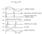
- Fig. 41 shows a source voltage waveform
- b shows a zero cross detecting signal
- c shows a switching start time output signal
- d shows the overcurrent
- e shows a switching OFF signal
- f shows the ON time
- g shows a current waveform of the power supply.
- Fig. 42 is a circuit diagram showing one embodiment according to the seventh aspect of the present invention.
- reference numeral 109 means a variable OFF timing generating circuit to generate an OFF signal for a switch 21 according to timing in synchronization with source voltage, and according to a load condition detected by a current sensor 93
- 110 means a switch controlling circuit (switch controlling means) including a variable ON timing generating circuit 23, the variable OFF timing generating-circuit 109, and a switch driving circuit 25, and 111 is a dc power-supply unit.
- An ON timing generating circuit 23 outputs an ON signal through a switch driving circuit 25 in synchronization with the source voltage of an ac power supply 1. Accordingly, the switch 21 is closed so that the ac power supply 1 is short-circuited through a reactor 2 and diode bridges 4 and 7 (or diode bridges 5, 6) to conduct current, and the current gradually increases. Subsequently, the variable OFF timing generating circuit 109 outputs the OFF signal through the switch driving circuit 25 in synchronization with the source voltage, and according to a load condition detected by the current sensor 93, resulting in opening the switch 21.
- the short-circuit current which has been flowing in the reactor 2 passes through a diode 13 to become charging current in a capacitor 9 of a smoothing circuit 8, and starts to decrease. Thereafter, when the source voltage of the ac power supply 1 is in the vicinity of peak voltage, the diode bridges 4, 7 (or the diode bridges 5, 6) cause the charging current in the capacitor 9 to flow through the reactor 2 and the diode 13.
- a source voltage waveform of the ac power supply 1 and input current waveforms of the dc power-supply unit 111 under a light load and a heavy load as shown in Fig. 43.
- the operation is controlled so as to have an earlier OFF signal output timing of the variable OFF timing generating circuit 109 under a light load than the OFF signal output timing under a heavy load.
- Fig. 44 is a diagram showing a relation between a load, and the OFF signal output timing serving as the overall optimal operating point in view of a power factor and a current higher harmonic characteristic in case the ON timing generating circuit 23 generates the ON signal for the switch 21 at a certain time point (for example, a time point delayed by one-twentieth of power supply period from a zero crossing point of the source voltage).
- the transverse axis represents a load normalized by rated load P 0
- the ordinate axis represents the ON signal output timing normalized by the power supply period T 0 .
- the output timing of the variable OFF timing generating circuit 109 can be controlled according to the load condition based upon the relation shown in Fig. 44.
- the output timing of the variable OFF timing generating circuit 109 may be controlled according to the purpose. That is, while a particular weight is given to the power factor, the output timing may be controlled according to the load condition. Alternatively, while the particular weight is given to the current higher harmonic characteristic, the output timing may be controlled according to the load condition.
- the present invention should not be limited to the load current detecting means as means for detecting the magnitude of the load condition.
- the load current detecting means as means for detecting the magnitude of the load condition.
- the present invention should not be limited to the means on the basis of the zero crossing point of the source voltage as means for obtaining the signal in synchronization with the source voltage of the ac power supply 1.
- the present invention should not be limited to the arrangement of the reactor 2 and the switch 21 shown in Fig. 42.
- the reactor 2 may be disposed on the ac side as shown in Fig. 14, and both of the reactor 2 and the switch 21 may be arranged on the ac side as shown in Fig. 15.
- a voltage doubler rectifier circuit may be formed as shown in Fig. 16.
- the plurality of reactors 2 may be provided to serve as an inductive element.
- the switch controlling circuit 110 shown in Fig. 42 may be constructed as shown in Fig. 45.
- reference numeral 112 means a second delay circuit
- 113 means a second transistor ON/OFF circuit
- 114 is a load detector to convert the input current into electric energy consumed by a load
- 115 is a switching signal generator to output a switching signal in response to a signal from the load detecting detector 114
- 116 is a signal switch.
- the delay circuit 59 provides a signal B 1 which is delayed by a time t 11 from a signal A, and the transistor ON/OFF circuit 61 provides a signal C 1 to turn ON a switch 21 for a time interval t 21 .
- the second delay circuit 112 provides a signal B2 which is delayed by a time t 12 from the signal A, and the second transistor ON/OFF circuit 113 provides a signal C to turn ON the switch 21 for a time period t 22 .
- the load detector 114 outputs a signal P indicating the electric energy consumed by the load depending upon the input current.
- the switching signal generator 115 outputs a signal "Hi” in case the signal P exceeds a predetermined reference value Q.
- the signal switch 116 is switched over to receive the signal C 1 from the transistor ON/OFF circuit 61 when an output signal R from the switching signal generator 115 is "Lo,” or to receive the signal C 2 from the second transistor ON/OFF circuit 113 when the output signal R is "Hi.”
- third and fourth delay circuits and transistor ON/OFF circuits so as to perform a switching operation.
- the switch controlling circuit 110 shown in Fig. 42 may be constructed as shown in Fig. 47.
- reference numeral 141 means a frequency detector to detect frequency of a power supply depending upon input current.
- signals A, B 1 , B 2 , C 1 , and C 2 are provided by detecting a zero point of the input current in the same process as that in the embodiment 17.
- the frequency detector 141 detects whether power supply frequency is 50 Hz or 60 Hz, and outputs "Lo” if 50 Hz, or outputs "Hi” if 60 Hz.
- the signal switch 116 is switched over to receive the signal C 1 from a transistor ON/OFF circuit 61 if 50 Hz, and receive the signal C 2 from a second transistor ON/OFF circuit 113 if 60 Hz. Thereby, it is possible to provide the optimal power factor, and the optimal higher harmonic according to the frequency.
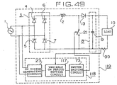
- Fig. 49 is a circuit diagram showing one embodiment according to the eighth aspect of the present invention.
- reference numeral 117 means a variable ON period setting circuit to use an output signal from an ON timing generating circuit 23 as a trigger so as to set the ON period of a switch 21 according to a load condition detected by a current sensor 93
- 118 means a switch controlling circuit (switch controlling means) including the ON timing generating circuit 23, the variable ON period setting circuit 117, and the switch driving circuit 73, and 119 is a dc power-supply unit.
- the ON timing generating circuit 23 outputs the ON signal in synchronization with the source voltage of the ac power supply 1. Consequently, the variable ON period setting circuit 117 outputs a signal output to close the switch 21 only for a preset period according to the load condition detected by the current sensor 93 through the switch driving circuit 73 to the switch 21.
- the switch 21 is closed, as in the embodiment 1 described before, the ac power supply 1 is short-circuited through a reactor 2 and diode bridges 4 and 7 (or diode bridges 5, 6) to conduct current, and the current gradually increases.
- the short-circuit current which has been flowing in the reactor 2 passes through a diode 13 to become charging current in a capacitor 9 of a smoothing circuit 8, and starts to decrease.
- the diode bridges 4, 7 or the diode bridges 5, 6) cause the charging current in the capacitor 9 to flow through the reactor 2 and the diode 13.
- a source voltage waveform of the ac power supply 1, and input current waveforms of the dc power-supply unit 119 under a light load and a heavy load as shown in Fig. 50.
- the operation is controlled so as to have a shorter ON signal output period of the variable ON period setting circuit 117 under a light load than the ON signal output period under a heavy load.
- Fig. 51 is a diagram showing a relation between a load, and the ON signal output timing serving as the overall optimal operating point in view of a power factor and a current higher harmonic characteristic in case the ON timing generating circuit 23 generates the ON signal for the switch 21 at a certain time point (for example, a time point which is delayed by one-twentieth of source voltage period from a zero crossing point of the source voltage).
- the transverse axis represents a load normalized by rated load P 0
- the ordinate axis represents the ON period normalized by the power supply period T 0 .
- an ON signal output interval of the variable ON period setting circuit 117 can be controlled according to the load condition based upon the relation shown in Fig. 51.
- the ON signal output interval of the variable ON period setting circuit 117 may be controlled according to the purpose. That is, while a particular weight is given to the power factor, the ON signal output interval may be controlled according to the load condition. Alternatively, while the particular weight is given to the current higher harmonic, the ON signal output interval may be controlled according to the load condition.
- the present invention should not be limited to the load current detecting means as means for detecting the magnitude of the load condition.
- the load current detecting means as means for detecting the magnitude of the load condition.
- the present invention should not be limited to the means on the basis of the zero crossing point of the source voltage as means for obtaining the signal in synchronization with the source voltage of the ac power supply 1.
- the present invention should not be limited to the arrangement of the reactor 2 and the switch 21 shown in Fig. 49.
- the reactor 2 may be disposed on the ac side as shown in Fig. 14, and both of the reactor 2 and the switch 21 may be arranged on the ac side as shown in Fig. 15.
- a voltage doubler rectifier circuit may be formed as shown in Fig. 16.
- the plurality of reactors 2 may be provided to serve as an inductive element.
- the switch controlling circuit 118 shown in Fig. 49 may be constructed as shown in Fig. 52.
- a delay circuit 59 to determine t 1 and a transistor ON/OFF circuit 61 to determine t 2 can linearly vary t 1 , t 2 in response to an analog signal which is externally fed.
- t 1 , t 2 are varied by a signal from the load detector 114.
- the signal P from the load detector 114 increases or decreases according to electric energy consumed in a load 10 so that t 1 , t 2 of a delay circuit 59 and the transistor ON/OFF circuit 61 increase or decrease. That is, when the signal P is varied from P1 to P2 as shown in Fig.
- t 1 , t 2 are similarly varied from t 11 to t 12 , and from t 21 to t 22 , Thereby, there are provided operating waveforms as shown in Fig. 53, and it is possible to provide the optimal power factor, and the optimal higher harmonic according to the electric energy consumed in the load 10.
- Fig. 54 is a circuit diagram showing one embodiment according to the ninth aspect of the present invention.
- reference numeral 120 means a variable short-circuit current detecting circuit to output an OFF signal for the switch 21 when an output from a current sensor 82 reaches a value which is set according to a load condition detected by a current sensor 93
- 121 means a switch controlling circuit (switch controlling means) including a ON timing generating circuit 23, the variable short-circuit current detecting circuit 120, and a switch driving circuit 25, and 122 is a dc power-supply unit.
- the ON timing generating circuit 23 outputs an ON timing signal through the switch driving circuit 25 in synchronization with the source voltage of an ac power supply 1. Consequently, the switch 21 is closed so that the ac power supply 1 is short-circuited through a reactor 2 and diode bridges 4 and 7 (or diode bridges 5, 6) to conduct current, and the current gradually increases.
- the short-circuit current increases and reaches the value which is set according to the load condition detected by the current sensor 93
- the variable short-circuit current detecting circuit 120 outputs the OFF signal for the switch 21 through the switch driving circuit 25 to open the switch 21.
- the short-circuit current which has been flowing in the reactor 2 passes through a diode 13 to become charging current in a capacitor 9 of a smoothing circuit 8, and starts to decrease. Thereafter, when the source voltage of the ac power supply 1 is in the vicinity of peak voltage, the diode bridges 4, 7 (or the diode bridges 5, 6) cause the charging current in the capacitor 9 to flow through the reactor 2 and the diode 13.
- a source voltage waveform of the ac power supply 1 and input current waveforms of the dc power-supply unit 122 under a light load and a heavy load as shown in Fig. 55.
- the operation is controlled so as to have a lower short-circuit current setting level of the variable short-circuit current.
- detecting circuit 102 under a light load than the short-circuit current setting level under a heavy load.
- Fig. 56 is a diagram showing a relation between a load, and a short-circuit current level serving as the overall optimal operating point in view of apower factor and a higher harmonic characteristic in case the ON timing generating circuit 23 generates the ON signal for the switch 21 at a certain time point in synchronization with the source voltage of the ac power supply 1 (for example, a time point which is delayed by one-twentieth of source voltage period from a zero crossing point of the source voltage).
- the transverse axis represents a load normalized by rated load P 0
- the ordinate axis represents the short-circuit current setting level normalized by average current I AVG under the maximum load.
- the short-circuit current setting level of the variable short-circuit current detecting circuit 120 can be controlled according to the load condition based upon the relation shown in Fig. 56. Further, it must be noted that the short-circuit current setting level of the variable short-circuit current detecting circuit 120 may be controlled according to the purpose. That is, while a particular weight is given to the powerfactor, the short-circuit current setting level may be controlled according to the load condition. Alternatively, while the particular weight is given to the current higher harmonic, the short-circuit current setting level may be controlled according to the load condition.
- the present invention should not be limited to the load current detecting means as means for detecting the magnitude of the load condition.
- the load current detecting means as means for detecting the magnitude of the load condition.
- the present invention should not be limited to the means on the basis of the zero crossing point of the source voltage as means for obtaining the signal in synchronization with the source voltage of the ac power supply 1.
- the present invention should not be limited to the arrangement of the reactor 2 and the switch 21 shown in Fig. 54.
- the reactor 2 may be disposed on the ac side as shown in Fig. 14, and both of the reactor 2 and the switch 21 may be arranged on the ac side as shown in Fig. 15.
- a voltage doubler rectifier circuit may be formed as shown in Fig. 16.
- the plurality of reactors 2 may be provided to serve as an inductive element.
- Fig. 57 is a circuit diagram showing one embodiment according to the tenth aspect of the present invention.
- reference numeral 123 means a switch controlling circuit (switch controlling means) including a variable ON timing generating circuit 94, a variable OFF timing generating circuit 109, and a switch driving circuit 25, and 124 means a dc power-supply unit.
- variable ON timing generating circuit 94 outputs an ON signal through the switch driving circuit 25 in synchronization with source voltage of an ac power supply 1, and according to a load condition detected by the current sensor 93. Consequently, the switch 21 is closed so that the ac power supply 1 is short-circuited through a reactor 2 and diode bridges 4 and 7 (or diode bridges 5, 6) to conduct current, and the current gradually increases. Subsequently, the variable OFF timing generating circuit 109 outputs a OFF signal through the switch driving circuit 25 in synchronization with the source voltage and according to the load condition detected by the current sensor 93, resulting in opening the switch 21.
- the short-circuit current which has been flowing in the reactor 2 passes through a diode 13 to become charging current in a capacitor 9 of a smoothing circuit 8, and starts to decrease. Thereafter, when the source voltage of the ac power supply 1 is in the vicinity of peak voltage, the diode bridges 4, 7 (or the diode bridges 5, 6) cause the charging current in the capacitor 9 to flow through the reactor 2 and the diode 13.
- each output timing of the variable ON timing generating circuit 94 and the variable OFF timing generating circuit 109 can be controlled according to the load condition so as to provide the overall optimal operating point in view of a power factor and a current higher harmonic characteristic.
- the output timing of the variable ON timing generating circuit 94 and the variable OFF timing generating circuit 109 may be controlled according to the purpose. That is, while a particular weight is given to the power factor, the output timing may be controlled according to the load condition. Alternatively, while the particular weight is given to the current higher harmonic characteristic, the output timing may be controlled according to the load condition.
- the present invention should not be limited to the load current detecting means as means for detecting the magnitude of the load condition.
- the load current detecting means as means for detecting the magnitude of the load condition.
- the present invention should not be limited to the means on the basis of the zero crossing point of the source voltage as means for obtaining the signal in synchronization with the source voltage of the ac power supply 1.
- the present invention should not be limited to the arrangement of the reactor 2 and the switch 21 shown in Fig. 57.
- the reactor 2 may be disposed on the ac side as shown in Fig. 14, and both of the reactor 2 and the switch 21 may be arranged on the ac side as shown in Fig. 15.
- a voltage doubler rectifier circuit may be formed as shown in Fig. 16.
- the plurality of reactors 2 may be provided to serve as an inductive element.
- Fig. 59 is a circuit diagram showing one embodiment according to the eleventh aspect of the present invention.
- reference numeral 125 means a switch controlling circuit (switch controlling means) including a variable ON timing generating circuit 94, a variable ON period setting circuit 117, and a switch driving circuit 73, and 126 means a dc power-supply unit.
- variable ON timing generating circuit 94 outputs a ON signal in synchronization with the source voltage of an ac power supply 1, and according to a load condition detected by the current sensor 93. Consequently, the variable ON period setting circuit 117 outputs a signal output to close a switch 21 only for a preset period which is set according to the load condition detected by the current sensor 93 through the switch driving circuit 73 to the switch 21.
- the switch 21 is closed, as in the embodiment 1 described before, the ac power supply 1 is short-circuited through a reactor 2 and diode bridges 4 and 7 (or diode bridges 5, 6) to conduct current, and the current gradually increases.
- the short-circuit current which has been flowing in the reactor 2 passes through the diode 13 to become charging current in a capacitor 9 of a smoothing circuit 8, and starts to decrease.
- the diode bridges 4, 7 or the diode bridges 5, 6) cause the charging current in the capacitor 9 to flow through the reactor 2 and the diode 13.
- each output timing of the variable ON timing generating circuit 94 and the variable ON period setting circuit 117 can be controlled according to the load condition so as to provide the overall optimal operating point in view of a power factor and a current higher harmonic characteristic.
- the output timing of the variable ON timing generating circuit 94 and the variable ON period setting circuit 117 may be controlled according to the purpose. That is, while a particular weight is given to the power factor, the output timing may be controlled according to the load condition. Alternatively, while the particular weight is given to the current higher harmonic, the output timing may be controlled according to the-load condition.
- the present invention should not be limited to the load current detecting means as means for detecting the magnitude of the load condition.
- the load current detecting means as means for detecting the magnitude of the load condition.
- the present invention should not be limited to the means on the basis of the zero crossing point of the source voltage as means for obtaining the signal in synchronization with the source voltage of the ac power supply 1.
- the present invention should not be limited to the arrangement of the reactor 2 and the switch 21 shown in Fig. 59.
- the reactor 2 may be disposed on the ac side as shown in Fig. 14, and both of the reactor 2 and the switch 21 may be arranged on the ac side as shown in Fig. 15.
- a voltage doubler rectifier circuit may be formed as shown in Fig. 16.
- the plurality of reactors 2 may be provided to serve as an inductive element.
- Fig. 60 is a circuit diagram showing one embodiment according to the twelfth aspect of the present invention.
- reference numeral 127 means a switch controlling circuit (switch controlling means) including a variable ON timing generating circuit 94, a variable short-circuit current detecting circuit 120, and a switch driving circuit 25, and 128 means a dc power-supply unit.
- variable ON timing generating circuit 94 outputs a ON signal through the switch driving circuit 25 in synchronization with the source voltage of an ac power supply 1, and according to a load condition detected by a current sensor 93. Consequently, the switch 21 is closed so that the ac power supply 1 is short-circuited through a reactor 2 and the diode bridges 4 and 7 (or the diode bridges 5, 6) to conduct current, and the current gradually increases.
- the variable short-circuit current detecting circuit 120 outputs a OFF signal for the switch 21 through the switch driving circuit 25 to open the switch 21.
- the short-circuit current which has been flowing in the reactor 2 passes through a diode 13 to become charging current in a capacitor 9 of a smoothing circuit 8, and starts to decrease. Thereafter, when the source voltage of the ac power supply 1 is in the vicinity of peak voltage, the diode bridges 4, 7 (or the diode bridges 5, 6) cause the charging current in the capacitor 9 to flow through the reactor 2 and the diode 13.
- each output timing of the: variable ON timing generating circuit 94 and a short-circuit current setting level of the variable short-circuit current detecting circuit 120 can be controlled according to the load condition so as to provide the overall optimal operating point in view of a power factor and a current higher harmonic characteristic. Further, it must be noted that the output timing of the variable ON timing generating circuit 94 and the short-circuit current setting level of the variable short-circuit current detecting circuit 120 may be controlled according to the purpose.
- the output timing and the short-circuit current setting level may be controlled according to the load condition.
- the particular weight is given to the current higher harmonic, the output timing and the short-circuit current setting level may be controlled according to the load condition.
- the present invention should not be limited to the load current detecting means as means for detecting the magnitude of the load condition.
- the load current detecting means as means for detecting the magnitude of the load condition.
- the present invention should not be limited to the means on the basis of the zero crossing point of the source voltage as means for obtaining the signal in synchronization with the source voltage of the ac power supply 1.
- the present invention should not be limited to the arrangement of the reactor 2 and the switch 21 shown in Fig. 60.
- the reactor 2 may be disposed on the ac side as shown in Fig. 14, and both of the reactor 2 and the switch 21 may be arranged on the ac side as shown in Fig. 15.
- a voltage doubler rectifier circuit may be formed as shown in Fig. 16.
- the plurality of reactors 2 may be provided to serve as an inductive element.
- the reactor 2 serving as the inductive element with a given inductance.
- the reactor 2 may be provided to have a plurality of variable inductance.
- the reactor 2 may be provided with tap terminals 127 and 128 so as to trigger a thyristor 129 such that the reactor 2 can have a greater inductance under a light load, and trigger a thyristor 130 such that the reactor 2 can have a less inductance under a heavy load, resulting in the variable inductance.
- a source voltage waveform of the ac power supply 1 and input current waveforms of the dc power-supply unit 131 under the light load and the heavy load as shown in, for example, Fig. 62.
- a delay time T d from a zero crossing point of the source voltage and a conducting time T on of the switch 21, or variation of an OFF timing t off even if the load fluctuates.
- Fig. 63 is a circuit diagram showing one embodiment according to the thirteenth and fourteenth aspects of the present invention.
- reference numeral 132 means a power factor detector (correcting means) to calculate a power factor depending upon input current and source voltage
- 133 means a computing element (correcting means) to correct a delay time set in a delay circuit 59 and an ON signal output time in a transistor ON/OFF circuit 61 by comparing the calculated power factor with a power factor command value which is externally fed.
- Fig. 64 in case a signal COS ⁇ from the power factor detector 132 becomes greater or less than the command value COS ⁇ *, an output from the computing element 133 is increased or decreased to vary values of t 1 and t 2 in order to correct the power factor of the source voltage so as to correspond to the command value. Thereby, it is possible to continuously provide the optimal power factor according to the power factor command value.
- Fig. 65 is a circuit diagram showing one embodiment according to the fifteenth and sixteenth aspects of the present invention.
- reference numeral 135 means a relative harmonic content detector (correcting means) to calculate a relative harmonic content depending upon input current
- 136 means a computing element (correcting means) to correct a delay time set in a delay circuit 59 and an ON signal output time in a transistor ON/OFF circuit 61 by comparing the calculated relative harmonic content with a relative harmonic content command value which is externally fed.
- a signal H from the relative harmonic content detector 135 becomes greater or less than the command value H*
- an output from the computing element 136 is increased or decreased to vary values of t 1 and t 2 in order to correct the relative harmonic content of the source voltage so as to correspond to the command value.
- Fig. 67 is a circuit diagram showing one embodiment according to the seventeenth and eighteenth aspects of the present invention.
- reference numeral 138 means a waveform distortion detector (correcting means) to calculate waveform distortion depending upon input current
- 139 means a computing element (correcting means) to correct a delay time set in a delay circuit 59 and an ON signal output time in a transistor ON/OFF circuit 61 by comparing the calculated waveform distortion with a waveform distortion command value which is externally fed.
- Fig. 69 is a circuit diagram showing one embodiment according to the nineteenth and twentieth aspects of the present invention.
- a time t 1 is varied to derive the optimal power factor from a power factor detector 132 and a computing element 133.
- a time t 2 is varied to derive the optimal relative harmonic content from a relative harmonic content detector 135 and a computing element 136.
- the time t 2 may inversely be controlled by the power factor, and the time t 1 may be controlled by the relative harmonic content. This alternative embodiment is shown in Fig. 70.
- Fig. 71 is a circuit diagram showing one embodiment according to the twenty-first aspect of the present invention.
- reference numeral 144 means an overvoltage detector (overvoltage detecting means) to detect overvoltage from dc output voltage
- 145 means a cutoff circuit to cut off a driving signal for a transistor.
- a switch 21 is turned ON according to timing delayed by t 1 from a time point at which the input current becomes zero.
- the overvoltage detector 144 detects dc output voltage x.
- an output z from the overvoltage detector 144 is switched over from “Lo” to “Hi.”
- the cutoff circuit 145 outputs an output signal C from a transistor ON/OFF circuit 61 when the output z from the overvoltage detector 144 is “Lo.”
- the cutoff circuit 145 outputs a signal to turn OFF a transistor even if the output C from the transistor ON/OFF circuit 61 takes any value. It is thereby possible to avoid destruction of a load 10 due to excessive dc output voltage.
- Fig. 73 is a circuit diagram showing another embodiment according to the twenty-first aspect of the present invention.
- Switching start time setting timers 100 and 102 output ON signals in synchronization with source voltage of an ac power supply 1 to actuate ON period setting timers 101 and 103 so as to output the ON signals to a timing switching circuit 104.
- the magnitude of the load is decided in a load detecting circuit 99 depending upon the signal from a current sensor 200 to output the result to the timing switching circuit 104.
- the timing switching circuit 104 is switched over so as to output the signal from the ON period setting timer 101 to the switch keying circuit 105 if the signal from the load detecting circuit 99 is a heavy load signal, and output the signal from the ON period setting timer 103 to the switch keying circuit 105 if it is a light load signal.
- the switch keying circuit 105 receives the ON signal from the timing switching circuit 104 to close the switch 21.
- the ac power supply 1 When the switch 21 is closed, the ac power supply 1 is short-circuited through a reactor 2 and diode bridges 4 and 7 (or diode bridges 5, 6) to conduct current, and the current gradually increases. Subsequently, the ON period setting timers 101 and 103 output the OFF.signals to the timing switching circuit 104.
- the magnitude of the load is decided in the load detecting circuit 99 depending upon the signal from the current sensor 200 to output the result to the timing switching circuit 104.
- the timing switching circuit 104 is switched over so as to output the signal from the ON period setting timer 101 to the switch keying circuit 105 if the signal from the load detecting circuit 99 is a heavy load signal, and output the signal from the ON period setting timer 103 to the switch keying circuit 105 if it is a light load signal.
- the switch keying circuit 105 receives the OFF signal from the timing switching circuit 104 to open the switch 21.
- the switch 21 When the switch 21 is opened, the short-circuit current which has been flowing in the reactor 2 passes through a diode 13 to become charging current in a capacitor 9, and starts to decrease. Thereafter, when the source voltage of the ac power supply 1 is in the vicinity of peak voltage, the diode bridges 4, 7 (or the diode bridges 5, 6) cause the charging current in the capacitor 9 to flow through the reactor 2 and the diode 13.
- the overvoltage detecting circuit 144 detects that the dc voltage across the capacitor 9 is the overvoltage in a condition where the switch 21 is closed, the overvoltage detecting circuit 144 outputs a reset signal to the switching start time setting timers 100 and 102, and to the ON period setting timers 101 and 103. Consequently, the ON period is terminated so that the ON period setting timers 101 and 103 output the OFF signals through the timing switching circuit 104 to the switch keying circuit 105, resulting in opening the switch 21.
- Fig. 74 shows a source voltage waveform
- b shows a zero cross detecting signal
- c shows a switching start time output signal
- d shows the overvoltage
- e shows a switching OFF signal
- f shows an ON time
- g shows a current waveform of a power supply.
- Fig. 74(d) in case the dc voltage exceeds a given value, it is decided that the dc voltage is the overvoltage, and the OFF signal shown in Fig. 74(e) is output.
- the inductive element may be a dc reactor 158 as shown in Fig. 75.
- a switch 21 When a switch 21 is in a conducting (ON) state, a current path is established to pass through an ac power supply 1, the diode bridge 4, the dc reactor 158, the switch 21, and a diode bridge 7, and return to the ac power supply 1.
- the switch When the switch is in a cutoff (OFF) state, the current path is established to pass through the ac power supply 1, the diode bridge 4, the dc reactor 158, a diode 13, a capacitor 9, and the diode bridge 7, and return to the ac power supply 1.
- This conducting mode corresponds to a case where polarity of voltage of the ac power supply 1 on the upper side in Fig. 75 is positive.
- the switching operation of the transistor 12 is repeated for each positive or negative half-wave of the voltage of the ac power-supply 1.
- the operation of the switch 21 is controlled as in the embodiments. Thereby, it is possible to provide the same effect as that in the embodiments.
- Fig. 76 is a circuit diagram showing one embodiment according to the twenty-second aspect of the present invention.
- reference numerals 159, 160 mean transistors (switching means) to short-circuit diode bridges 4, 6 forming a rectifier circuit.
- Fig. 77 is a circuit diagram showing another embodiment according to the twenty-second aspect of the present invention.
- reference numerals 162 means a transistor (switching means) to short-circuit a diode bridge 7 forming a rectifier circuit 3.
- Fig. 78 is a circuit diagram showing another embodiment according to the twenty-third aspect of the present invention.
- reference numerals 161 means a transistor (switching means) to short-circuit a diode bridge 6 forming a rectifier circuit 3.
- the transistors 159 to 160 When the transistors 159 to 160 are OFF, the current path is established to pass through the ac power supply 1, the reactor 2, the diode bridge 4, a capacitor 9, and the diode bridge 7, and return to the ac power supply 1.
- the transistors 159 and 162 When the transistors 159 and 162 are ON and the transistors 160 and 161 are OFF in case the polarity of the voltage of the ac power supply 1 is negative on the side of the reactor 2, two current paths are established to pass through the ac power supply 1, the transistor 162, the diode bridge 5, and the reactor 2, and return to the ac power supply 1, and to pass through the ac power supply 1, the diode bridge 6, the transistor 159, and the reactor 2, and return to the ac power supply 1.
- the transistors 159 to 162 When the transistors 159 to 162 are OFF, the current path is established to pass through the ac power supply 1, the diode bridge 6, the capacitor 9, the diode bridge 5, and the reactor 2, and return to the ac power supply 1. The switching operation of the transistors 159 to 162 is repeated for each positive or negative half-wave of the voltage of the ac power-supply 1.
- Fig. 79 is a circuit diagram showing another embodiment according to the thenty-second aspect of the present invention.
- reference numeral 163 means a polarity deciding circuit to decide polarity of voltage of an ac power supply
- 1164 means an ON timing generating circuit to output first ON timing to close transistors 160 and 162 in synchronization with the source voltage and according to timing which is delayed by a preset time T d immediately after the source voltage passes through a zero point
- 165 is an OFF timing generating circuit to generate a second timing to open the transistors 160 and 162 in synchronization with the source voltage
- 166 is a switch controlling circuit including the polarity deciding circuit 163, the ON timing generating circuit 164, the OFF timing generating circuit 165, and a switch driving circuit 62.
- the polarity deciding circuit 163 is operated to decide the polarity of the voltage of the ac power supply 1 so as to drive the transistor 160 if the polarity of the voltage is positive, or drive the transistor 162 if the polarity of the voltage is negative.
- the ON timing generating circuit 164 outputs an ON signal through the switch driving circuit 62 in synchronization with the source voltage and according to timing which is delayed by the preset time T d immediately after the source voltage passes through a zero point. Accordingly, the transistor 160 or 162 is closed so that the ac power supply 1 is short-circuited through a reactor 2 and a diode bridge 7 (or a diode bridges 5) to conduct current, and the current gradually increases.
- the OFF timing generating circuit 165 outputs an OFF signal through the switch driving circuit 62 in synchronization with the source voltage open the transistor 160 or 162. Consequently, short-circuit current which has been flowing in a reactor 2 becomes charging current in a capacitor 9 of a smoothing circuit 8, and starts to decrease. Thereafter, when the source voltage of the ac power supply 1 is in the vicinity of peak voltage, the diode bridges 4, 7 (or the diode bridges 5, 6) cause the charging current in the capacitor 9 to flow through the reactor 2.
- FIG. 80 Each operating waveform in each part at this time is shown in Fig. 80.
- Fig. 80 (a) shows a source voltage waveform of the ac power supply 1, (b) shows a polarity deciding signal of the voltage of the ac power supply 1, (c) shows the output signal from the ON timing generating circuit 164, (d) shows the output signal from the OFF timing generating circuit 165, (e) shows an output A signal from the switch driving circuit 62 (in case the polarity of the voltage is positive), (f) shows an output B signal from the switch driving circuit 62 (in case the polarity of the voltage is negative), and (g) shows the input current for the dc power-supply unit of the present invention.
- Fig. 81 is a diagram showing a relation between an OFF signal output timing of the OFF timing generating circuit 165, and a power factor and a higher harmonic component of the input current of the dc power-supply unit in case the ON timing generating circuit 164 outputs the ON signal for the transistors 160 and 162 at a certain time point in synchronization with the source voltage of the ac power supply 1 (for example, after the time T d from a zero crossing point of the source voltage) under a constant load.
- the transverse axis represents a ratio of the OFF signal output timing t off to a power supply period T 0 on the basis of the zero crossing point of the source voltage.
- the ON timing generating circuit 164 and the OFF timing generating circuit 165 are preset to output the optimal timing in synchronization with the source voltage of the ac power supply 1, respectively.
- the OFF signal output timing may be determined in the vicinity of the maximum power factor point with respect to the set ON signal output timing in case a particular weight is given to the power factor. Further, it must be noted that the OFF signal output timing may be determined so as to minimize the higher harmonic component of any desired specific order with respect to the set ON signal output timing in case the higher harmonic component of a specific order in the input current should be particularly reduced.
- the ON signal for the transistors 160 and 162 output from the ON timing generating circuit 164 may be set depending upon a power factor characteristic shown in Fig.82 under a constant load.
- the ordinate axis represents the delay time T d from the zero crossing point of the source voltage
- the transverse axis represents a conducting time (ON time) T on of the transistors 160 and 162, that is, a time obtained by subtracting the delay time T d from the OFF signal output timing t off on the basis of the zero crossing point of the source voltage.
- Fig. 90 is a contour map showing 0.8% or more power factor.
- the ON signal output timing may be set in the range.
- the embodiment 36 has been described with reference to the transistors which are respectively connected in parallel with the diode bridges 5 and 7 of the rectifying means.
- the positions of the transistors should not be limited, and the transistors 159, 160 may be respectively connected in parallel with the diode bridges 4, 5 of a rectifier circuit 3 as shown in Fig. 83.
- capacitors 56, 57 may be provided to form a voltage doubler rectifier circuit.
- the transistors 159 to 162 may be connected in parallel with the diode bridges 4 to 7 of the rectifier circuit 3 as shown in Fig. 85 to form a full-bridge configuration.
- Fig. 86 is a circuit diagram showing another embodiment according to the twenty-second aspect of the present invention.
- reference numeral 167 means a variable OFF timing generating circuit to generate an OFF signal for transistors 160 and 162 in synchronization with source voltage and depending upon a load condition detected by a current sensor 93
- 168 means a switch controlling circuit (switch controlling means) including a polarity deciding circuit 163, an ON timing generating circuit 164, the variable OFF timing generating circuit 167, and a switch driving circuit 62.
- the polarity deciding circuit 163 decides polarity of the voltage of an ac power supply 1, and drives the transistors 160 when the polarity of the voltage is positive or drives the transistor 162 when the polarity of the voltage is negative.
- the ON timing generating circuit 64 outputs the ON signal through the switch driving circuit 62 in synchronization with the source voltage of the ac power supply 1 and according to timing which is delayed by a preset time T d immediately after the source voltage passes through a zero point.
- the transistor 160 or 162 is closed so that the ac power supply 1 is short-circuited through the reactor 2 and a diode bridge 7 (or a diode bridge 5) to conduct current, and the current gradually increases.
- variable OFF timing generating circuit 167 outputs an OFF signal through the switch driving circuit 62 in synchronization with the source voltage of the ac power supply 1 and depending upon a load condition detected by the current sensor 93, resulting in opening the transistor 160 or 162. Accordingly, the short-circuit current which has been flowing in the reactor 2'passes through the diode 13 to become charging current in a capacitor 9 of a smoothing circuit 8, and starts to decrease. Thereafter, when the source voltage of the ac power supply 1 is in the vicinity of peak voltage, the diode bridges 4, 7 (or the diode bridges 5, 6) cause the charging current in the capacitor 9 to flow through the reactor 2.
- a source voltage waveform of the ac power supply 1, and input current waveforms of the dc power-supply unit in the embodiment under a light load and a heavy load as shown in Fig. 87.
- the operation is controlled so as to have an earlier OFF signal output timing of the variable OFF timing generating circuit 167 under a light load than the OFF signal output timing under a heavy load.
- Fig. 88 is a diagram showing a relation between a load, and the OFF signal output timing serving as the overall optimal operating point in view of a power factor and a current higher harmonic characteristic in case the ON timing generating circuit 164 generates the ON signal for the transistors 160 and 162 at a certain time point in synchronization with the source voltage of the ac power supply 1 (for example, a time point which is delayed by one-twentieth of source voltage period from the zero crossing point of the source voltage).
- the transverse axis represents a load normalized by rated load P 0
- the ordinate axis represents the OFF signal output timing normalized by the power supply period T 0 .
- the output timing of the variable OFF timing generating circuit 167 can be controlled according to the load condition based upon the relation shown in Fig. 88. Further, it must be noted that the output timing of the variable OFF timing generating circuit 167 may be controlled according to the purpose. That is, while a particular weight is given to the power factor, the output timing may be controlled according to the load condition. Alternatively, while the particular weight is given to the current higher harmonic characteristic, the output timing may be controlled according to the load condition.
- the present invention should not be limited to the load current detecting means as means for detecting the magnitude of the load condition.
- the load current detecting means as means for detecting the magnitude of the load condition.
- Fig. 89 is a circuit diagram showing another embodiment according to the twenty-third aspect of the present invention.
- reference numeral 169 means an ON period setting circuit to use an output signal from an ON timing generating circuit 164 as a trigger so as to set an ON period for transistors 160 and 162, and 170 means a switch controlling circuit including a polarity deciding circuit 163, the ON timing generating circuit 164, and the ON period setting circuit 169.
- the polarity deciding circuit 163 decides polarity of the voltage of the ac power supply 1, and drives the transistors 160 when the polarity of the voltage is positive or drives the transistor 162 when the polarity of the voltage is negative.
- the ON timing generating circuit 164 outputs the ON signal in synchronization with the source voltage of the ac power supply 1 and according to timing which is delayed by a preset time T d immediately after the source voltage passes through a zero point.
- the ON period setting circuit 169 outputs a signal output to close the transistors 160 and 162 only for a preset period through the switch driving circuit 62 to the transistors 160 and 162.
- the ac power supply 1 is short-circuited through a reactor 2 and a diode bridge 7 (or a diode bridge 5) to conduct current, and the current gradually increases. Subsequently, when the ON period of the transistor 160 or 162 is terminated to open the transistors 160 and 162, the short-circuit current which has been flowing in the reactor 2 becomes charging current in a capacitor 9 of a smoothing circuit 8, and starts to decrease. Thereafter, when the source voltage of the ac power supply 1 is in the vicinity of peak voltage, the diode bridges 4, 7 (or the diode bridges 5, 6) cause the charging current in the capacitor 9 to flow through the reactor 2.
- Fig. 90 is a diagram showing relations between a signal output period of the ON period setting circuit 169, and a power factor and a higher harmonic component of input current of the dc power-supply unit in case the ON timing generating circuit 164 outputs an ON signal for the transistors 160 and 162 at a certain time point in synchronization with the source voltage of the ac power supply 1 (for example, after a time T d from a zero crossing point of the source voltage) under a constant load.
- the transverse axis represents a ratio of an ON signal output period t on to a power supply period T 0 .
- the ON timing generating circuit 164 and the ON period setting circuit 169 are preset to output the optimal timing and the optimal ON period, respectively. Further, as in the embodiment 40, it must be noted that the ON timing and the ON period may be set depending upon, for example, an operating point to maximize the power factor, or another operating point to minimize a specific higher harmonic current of the input current.
- Fig. 91 is a circuit diagram showing another embodiment according to the twenty-third aspect of the present invention.
- reference numeral 171 means a variable ON period setting circuit to use an output signal from an ON timing generating circuit 164 as a trigger, and set an ON period for transistors 160 and 162 according to a load condition detected by a current sensor 93
- 172 means a switch controlling circuit including a polarity deciding circuit 163, the ON timing generating circuit 164, the variable ON period setting circuit 171, and a switch driving circuit 62.
- the polarity deciding circuit 163 decides polarity of the voltage of the ac power supply 1, and drives the transistors 160 when the polarity of the voltage is positive or drives the transistor 162 when the polarity of the voltage is negative.
- the ON timing generating circuit 164 outputs an ON timing signal in synchronization with the source voltage of the ac power supply 1 and according to timing which is delayed by a preset time T d immediately after the source voltage passes through a zero point. Consequently, the variable ON period setting circuit 171 outputs a signal output to close the transistors 160 and 162 only for a period set according to the load condition detected by the current sensor 93 through the switch driving circuit 62.
- the ac power supply 1 is short-circuited through a reactor 2 and a diode bridge 7 (or a diode bridge 5) to conduct current, and the current gradually increases. Subsequently, when the ON period of the transistors 160 and 162 is terminated to open the transistor 160 or 162, the short-circuit current which has been flowing in the reactor 2 becomes charging current in a capacitor 9 of a smoothing circuit 8, and starts to decrease. Thereafter, when the source voltage of the ac power supply 1 is in the vicinity of peak voltage, the diode bridoes 4, 7 (or the diode bridges 5, 6) cause the charging current in the capacitor 9 to flow through the reactor 2.
- a source voltage waveform of the ac power supply 1 and input current waveforms of the dc power-supply unit under a light load and a heavy load as shown in Fig. 92.
- the operation is controlled so as to have a shorter ON signal output period of the variable ON period setting circuit 171 under a light load than the ON signal output period under a heavy load.
- Fig. 93 is a diagram showing a relation between a load, and the ON period serving as the overall optimal operating point in view of a power factor and a current higher harmonic characteristic in case the ON timing generating circuit 164 generates the ON signal for the transistor 160 or 162 at a certain time point in synchronization with the source voltage of the ac power supply 1 (for example, a time point which is delayed by one-twentieth of source voltage period from the zero crossing point of the source voltage).
- the transverse axis represents a load normalized by rated load P 0
- the ordinate axis represents the ON period T ON normalized by a power supply period T 0 .
- an ON signal output interval of the variable ON period setting circuit 171 can be controlled according to the load condition based upon the relation shown in Fig. 93. Further, it must be noted that the ON signal output interval of the variable ON period setting circuit 171 may be controlled according to the purpose. That is, while a particular weight is given to the power factor, the ON signal output interval may be Controlled according to the load condition. Alternatively, while the particular weight is given to the current higher harmonic characteristic, the ON signal output interval may be controlled according to the load condition.
- the present invention should not be limited to the load current detecting means as means for detecting the magnitude of the load condition.
- the load current detecting means as means for detecting the magnitude of the load condition.
- Fig. 94 is a circuit diagram showing another embodiment according to the twenty-second aspect of the present invention.
- reference numeral 173 means a current sensor to detect short-circuit current which flows in a reactor 2 when a transistor 160 is closed
- 174 means a current sensor to detect short-circuit current which flows in the reactor 2 when a transistor 162 is closed
- 175 is a short-circuit detecting circuit to output an OFF signal for the transistor 160 or 162 when an output from the current sensors 173 and 174 reaches a preset value
- 176 is a switch controlling circuit including a polarity deciding circuit 163, an ON timing generating circuit 164, a short-circuit current detecting circuit 175, and a switch driving circuit 62.
- the polarity deciding circuit 163 decides polarity of the voltage of an ac power supply 1, and drives the transistors 160 when the polarity of the voltage is positive or'drives the transistor 162 when the polarity of the voltage is negative.
- the ON timing generating circuit 164 outputs an ON timing signal in synchronization with the source voltage of the ac power supply 1 and according to timing which is delayed by a preset time T d immediately after the source voltage passes through a zero point.
- the ON timing signal is output through the switch driving circuit 62 to close the transistors 160 and 162.
- the ac power supply 1 is short-circuited through a reactor 2 and a diode bridge 7 (or a diode bridge 5) to conduct current, and the current gradually increases.
- the short-circuit detecting circuit 175 outputs the OFF signal for the transistor 160 or 162 through the switch driving circuit 62 to open the transistors 160 and 162.
- the short-circuit current which has been flowing in the reactor 2 becomes charging current in a capacitor 9 of a smoothing circuit 8, and starts to decrease.
- the diode bridges 4, 7 or the diode bridges 5, 6) cause the charging current in the capacitor 9 to flow through the reactor 2.
- a source voltage waveform of the ac power supply 1 and input current waveforms of the dc power-supply unit under a light load and a heavy load as in the embodiment 36 shown in Fig. 81.
- Fig. 95 is a diagram showing a relation between a short-circuit current level to generate the OFF signal for the transistor 160 or 162, and a power factor and a higher harmonic component of input current of the dc power-supply unit in case the ON timing generating circuit 164 outputs an ON signal for the transistors 160 and 162 at a certain time point in synchronization with the source voltage of the ac power supply 1 (for example, after a time T d from a zero crossing point of the source voltage) under a constant load.
- Fig. 95 is a diagram showing a relation between a short-circuit current level to generate the OFF signal for the transistor 160 or 162, and a power factor and a higher harmonic component of input current of the dc power-supply unit in case the ON timing generating circuit 164 outputs an ON signal for the transistors 160 and 162 at a certain time point in synchronization with the source voltage of the ac power supply 1 (for example, after a time T d from a zero crossing point of
- the transverse axis represents a rate of the short-circuit current level ip to generate the OFF signal for the transistor 160 or 162 to average output current l AVG of the dc power-supply unit under the maximum load.
- the ON timing generating circuit 164 and the short-circuit current detecting circuit 175 are preset to output the optimal timing and the optimal short-circuit current level, respectively.
- the ON timing and the short-circuit current level may be set depending upon, for example, an operating point to maximize the power factor, or another operating point to minimize a specific higher harmonic current of the input current.
- Fig. 96 is a circuit diagram showing another embodiment according to the twenty-second aspect of the present invention.
- reference numeral 177 means a variable short-circuit current detecting circuit to output an OFF signal for transistors 160 and 162 when an output from current sensor 173 or 174 reaches a value which is set according to a load condition detected by a current sensor 93
- 178 means a switch controlling circuit including a polarity deciding circuit 163, an ON timing generating circuit 164, the variable short-circuit current detecting circuit 177, and a switch driving circuit 62.
- the polarity deciding circuit 163 decides polarity of the voltage of the ac power supply 1, and drives the transistors 160 when the polarity of the voltage is positive or drives the transistor 162 when the polarity of the voltage is negative.
- the ON timing generating circuit 164 outputs an ON signal in synchronization with the source voltage of the ac power supply 1 and according to timing which is delayed by a preset time T d immediately after the source voltage passes through a zero point.
- the ON signal is output through the switch driving circuit 62 to close the transistors 160 and 162.
- the ac power supply 1 is short-circuited through a reactor 2 and a diode bridge 7 (or a diode bridge 5) to conduct current, and the current gradually increases.
- the variable short-circuit detecting circuit 177 outputs the OFF signal for the transistor 160 or 162 through the switch driving circuit 62 to open the transistors 160 and 162.
- the short-circuit current which has been flowing in the reactor 2 becomes charging current in a capacitor 9 of a smoothing circuit 8, and starts to decrease.
- diode bridges 4, 7 or diode bridges 5, 6) cause the charging current in the capacitor 9 to flow through the reactor 2.
- a source voltage waveform of the ac power supply 1, and input current waveforms of the dc power-supply unit under a light load and a heavy-load as shown in Fig. 97.
- the operation is controlled so as to have a lower short-circuit current setting level of the variable short-circuit current detecting circuit 177 under a light load than the short-circuit current setting level under a heavy load.
- Fig. 98 is a diagram showing a relation between a load, and the short-circuit current setting level serving as the overall optimal operating point in view of a power factor and a current higher harmonic characteristic in case the ON timing generating circuit 164 generates the ON signal for the transistor 160 or 162 at a certain time point in synchronization with the source voltage of the ac power supply 1 (for example, a time point which is delayed by one-twentieth of source voltage period from a zero crossing point of the source voltage).
- the transverse axis represents a load normalized by rated load P 0
- the ordinate axis represents the short-circuit setting level normalized by average current l AVG under the maximum load.
- the short-circuit current setting level of the variable short-circuit current setting circuit 177 can be controlled according to the load condition based upon the relation shown in Fig. 98. Further, it must be noted that the short-circuit current setting level of the variable short-circuit current setting circuit 177 may be controlled according to the purpose. That is, while a particular weight is given to the power factor, the short-circuit current setting level may be controlled according to the load condition. Alternatively, while the particular weight is given to the current higher harmbnic characteristic, the short-circuit current setting level may be controlled according to the load condition.
- the present invention should not be limited to the load current detecting means as means for detecting the magnitude of the load condition.
- the load current detecting means as means for detecting the magnitude of the load condition.
- Fig. 99 is a circuit diagram showing another embodiment according to the twenty-second aspect of the present invention.
- reference numeral 179 means a variable ON timing generating circuit to generate an ON signal for transistors 160 and 162 in synchronization with the source voltage and according to timing according to a load condition detected by a current sensor 93
- 180 means a switch controlling circuit including a polarity deciding circuit 163, the circuit including a polarity deciding circuit 163, the variable ON timing generating circuit 179, an OFF timing generating circuit 165, and a switch driving circuit 62.
- the polarity de-ciding circuit 163 decides polarity of the voltage of an ac power supply 1, and drives the transistors 160 when the polarity of the voltage is positive or drives the transistor 162 when the polarity of the voltage is negative.
- the variable ON timing generating circuit 179 outputs an ON signal through the switch driving circuit 62 in synchronization with the source voltage of the ac power supply 1 and according to the load condition detected by the current sensor 93. Accordingly, the transistor 160 or 162 is closed so that the ac power supply 1 is short-circuited through a reactor 2 and a diode bridge 7 (or a diode bridge 5) to conduct current, and the current gradually increases.
- the OFF timing generating circuit 165 outputs the OFF signal through the switch driving circuit 62 in synchronization with the source voltage, resulting in opening the transistors 160 and 162.
- the short-circuit current which has been flowing in the reactor 2 becomes charging current in a capacitor 9 of a smoothing circuit 8, and starts to decrease.
- the diode bridges 4, 7 or the diode bridges 5, 6) cause the charging current in the capacitor 9 to flow through the reactor 2.
- a source voltage waveform of the ac power supply 1, and input current waveforms of the dc power-supply unit under a light load and a heavy load as shown in Fig. 100.
- the operation is controlled so as to have a later ON signal output timing of the variable ON timing generating circuit 179 under a light load than the ON signal output timing the under a heavy load.
- Fig. 100 is a diagram showing a relation between a load, and the short-circuit current setting level serving as the overall optimal operating point in view of a power factor and a current higher harmonic characteristic in case the OFF timing generating circuit 165 generates an OFF signal for the transistor 160 or 162 at a certain time point in synchronization with the source voltage of the ac power supply 1 (for example, a time point which is delayed by one-tenth of source voltage period from a zero crossing point of the source voltage).
- the transverse axis represents a load normalized by rated load P 0
- the ordinate axis represents ON signal output timing normalized by a power supply period T 0 .
- output timing of the variable ON timing generating circuit 179 can be controlled according to the load condition based upon the relation shown in Fig. 101. Further, it must be noted that the output timing of the variable ON timing generating circuit 179 may be controlled according to the purpose. That is, while a particular weight is given to the power factor, the output timing may be controlled according to the load condition. Alternatively, while the particular weight is given to the current higher harmonic characteristic, the output timing may be controlled according to the load condition.
- the present invention should not be limited to the load current detecting means as means for detecting the magnitude of the load condition.
- the load current detecting means as means for detecting the magnitude of the load condition.
- an arrangement of the transistors should not be limited.
- Fig. 102 is a circuit diagram showing another embodiment according to the twenty-second aspect of the present invention.
- reference numeral 181 means a switch controlling circuit including a polarity deciding circuit 163, a variable ON timing generating circuit 179, a variable OFF timing generating circuit 167, and a switch driving circuit 62.
- the polarity deciding circuit 163 decides polarity of the voltage of the ac power supply 1, and drives a transistor 160 when the polarity of the voltage is positive or drives a transistor 162 when the polarity of the voltage is negative.
- the variable ON timing generating circuit 179 outputs an ON signal through the switch driving circuit 62 in synchronization with the source voltage of the ac power supply 1 and according to the load condition detected by a current sensor 93. Accordingly, the transistor 160 or 162 is closed so that the ac power supply 1 is short-circuited through a reactor 2 and a diode bridge 7 (or a diode bridge 5) to conduct current, and the current gradually increases.
- variable OFF timing generating circuit 167 outputs the OFF signal through the switch driving circuit 62 in synchronization with the source voltage and according to the load condition detected by a current sensor 93, resulting in opening the transistors 160 and 162.
- the short-circuit current which has been flowing in the reactor 2 becomes charging current in a capacitor 9 of a smoothing circuit 8, and starts to decrease.
- the diode bridges 4, 7 or the diode bridges 5, 6) cause the charging current in the capacitor 9 to flow through the reactor 2.
- each output timing of the variable ON timing generating circuit 179 and the variable OFF timing generating circuit 167 can be controlled according to the load condition so as to serve as the overall optimal operating point in view of a power factor and a current higher harmonic characteristic.
- the output timing of the variable ON timing generating circuit 179 and the variable OFF timing generating circuit 167 may be controlled according to the purpose. That is, while a particular weight is given to the power factor, the output timing may be controlled according to the load condition. Alternatively, while the particular weight is given to the current higher harmonic characteristic, the output timing may be controlled according to the load condition.
- the present invention should not be limited to the load current detecting means as means for detecting the magnitude of the load condition.
- the load current detecting means as means for detecting the magnitude of the load condition.
- an arrangement of the transistors should not be limited.
- Fig. 104 is a circuit diagram showing another embodiment according to the twenty-second aspect of the present invention.
- reference numeral 182 means a switch controlling circuit including a polarity deciding circuit 163, a variable ON timing generating circuit 179, an ON period setting circuit 169, and a switch driving circuit 62.
- the polarity desiding circuit 163 decides polarity of the voltage of an ac power supply 1, and drives a transistor 160 when the polarity of the voltage is positive or drives a transistor 162 when the polarity of the voltage is negative.
- the variable ON timing generating circuit 179 dutputs an ON signal through the switch driving circuit 62 in synchronization with the source voltage of the ac power supply 1 and according to the load condition detected by the current sensor 93.
- the transistor 160 or 162 is closed so that short-circuit current starts to flow from the ac power supply 1 through a reactor 2 and a diode bridge 7 (or a diode bridge 5) only for a period which is preset by the ON period setting circuit 169, and the short-circuit current gradually increases. Subsequently, when the ON period is terminated, the transistors 160 and 162 are opened so that the short-circuit current which has been flowing in the reactor 2 becomes charging current in a capacitor 9 of a smoothing circuit 8, and starts to decrease. Thereafter, when the source voltage of the ac power supply 1 is in the vicinity of peak voltage, the diode bridges 4, 7 (or the diode bridges 5, 6) cause the charging current in the capacitor 9 to flow through the reactor 2.
- a source voltage waveform of the ac power supply 1 and input current waveforms of the dc power-supply unit under a light load and a heavy load as shown in Fig. 105.
- the operation is controlled so as to have an earlier ON signal output timing of the variable ON timing generating circuit 179 under a light load than the ON signal output timing the under a heavy load.
- Fig. 106 is a diagram showing a relation between a load, and the ON signal output timing serving as the overall optimal operating point in view of a power factor and a current higher harmonic characteristic, that is, a delay time T d from a zero crossing point of the source voltage in case an ON signal output period of the ON period setting circuit 169 is set to a certain period (for example, one-twentieth of source voltage period).
- the transverse axis represents a load normalized by rated load P 0
- the ordinate axis represents an ON signal output timing normalized by a power supply period T 0 .
- output timing of the variable ON timing generating circuit 179 can be controlled according to the load condition based upon the relation shown in Fig.
- variable ON timing generating circuit 179 may be controlled according to the purpose. That is, while a particular weight is given to the power factor, the output timing may be controlled according to the load condition. Alternatively, while the particular weight is given to the current higher harmonic characteristic, the output timing may be controlled according to the load condition.
- the present invention should not be limited to the load current detecting means as means for detecting the magnitude of the load condition.
- the load current detecting means as means for detecting the magnitude of the load condition.
- an arrangement of the transistors should not be limited.
- Fig. 107 is a circuit diagram showing another embodiment according to the twenty-second aspect of the present invention.
- reference numeral 183 means a switch controlling circuit including a polarity deciding circuit 163, a variable ON timing generating circuit 179, an ON period setting circuit 171, and a switch driving circuit 62.
- the polarity deciding circuit 163 decides polarity of the voltage of an ac power supply 1, and drives a transistor 160 when the polarity of the voltage is positive or drives a transistor 162 when the polarity of the voltage is negative.
- the variable ON timing generating circuit 179 outputs an ON signal through the switch driving circuit 62 in synchronization with the source voltage of the ac power supply 1 and according to the load condition detected by the current sensor 93.
- the transistor 160 or 162 is closed so that short-circuit current starts to flow from the ac power supply 1 through a reactor 2 and a diode bridge 7 (or a diode bridge 5) only for a period which is output by the variable ON period setting circuit 171 according to a load condition detected by a current sensor 93, and the short-circuit current gradually increases. Subsequently, when the ON period is terminated, the transistors 160 and 162 are opened so that the short-circuit current which has been flowing in the reactor 2 becomes charging current in a capacitor 9 of a smoothing circuit 8, and starts to decrease. Thereafter, when the source voltage of the ac power supply 1 is in the vicinity of peak voltage, the diode bridges 4, 7 (or the diode bridges 5, 6) cause the charging current in the capacitor 9 to flow through the reactor 2.
- each output timing of the variable ON timing generating circuit 179 and the variable ON period setting circuit 171 can be controlled according to the load condition so as to provide the overall optimal operating point in view of a power factor and a current higher harmonic characteristic.
- the output timing of the variable ON timing generating circuit 179 and the variable ON period setting circuit 171 may be controlled according to the purpose. That is, while a particular weight is given to the power factor, the output timing may be controlled according to the load condition. Alternatively, while the particular weight is given to the current higher harmonic characteristic, the output timing may be controlled according to the load condition.
- the present invention should not be limited to the load current detecting means as means for detecting the magnitude of the load condition.
- the magnitude of the load condition by using voltage fluctuation in a capacitor 9 of a smoothing circuit 8, or the input current of the dc power-supply unit.
- an arrangement of the transistors should not be limited.
- Fig. 108 is a circuit diagram showing another embodiment according to the twenty-second aspect of the present invention.
- reference numeral 184 means a switch controlling circuit including a variable ON timing generating circuit 179, a short-circuit current detecting circuit 175, and a switch driving circuit 62.
- the polarity deciding circuit 163 decides polarity of the voltage of an ac power supply 1, and drives a transistor 160 when the polarity of the voltage is positive or drives a transistor 162 when the polarity of the voltage is negative.
- the variable ON timing generating circuit 179 outputs an ON signal through the switch driving circuit 62 in synchronization with the source voltage of the ac power supply 1 and according to the load condition detected by a current sensor 93. Accordingly, the transistor 160 or 162 is closed so that short-circuit current starts to flow from the ac power supply 1 through a reactor 2 and a diode bridge 7 (or a diode bridge 5), and the short-circuit current gradually increases.
- the short-circuit detecting circuit 175 When the short-circuit current increases and reaches a preset value, the short-circuit detecting circuit 175 outputs the OFF signal for the transistor 160 or 162 through the switch driving circuit 62 to open the transistors 160 and 162. Subsequently, the short-circuit current which has been flowing in the reactor 2 becomes charging current in a capacitor 9 of a smoothing circuit 8, and starts to decrease. Thereafter, when the source voltage of the ac power supply 1 is in the vicinity of peak voltage, the diode bridges 4, 7 (or the diode bridges 5, 6) cause the charging current in the capacitor 9 to flow through the reactor 2.
- a source voltage waveform of the ac power supply 1 and input current waveforms of the dc power-supply unit under a light load and a heavy load as shown in Fig. 109.
- the operation is controlled so as to have a later ON signal output timing of the variable ON timing generating circuit 179 under a light load than the ON signal output timing the under a heavy load.
- Fig. 110 is a diagram showing a relation between a load, and the ON signal output timing serving as the overall optimal operating point in view of a power factor and a current higher harmonic characteristic, that is, a delay time T d from a zero crossing point of the source voltage in case a short-circuit current level to generate the OFF signal for the transistors 160 and 162 is set to a certain period (for example, four-fifths of average current under the maximum load).
- the transverse axis represents a load normalized by rated load P 0
- the ordinate axis represents an ON signal output timing normalized by a power supply period T 0 .
- output timing of the variable ON timing generating circuit 179 can be controlled according to the load condition based upon the relation shown in Fig. 110. Further, it must be noted that the output timing of the variable ON timing generating circuit 179 may be controlled according to the purpose. That is, while a particular weight is given to the power factor, the output timing may be controlled according to the load condition. Alternatively, while the particular weight is given to the current higher harmonic characteristic, the output timing may be controlled according to the load condition.
- the present invention should not be limited to the load current detecting means as means for detecting the magnitude of the load condition.
- the magnitude of the load condition by using voltage fluctuation in a capacitor 9 of a smoothing circuit 8, or input current of the dc power-supply unit.
- an arrangement of the transistors should not be limited.
- Fig. 111 is a circuit diagram showing another embodiment according to the twenty-third aspect of the present invention.
- reference numeral 185 means a switch controlling circuit including a polarity deciding circuit 163, a variable ON timing generating circuit 179, a variable short-circuit current detecting circuit 177, and a switch driving circuit 62.
- the polarity deciding circuit 163 decides polarity of the voltage of an ac power supply 1, and drives a transistor 160 when the polarity of the voltage is positive or drives a transistor 162 when the polarity of the voltage is negative.
- the variable ON timing generating circuit 179 outputs an ON signal through the switch driving circuit 62 in synchronization with the source voltage of the ac power supply 1 and according to the load condition detected by a current sensor 93. Accordingly, the transistor 160 or 162 is closed so that short-circuit current starts to flow from the ac power supply 1 through a reactor 2 and a diode bridge 7 (or a diode bridge 5), and the short-circuit current gradually increases.
- the variable short-circuit detecting circuit 177 When the short-circuit current increases so that a detected value of a current sensor 173 or 174 reaches a value which is set according to the load condition detected by the current sensor 93, the variable short-circuit detecting circuit 177 outputs the OFF signal for the transistor 160 or 162 through the switch driving circuit 62 to open the transistors 160 and 162. Subsequently, the short-circuit current which has been flowing in the reactor 2 becomes charging current in a capacitor 9 of a smoothing circuit 8, and starts to decrease. Thereafter, when the source voltage of the ac power supply 1 is in the vicinity of peak voltage, the diode bridges 4, 7 (or the diode bridges 5, 6) cause the charging current in the-capacitor 9 to flow through the reactor 2.
- the output timing of the variable ON timing generating circuit 179 and the short-circuit current setting level of the variable short-circuit current detecting circuit 177 can be controlled according to the load condition so as to provide the overall optimal operating point in view of a power factor and a current higher harmonic characteristic. Further, it must be noted that the output timing of the variable ON timing generating circuit 179 and the short-circuit current setting level of the variable short-circuit current detecting circuit 177 may be controlled according to the purpose.
- the output timing and the short-circuit current setting level may be controlled according to the load condition.
- the particular weight is given to the current higher harmonic characteristic
- the output timing and the short-circuit current detecting level may be controlled according to the load condition.
- the present invention should not be limited to the load current detecting means as means for detecting the magnitude of the load condition.
- the load current detecting means as means for detecting the magnitude of the load condition.
- an arrangement of the transistors should not be limited.
- the embodiments 33 to 47 have been described with reference to a dc power-supply unit in which at least two or more transistors 159 to 162 are connected to diode bridges 4 to 7.
- MOSFET field-effect transistor
- diodes connected in parallel with the switching means may be a parasitic diode of the switching means.
- Fig. 120 is a circuit diagram showing one embodiment in case the microprocessor is employed.
- reference numeral 186 means a microprocessor to operate to find ON timing and OFF timing depending upon source voltage of an ac power supply 1, and information from current sensors 200 and 82.
- the microprocessor 186 decides a zero-cross in synchronization with the source voltage of the ac power supply 1, and subsequently decides magnitude of a load depending upon a signal from the current sensor 200.
- the microprocessor 186 outputs an ON signal to a switch driving circuit 62 at a switching start time which is set for a heavy load if the load is heavy, or outputs the ON signal to the switch driving circuit 62 at a switching start time which is set for a light load if the load is light.
- the diode bridges 4, 7 (or the diode bridges 5, 6) cause the charging current in the capacitor 9 to flow through the reactor 2 and the diode 13. If the current sensor 82 detects overcurrent before the elapse of the ON time or detects dc overvoltage across the capacitor 9, the OFF signal is immediately output to the switch 21 through the switch driving circuit 62, resulting in opening the switch 21.
- Step ST20 Information to be input in Step ST20 are the zero-cross of the source voltage of the ac-power supply 1, load current detected by the current sensor 200, the overcurrent detected by the current sensor 82, and the dc overvoltage across the capacitor 9.
- Step ST21 it is decided whether or not the source voltage of the ac power supply 1 becomes the zero-cross depending upon these information. The process returns to Step ST20 if the source voltage is not the zero-cross, or the process proceeds to Step ST22 if it is the zero cross.
- Step ST22 the magnitude of the load 10 is decided depending upon the load current value detected by the current sensor 200.
- the process proceeds to Step ST23 if the load 10 is heavy, or proceeds to Step ST31 if the load 10 is light.
- Step ST23 the switching start time t sw1 used for a heavy load is set.
- Step ST24 an ON time t on1 used for the heavy load is set.
- Step ST25 it is decided whether or not a time counted from the zero-cross reaches the switching start time t sw1 . If the counted time does not reach the switching start time, the process waits until it reaches the switching start time. The process proceeds to Step ST26 if the counted time reaches the switching start time.
- Step ST26 the ON signal is output to the switch driving circuit 62.
- Step ST27 it is decided whether or not the overcurrent is detected by the current sensor 82.
- the process proceeds to Step ST30 if the overcurrent is detected, and otherwise proceeds to Step ST28.
- Step ST28 it is decided whether or not the dc voltage across the capacitor 9 is the overvoltage.
- the process proceeds to Step ST30 if the dc voltage is the overvoltage, and otherwise proceeds to Step ST29.
- Step ST29 it is decided whether or not a time counted from the switching start time reaches the ON time t on1 .
- the process returns to Step ST30 if the counted time reaches the ON time, and otherwise returns to Step ST25.
- Step ST30 the OFF signal is output to the switch driving circuit 62, and the process returns to Step ST20. If the load is light, the same operation is performed in Steps ST31 to ST38 as those in Steps ST23 to ST30.
- the dc power-supply unit is provided to, when the ac voltage of the ac power supply passes through the zero point, close the switching means after the preset first delay time from the passing through time, and open the switching means after the preset second delay time from the passing through time. Therefore, the charging current can flow even if the voltage of the ac power-supply is lower than capacitor voltage of smoothing means. As a result, there are some effects such as the optimal improvement of the power factor because the higher harmonic component of the input current is reduced.
- the dc power-supply unit is provided to, when the ac voltage of the ac power supply passes through the zero point, close the switching means after the preset delay time from the passing through time, and open the switching means after the preset time period from the closing time. Therefore, the charging current can flow even if the voltage of the ac power-supply is lower than capacitor voltage of smoothing means. As a result, there are some effects such as the optimal improvement of the power factor because the higher harmonic component of the input current is reduced.
- the dc power-supply unit is provided to, when the ac voltage of the ac power supply passes through the zero point, close the switching means after the preset delay time from the passing through time, and open the switching means when the value of the short-circuit current becomes the predetermined value after the closing operation. Therefore, the charging current can flow even if the voltage of the ac power-supply is lower than capacitor voltage of smoothing means. As a result, there are some effects such as the optimal improvement of the power factor because the higher harmonic component of the input current is reduced.
- the dc power-supply unit is provided to, when the ac voltage of the ac power supply passes through the zero point, select the first delay time or the second delay time depending upon the results of detection of the load condition detecting means so as to close the switching means after the selected delay time from the passing through time, and open the switching means after the third delay time from the passing through time. Therefore, the charging current can flow according to magnitude of the load even if the voltage of the ac power-supply is lower than capacitor voltage of smoothing means. As a result, there are some effects such as the optimal improvement of the power factor because the higher harmonic component of the input current is reduced even if the magnitude of the load fluctuates.
- the dc power-supply unit is provided to, when the ac voltage of the ac power supply passes through the zero point, select the first delay time or the second delay time depending upon the results of detection of the load condition detecting means so as to close the switching means after the selected delay time from the passing through time, and open the switching means after the predetermined time from the closing time. Therefore, the charging current can flow according to magnitude of the load even if the voltage of the ac power-supply is lower than capacitor voltage of smoothing means. As a result, there are some effects such as the optimal improvement of the power factor because the higher harmonic component of the input current is reduced even if the magnitude of the load fluctuates.
- the dc power-supply unit is provided to, when the ac voltage of the ac power supply passes through the zero point, select the first delay time or the second delay time depending upon the results of detection of the load condition detecting means so as to close the switching means after the selected delay time from the passing through time, and open the switching means when the value of short-circuit current becomes the predetermined value after the closing operation. Therefore, the charging current can flow according to magnitude of the load even if the voltage of the ac power-supply is lower than capacitor voltage of smoothing means. As a result, there are some effects such as the optimal improvement of the power factor because the higher harmonic component of the input current is reduced even if the magnitude of the load fluctuates.
- the dc power-supply unit is provided to, when the ac voltage of the ac power supply passes through the zero point, close the switching means after the first delay time from the passing through time, and select the second delay time or the third delay time depending upon the results of detection of the load condition detecting means so as to open the switching means after the selected delay time from the passing through time. Therefore, the charging current can flow according to magnitude of the load even if the voltage of the ac power-supply is lower than capacitor voltage of smoothing means. As a result, there are some effects such as the optimal improvement of the power factor because the higher harmonic component of the input current is reduced even if the magnitude of the load fluctuates.
- the dc power-supply unit is provided to, when the ac voltage of the ac power supply passes through the zero point, close the switching means after the first delay time from the passing through time, and select the second delay time or the third delay time depending upon the results of detection of the load condition detecting means so as to open the switching means after the selected delay time from the closing time. Therefore, the charging current can flow according to magnitude of the load even if the voltage of the ac power-supply is lower than capacitor voltage of smoothing means. As a result, there are some effects such as the optimal improvement of the power factor because the higher harmonic component of the input current is reduced even if the magnitude of the load fluctuates.
- the dc power-supply unit is provided to, when the ac voltage of the ac power supply passes through the zero point, close the switching means after the preset delay time from the passing through time, and decide whether or not the value of the short-circuit current becomes the predetermined value preset according to the magnitude-of load after the closing operation depending upon the load condition detecting means so as to open the switching means in case the decision is made that the short-circuit current becomes the predetermined value. Therefore, the charging current can flow according to the magnitude of the load even if the voltage of the ac power-supply is lower than capacitor voltage of smoothing means. As a result, there are some effects such as the optimal improvement of the power factor because the higher harmonic component of the input current is reduced even if the magnitude of the load fluctuates.
- the dc power-supply is provided to, when the ac voltage of the ac power supply passes through the zero point, select the first delay time or the second delay time depending upon the results of detection of the load condition detecting means so as to close the switching means after the selected delay time from the passing through time, and select the third delay time or the fourth delay time depending upon the results of detection of the load condition detecting means so as to open the switching means after the selected delay time from the passing through time. Therefore, the charging current can flow according to magnitude of the load even if the voltage of the ac power-supply is lower than capacitor voltage of smoothing means. As a result, there are some effects such as the optimal improvement of the power factor because the higher harmonic component of the input current is reduced even if the magnitude of the load fluctuates.
- the dc power-supply is provided to, when the ac voltage of the ac power supply passes through the zero point, select the first delay time or the second delay time depending upon the results of detection of the load condition detecting means so as to close the switching means after the selected delay time from the passing through time, and select the third delay time or the fourth delay time depending upon the results of detection of the load condition detecting means so as to open the switching means after the selected delay time from the closing operation. Therefore, the charging current can flow according to magnitude of the load even if the 'voltage of the ac power-supply is lower than capacitor voltage of smoothing means. As a result, there are some effects such as the optimal improvement of the power factor because the higher harmonic component of the input current is reduced even if the magnitude of the load fluctuates.
- the dc power-supply unit is provided to, when the ac voltage of the ac power supply passes through the zero point, select the first delay time or the second delay time depending upon the results of detection of the load condition detecting means so as to close the switching means after the selected delay time from the passing through time, and decide whether or not the value of the short-circuit current becomes the predetermined value preset according to the magnitude of load after the closing operation depending upon the load condition detecting means so as to open the switching means in case the decision is made that the short-circuit current becomes the predetermined value. Therefore, the charging current can flow according to the magnitude of the load even if the voltage of the ac power-supply is lower than capacitor voltage of smoothing means. As a result, there are some effects such as the optimal improvement of the power factor because the higher harmonic component of the input current is reduced even if the magnitude of the load fluctuates.
- the dc power-supply unit is provided to detect the power factor of the ac power output from the ac power supply, and compare the power factor with the predetermined value so as to correct the delay time which is set in the switch controlling means to close the switching means depending upon results of the comparison. Therefore, the power factor of the ac power corresponds to the predetermined value. As a result, there are some effects such as more accurate improvement of the power factor.
- the dc power-supply unit is provided to detect the power factor of the ac power output from the ac power supply, and compare the power factor with the predetermined value so as to correct the second delay time which is set in the switch controlling means to open the switching means depending upon results of the comparison. Therefore, the power factor of the ac power corresponds to the predetermined value. As a result, there are some effects such as more accurate improvement of the power factor.
- the dc power-supply unit is provided to detect the relative harmonic content in the ac power output from the ac power supply, and compare the relative harmonic content with the predetermined value so as to correct the delay time which is set in the switch controlling means to close the switching means depending upon results of the comparison. Therefore, the relative harmonic content in the ac power corresponds to the predetermined value. As a result, there are some effects such as more accurate improvement of the power factor.
- the dc power-supply unit is provided to detect the relative harmonic content in the ac power output from the ac power supply, and compare the relative harmonic content with the predetermined value so as to correct the second delay time which is set in the switch controlling means to open the switching means depending upon results of the comparison. Therefore, the relative harmonic content in the ac power corresponds to the predetermined value. As a result, there are some effects such as more accurate improvement of the power factor.
- the dc power-supply unit is provided to detect the distortion in the waveform of the ac power supply, and compare the distortion in the waveform with the predetermined value so as to correct the delay time which is set in the switch controlling means to close the switching means depending upon results of the comparison. Therefore, the distortion in the waveform of the ac power corresponds to the predetermined value. As a result, there are some effects such as more accurate improvement of the power factor.
- the dc power-supply unit is provided to detect the distortion in the waveform of the ac power supply, and compare the distortion in the waveform with the predetermined value so as to correct the second delay time which is set in the switch controlling means to open the switching means depending upon results of the comparison. Therefore, the distortion in the waveform of the ac power corresponds to the predetermined value. As a result, there are some effects such as more accurate improvement of the power factor.
- the dc power-supply unit is provided to detect the power factor and the relative harmonic content in the ac power output from the ac power supply, and compare the power factor with the predetermined value so as to correct the first delay time which is set in the switch controlling means to close the switching means depending upon results of the comparison, and so as to correct the second delay time which is set in the switch controlling means to open the switching means depending upon results of the comparison. Therefore, the power factor and the relative harmonic content in the ac power correspond to the respective predetermined values. As a result, there are some effects such as more accurate improvement of the power factor.
- the dc power-supply unit is provided to detect the power factor and the relative harmonic content in the ac power output from the ac power supply, and compare the relative harmonic content with the predetermined value so as to correct the first delay time which is set in the switch controlling means to close the switching means depending upon results of the comparison, and so as to correct the second delay time which is set in the switch controlling means to open the switching means depending upon results of the comparison. Therefore, the power factor and the relative harmonic content in the ac power correspond to the respective predetermined values. As a result, there are some effects such as more accurate improvement of the power factor.
- the dc power-supply unit is provided to open the switching means when the overvoltage is detected by the overvoltage detecting means after the switching means is closed. Therefore, the charging current can flow even if the voltage of an ac power supply is lower than capacitor voltage of smoothing means. As a result, there are some effects such as the optimal improvement of the power factor because the higher harmonic component of the input current is reduced.
- the dc power-supply unit is provided to short-circuit at least one of the plurality of rectifying devices forming the rectifying means. Therefore, the charging current can flow even if the voltage of an ac power supply is lower than capacitor voltage of smoothing means. As a result, there are some-effects such as the optimal improvement of the power factor because the higher harmonic component of the input current is reduced.
- the inductive element is connected between the one terminal on the ac side of the rectifying.means and the ac power supply. Therefore, the charging current dan flow even if the voltage of the ac power supply is lower than capacitor voltage of smoothing means as in the case of the first aspect of the present invention. As a result, there are some effects such as the optimal improvement of the power factor because the higher harmonic component of the input current is reduced.
Landscapes
- Engineering & Computer Science (AREA)
- Power Engineering (AREA)
- Rectifiers (AREA)
- Dc-Dc Converters (AREA)
- Power Conversion In General (AREA)
- Keying Circuit Devices (AREA)
- Direct Current Feeding And Distribution (AREA)
- Measurement Of Current Or Voltage (AREA)
- Stand-By Power Supply Arrangements (AREA)
Claims (25)
- Gleichstromversorgungseinheit, diegekennzeichnet durcheine Gleichrichtervorrichtung (3) zum Umsetzen von Wechselstrom aus einer Wechselstromquelle (1) zu Gleichstrom für das Zuführen zu einer Last (10),ein induktives Element (2), dessen ein Ende mit einem Anschluß an der Gleichstromseite der Gleichrichtervorrichtung (3) verbunden ist,eine zwischen das andere Ende des induktiven Elements (2) und dem anderen Anschluß an der Gleichstromseite der Gleichrichtervorrichtung (3) geschaltete Schaltvorrichtung (21) für das Ausführen eines Schaltvorganges undeine zu der Schaltvorrichtung (21) parallel geschaltete Glättungsvorrichtung (9) enthält,
eine Schaltsteuereinrichtung (22, 71, 84, 95, 106, 110, 121, 123, 125, 127, 134, 137, 140, 142, 146) zum lediglich einmaligen Einschalten der Schaltvorrichtung (21) in einer vorbestimmten Periode, welche periodisch in jeder Halbperiode des Wechselstroms aus der Wechselstromquelle (1) auftritt und eine konstante Länge bis zu der Halbperiode des Wechselstroms aus der Wechselstromquelle (1) hat, wobei die Länge derart bestimmt ist, daß sich ein hoher Leistungsfaktor und/oder eine Charakteristik geringer höherer Harmonischer des Stroms der Gleichstromversorgungseinheit ergibt. - Gleichstromversorgungseinheit nach Anspruch 1,
dadurch gekennzeichnet, daß
die Schaltsteuereinrichtung (22) eine Einrichtung (23, 24) zur Voreinstellung einer ersten und einer zweiten Verzögerungszeit in der Weise aufweist, daß dann, wenn die Wechselspannung und/oder der Wechselstrom der Wechselstromquelle (1) einen Nullpunkt durchläuft, die Schaltvorrichtung (21) nach der voreingestellten ersten Verzögerungszeit von einem Durchlaufzeitpunkt an schließt und die Schaltvorrichtung (21) nach der zweiten Verzögerungszeit von den Durchlaufzeitpunkt an öffnet. - Gleichstromversorgungseinheit nach Anspruch 1,
dadurch gekennzeichnet, daß
die Schaltsteuereinrichtung (71) eine Einrichtung (23, 72) zur Voreinstellung einer Verzögerungszeit in der Weise aufweist, daß dann, wenn die Wechselspannung und/oder der Wechselstrom der Wechselstromquelle (1) einen Nullpunkt durchläuft, die Schaltvorrichtung (21) nach der voreingestellten Verzögerungszeit von einem Durchlaufzeitpunkt an schließt und die Schaltvorrichtung (21) nach einer vorbestimmten Zeitdauer von einem Schließzeitpunkt an öffnet. - Gleichstromversorgungseinheit nach Anspruch 1,
dadurch gekennzeichnet, daß
eine Kurzschlußstrom-Detektoreinrichtung (83) zum Erfassen eines in dem induktiven Element (2) fließenden Kurzschlußstroms vorgesehen ist und
die Schaltsteuereinrichtung (84) eine Einrichtung (23) zur Voreinstellung einer Verzögerungszeit in der Weise aufweist, daß dann, wenn die Wechselspannung und/oder der Wechselstrom der Wechselstromquelle (1) einen Nullpunkt durchläuft, die Schaltvorrichtung (21) nach der voreingestellten Verzögerungszeit von einem Durchlaufzeitpunkt an schließt und die Schaltvorrichtung (21) öffnet, wenn nach einem Schließvorgang ein Wert des Kurzschlußstromes zu einem vorbestimmten Wert wird. - Gleichstromversorgungseinheit nach Anspruch 1,
dadurch gekennzeichnet, daßeine Belastungszustand-Detektorvorrichtung (93) zum Erfassen der Größe der Last (10) vorgesehen ist unddie Schaltsteuereinrichtung (95) eine veränderbare Einschaltzeit-Generatoreinrichtung (94) zum Erzeugen eines Einschaltsignals für das Einschalten der Schaltvorrichtung (21) in Abhängigkeit von den Ergebnissen der Erfassung durch die Belastungszustand-Detektorvorrichtung (93) enthält. - Gleichstromversorgungseinheit nach Anspruch 1,
dadurch gekennzeichnet, daß
eine Belastungszustand-Detektorvorrichtung (93) zum Erfassen der Größe der Last (10) vorgesehen ist und
die Schaltsteuereinrichtung (97) eine veränderbare Einschaltzeit-Generatoreinrichtung (94) zum Erzeugen eines Einschaltsignals für das Einschalten der Schaltvorrichtung (21) in Abhängigkeit von den Ergebnissen der Erfassung durch die Belastungszustand-Detektorvorrichtung (93) enthält und die Schaltvorrichtung (21) nach einer vorbestimmten Zeitdauer von einem Schließzeitpunkt an öffnet. - Gleichstromversorgungseinheit nach Anspruch 1,
dadurch gekennzeichnet, daß
eine Kurzschlußstrom-Detektorvorrichtung (83) zum Erfassen eines in dem induktiven Element (2) fließenden Kurzschlußstrom undeine Belastungszustand-Detektorvorrichtung (93) zum Erfassen der Größe der Last (10) vorgesehen sind unddie Schaltsteuereinrichtung (106) eine veränderbare Einschaltzeit-Generatoreinrichtung (94) zum Erzeugen eines Einschaltsignals für das Einschalten der Schaltvorrichtung (21) in Abhängigkeit von den Ergebnissen der Erfassung durch die Belastungszustand-Detektorvorrichtung (93) enthält und die Schaltvorrichtung (21) öffnet, wenn nach einem Schließvorgang ein Wert des Kurzschlußstroms zu einem vorbestimmten Wert wird. - Gleichstromversorgungseinheit nach Anspruch 1,
dadurch gekennzeichnet, daß
eine Belastungszustand-Detektorvorrichtung (93) zum Erfassen der Größe der Last (10) vorgesehen ist und
die Schaltsteuereinrichtung (110) eine veränderbare Ausschaltzeit-Generatoreinrichtung (109) zum Erzeugen eines Ausschaltzeitsignals für das Ausschalten der Schaltvorrichtung (21) in Abhängigkeit von den Ergebnissen der Erfassung durch die Belastungszustand-Detektorvorrichtung (93) enthält. - Gleichstromversorgungseinheit nach Anspruch 1,
dadurch gekennzeichnet, daßeine Belastungszustand-Detektorvorrichtung (93) zum Erfassen der Größe der Last (10) vorgesehen ist unddie Schaltsteuereinrichtung (110) eine veränderbare Einschaltperioden-Einstelleinrichtung (117) zum Einstellen einer Einschaltperiode der Schaltvorrichtung (21) in Abhängigkeit von den Ergebnissen der Erfassung durch die Belastungszustand-Detektorvorrichtung (93) enthält. - Gleichstromversorgungseinheit nach Anspruch 1,
dadurch gekennzeichnet, daß
eine Kurzschlußstrom-Detektorvorrichtung (120) zum Erfassen eines in dem induktiven Element (2) fließenden Kurzschlußstroms undeine Belastungszustand-Detektorvorrichtung (93) zum Erfassen der Größe der Last (10) vorgesehen sind unddie Schaltsteuereinrichtung (121) eine Einrichtung (23) zur Voreinstellung einer Verzögerungszeit in der Weise enthält, daß dann, wenn die Wechselspannung und/oder der Wechselstrom der Wechselstromquelle (1) einen Nullpunkt durchläuft, die Schaltvorrichtung (21) nach der voreingestellten Verzögerungszeit von einem Durchlaufzeitpunkt an schließt und in Abhängigkeit von der Belastungszustand-Detektorvorrichtung (93) entscheidet, ob nach einem Schließvorgang ein Wert des Kurzschlußstroms zu einem entsprechend der Größe der Last (10) voreingestellten vorbestimmten Wert wird oder nicht, um die Schaltvorrichtung (21) zu Öffnen, wenn eine Entscheidung getroffen ist, daß der Kurzschlußstrom zu dem vorbestimmten Wert wird. - Gleichstromversorgungseinheit nach Anspruch 1,
dadurch gekennzeichnet, daßeine Belastungszustand-Detektorvorrichtung (93) zum Erfassen der Größe der Last (10) vorgesehen ist unddie Schaltsteuereinrichtung (123) eine veränderbare Einschaltzeit-Generatoreinrichtung (94) zum Erzeugen eines Einschaltzeitsignals zum Einschalten der Schaltvorrichtung (21) in Abhängigkeit von den Ergebnissen der Erfassung durch die Belastungszustand-Detektorvorrichtung (93) und eine veränderbare Ausschaltzeit-Generatoreinrichtung (109) zum Erzeugen eines Ausschaltzeitsignals zum Ausschalten der Schaltvorrichtung (21) in Abhängigkeit von den Ergebnissen der Erfassung durch die Belastungszustand-Detektorvorrichtung (93) enthält. - Gleichstromversorgungseinheit nach Anspruch 1,
dadurch gekennzeichnet, daßeine Belastungszustand-Detektorvorrichtung (93) zum Erfassen der Größe der Last (10) vorgesehen ist unddie Schaltsteuereinrichtung (125) eine veränderbare Einschaltzeit-Generatoreinrichtung (94) zum Erzeugen eines Einschaltzeitsignals für das Einschalten der Schaltvorrichtung (21) in Abhängigkeit von den Ergebnissen der Erfassung durch die Belastungszustand-Detektorvorrichtung (93) und eine veränderbare Einschaltperioden-Einstelleinrichtung (117) zum Einstellen einer Einschaltperiode der Schaltvorrichtung (21) in Abhängigkeit von den Ergebnissen der Erfassung durch die Belastungszustand-Detektorvorrichtung (93) enthält. - Gleichstromversorgungseinheit nach Anspruch 1,
dadurch gekennzeichnet, daßeine Kurzschlußstrom-Detektorvorrichtung (120) zum Erfassen eines in dem induktiven Element (2) fließenden Kurzschlußstroms undeine Belastungszustand-Detektorvorrichtung (93) zum Erfassen der Größe der Last (10) vorgesehen sind unddie Schaltsteuereinrichtung (127) eine veränderbare Einschaltzeit-Generatoreinrichtung (94) zum Erzeugen eines Einschaltzeitsignals für das Einschalten der Schaltvorrichtung (21) in Abhängigkeit von den Ergebnissen der Erfassung durch die Belastungszustand-Detektorvorrichtung (93) enthält und in Abhängigkeit von der Belastungszustand-Detektorvorrichtung (93) ermittelt, ob nach einem Schließvorgang ein Wert des Kurzschlußstroms zu einem entsprechend der Größe der Last (10) voreingestellten vorbestimmten Wert wird, um die Schaltvorrichtung (21) zu öffnen, wenn eine Entscheidung getroffen ist, daß der Kurzschlußstrom zu dem vorbestimmten Wert wird. - Gleichstromversorgungseinheit nach einem der Ansprüche 1 bis 13, ferner
gekennzeichnet durch
eine Leistungsfaktor-Korrektureinrichtung (132, 133) zum Erfassen eines Leistungsfaktors der von der Wechselstromquelle (1) abgegebenen Wechselstromleistung und zum Vergleichen des Leistungsfaktors mit einem vorbestimmten Wert, um in Abhängigkeit von Vergleichsergebnissen eine Verzögerungszeit zu korrigieren, die in der Schaltsteuereinrichtung (134) zum Schließen der Schaltvorrichtung (21) eingestellt ist. - Gleichstromversorgungseinheit nach Anspruch 1 oder 2, ferner
gekennzeichnet durch
eine Leistungsfaktor-Korrektureinrichtung (132, 133) zum Erfassen eines Leistungsfaktors der von der Wechselstromquelle (1) abgegebenen Wechselstromleistung und zum Vergleichen des Leistungsfaktors mit einem vorbestimmten Wert, um in Abhängigkeit von Vergleichsergebnissen eine (zweite) Verzögerungszeit zu korrigieren, die in der Schaltsteuereinrichtung (134) zum Öffnen der Schaltvorrichtung (21) eingestellt ist. - Gleichstromversorgungseinheit nach einem der Ansprüche 1 bis 13, ferner
gekennzeichnet durch
einer Harmonischen-Korrektureinrichtung (135, 136) zum Erfassen eines relativen Anteils von Harmonischen in dem von der Wechselstromquelle (1) abgegebenen Wechselstrom und zum Vergleichen des relativen Gehalts an Harmonischen mit einem vorbestimmten Wert, um in Abhängigkeit von Vergleichsergebnissen eine Verzögerungszeit zu korrigieren, die in der Schaltsteuereinrichtung (137) zum Schließen der Schaltvorrichtung (21) eingestellt ist. - Gleichstromversorgungseinheit nach Anspruch 1 oder 2, ferner
gekennzeichnet durch
eine Harmonischen-Korrektureinrichtung (135, 136) zum Erfassen eines relativen Gehalts an Harmonischen in dem von der Wechselstromquelle (1) abgegebenen Wechselstrom und zum Vergleichen des relativen Gehalts an Harmonischen mit einem vorbestimmten Wert, um in Abhängigkeit von Vergleichsergebnissen eine (zweite) Verzögerungszeit zu korrigieren, die in der Schaltsteuereinrichtung (137) zum Öffnen der Schaltvorrichtung (21) eingestellt ist. - Gleichstromversorgungseinheit nach einem der Ansprüche 1 bis 13, ferner
gekennzeichnet durch
eine Verzerrungs-Korrektureinrichtung (138, 139) zum Erfassen eines Verzerrung hinsichtlich einer Kurvenform aus der Wechselstromquelle (1) und zum Vergleichen der Kurvenformverzerrung mit einem vorbestimmten Wert, um in Abhängigkeit von Vergleichsergebnissen eine Verzögerungszeit zu korrigieren, die in der Schaltsteuereinrichtung (140) zum Schließen der Schaltvorrichtung (21) eingestellt ist. - Gleichstromversorgungseinheit nach Anspruch 1 oder 2, ferner
gekennzeichnet durch
eine Verzerrungs-Korrektureinrichtung (138, 139) zum Erfassen einer Verzerrung hinsichtlich einer Kurvenform der Wechselstromquelle (1) und zum Vergleichen der Kurvenformverzerrung mit einem vorbestimmten Wert, um in Abhängigkeit von Vergleichsergebnissen eine (zweite) Verzögerungszeit zu korrigieren, die in der Schaltsteuereinrichtung (140) zum Öffnen der Schaltvorrichtung (21) eingestellt ist. - Gleichstromversorgungseinheit nach Anspruch 1 oder 2, ferner
gekennzeichnet durch
eine Korrektureinrichtung (132, 133, 135, 136) zum Erfassen eines Leistungsfaktors und eines relativen Gehalts an Harmonischen des aus der Wechselstromquelle (1) abgegebenen Wechselstroms und zum Vergleichen des Leistungsfaktors mit einem vorbestimmten Wert, um in Abhängigkeit von Vergleichsergebnissen eine erste Verzögerungszeit zu korrigieren, die in der Schaltsteuereinrichtung (142) zum Schließen der Schaltvorrichtung (21) eingestellt ist, sowie zum Vergleichen des relativen Anteils an Harmonischen mit einem vorbestimmten Wert, um in Abhängigkeit von Vergleichsergebnissen eine zweite Verzögerungszeit zu korrigieren, die in der Schaltsteuereinrichtung (142) zum Öffnen der Schaltvorrichtung (21) eingestellt ist. - Gleichstromversorgungseinheit nach Anspruch 1 oder 2, ferner
gekennzeichnet durch
eine Korrektureinrichtung (132, 133, 135, 136) zum Erfassen eines Leistungsfaktors und eines relativen Gehalts an Harmonischen des von der Wechselstromquelle (1) abgegebenen Wechselstroms und zum Vergleichen des relativen Gehalts an Harmonischen mit einem vorbestimmten Wert, um in Abhängigkeit von Vergleichsergebnissen eine erste Verzögerungszeit zu korrigieren, die in der Schaltsteuereinrichtung (142) zum Schließen der Schaltvorrichtung (21) eingestellt ist, sowie zum Vergleichen des Leistungsfaktors mit einem vorbestimmten Wert, um in Abhängigkeit von Vergleichsergebnissen eine zweite Verzögerungszeit zu korrigieren, die in der Schaltsteuereinrichtung (142) zum Öffnen der Schaltvorrichtung (21) eingestellt ist. - Gleichstromversorgungseinheit nach einem der Ansprüche 4, 7 und 10,
dadurch gekennzeichnet, daß
statt der Kurzschlußstrom-Detektorvorrichtung eine Überspannung-Detektorvorrichtung (144) zum Erfassen einer Überspannung an der Glättungsvorrichtung (9) vorgesehen ist und
die Schaltsteuereinrichtung (146) die Schaltvorrichtung (21) öffnet, wenn durch die Überspannung-Detektorvorrichtung (144) die Überspannung erfaßt wird. - Gleichstromversorgungseinheit nach einem der Ansprüche 1 bis 13,
dadurch gekennzeichnet, daß
die Schaltsteuereinrichtung (149) die Schaltvorrichtung (21) in vorbestimmten Intervallen wiederholt öffnet und schließt, bis die Schaltvorrichtung (21) geöffnet wird, nachdem die Schaltvorrichtung (21) geschlossen ist. - Gleichstromversorgungseinheit nach einem der Ansprüche 1 bis 13,
dadurch gekennzeichnet, dass
die Schaltvorrichtung (159, 160) eingerichtet ist, zumindest ein Gleichrichterelement aus einer Vielzahl von die Gleichrichtervorrichtung (3) bildenden Gleichrichterelementen (4, 5, 6, 7) kurzzuschließen. - Gleichstromversorgungseinheit nach einem der Ansprüche 1 bis 13,
dadurch gekennzeichnet, daß
das induktive Element (2) zwischen einen Anschluß an der Wechselstromseite statt an der Gleichstromseite der Gleichrichtervorrichtung (3) und die Wechselstromquelle (1) geschaltet ist.
Applications Claiming Priority (12)
| Application Number | Priority Date | Filing Date | Title |
|---|---|---|---|
| JP21026792 | 1992-08-06 | ||
| JP21026792 | 1992-08-06 | ||
| JP210267/92 | 1992-08-06 | ||
| JP8782493 | 1993-03-24 | ||
| JP8782493 | 1993-03-24 | ||
| JP87824/93 | 1993-03-24 | ||
| JP91490/93 | 1993-04-19 | ||
| JP9149093 | 1993-04-19 | ||
| JP9149093 | 1993-04-19 | ||
| JP5186491A JP2763479B2 (ja) | 1992-08-06 | 1993-07-28 | 直流電源装置 |
| JP18649193 | 1993-07-28 | ||
| JP186491/93 | 1993-07-28 |
Publications (3)
| Publication Number | Publication Date |
|---|---|
| EP0586885A1 EP0586885A1 (de) | 1994-03-16 |
| EP0586885B1 EP0586885B1 (de) | 1996-02-14 |
| EP0586885B2 true EP0586885B2 (de) | 2001-03-28 |
Family
ID=27467429
Family Applications (1)
| Application Number | Title | Priority Date | Filing Date |
|---|---|---|---|
| EP93112585A Expired - Lifetime EP0586885B2 (de) | 1992-08-06 | 1993-08-05 | Vorrichtung für Gleichstrom-Leistungsversorgung |
Country Status (6)
| Country | Link |
|---|---|
| US (1) | US5479336A (de) |
| EP (1) | EP0586885B2 (de) |
| JP (1) | JP2763479B2 (de) |
| AU (1) | AU666027B2 (de) |
| DE (1) | DE69301561T3 (de) |
| ES (1) | ES2084423T5 (de) |
Families Citing this family (49)
| Publication number | Priority date | Publication date | Assignee | Title |
|---|---|---|---|---|
| US5572416A (en) * | 1994-06-09 | 1996-11-05 | Lucent Technologies Inc. | Isolated input current sense means for high power factor rectifier |
| US5572417A (en) * | 1994-07-13 | 1996-11-05 | Vlt Corporation | AC to DC boost power converters |
| NO301917B1 (no) * | 1995-02-01 | 1997-12-22 | Fieldbus International As | Vekselström/likespennings-omformer |
| US5808880A (en) * | 1996-08-30 | 1998-09-15 | Otis Elevator Company | Power factor controller for active converter |
| JP3578874B2 (ja) * | 1996-08-30 | 2004-10-20 | 東芝キヤリア株式会社 | 電源装置及び空気調和装置の電源装置 |
| JP3550485B2 (ja) * | 1997-06-27 | 2004-08-04 | 東芝キヤリア株式会社 | 直流電源装置および空気調和機 |
| JPH1167471A (ja) * | 1997-08-26 | 1999-03-09 | Tec Corp | 照明装置 |
| TW364049B (en) | 1997-09-24 | 1999-07-11 | Toshiba Corp | Power conversion apparatus and air conditioner using the same |
| CN1183654C (zh) | 1999-01-19 | 2005-01-05 | 松下电器产业株式会社 | 电源装置及使用了该电源的空调机 |
| JP3708468B2 (ja) * | 2001-09-28 | 2005-10-19 | 松下電器産業株式会社 | 電源装置 |
| KR100544186B1 (ko) * | 2003-06-12 | 2006-01-23 | 삼성전자주식회사 | 전원 공급 장치 |
| KR100614330B1 (ko) * | 2004-02-24 | 2006-08-18 | 엘지전자 주식회사 | 인버터 제어회로의 역률개선방법 |
| KR20050111204A (ko) * | 2004-05-21 | 2005-11-24 | 엘지전자 주식회사 | 인버터 제어회로의 역률보상 제어방법 |
| EP1601089B1 (de) * | 2004-05-25 | 2010-08-11 | Panasonic Corporation | Leistungsversorgungsvorrichtung und Klimaanlage unter Verwendung derselben |
| US7812576B2 (en) | 2004-09-24 | 2010-10-12 | Marvell World Trade Ltd. | Power factor control systems and methods |
| US7292013B1 (en) * | 2004-09-24 | 2007-11-06 | Marvell International Ltd. | Circuits, systems, methods, and software for power factor correction and/or control |
| JP4841303B2 (ja) * | 2006-05-02 | 2011-12-21 | 東芝キヤリア株式会社 | 直流電源装置 |
| US7656148B1 (en) * | 2006-08-11 | 2010-02-02 | Marvell International Ltd. | Over-power detector |
| US8086355B1 (en) * | 2007-02-28 | 2011-12-27 | Global Embedded Technologies, Inc. | Method, a system, a computer-readable medium, and a power controlling apparatus for applying and distributing power |
| AU2007358398B2 (en) | 2007-08-29 | 2011-03-17 | Mitsubishi Electric Corporation | AC/DC converter, and compressor driving unit and air conditioner utilizing the same |
| JP2010022125A (ja) * | 2008-07-10 | 2010-01-28 | Cosel Co Ltd | 多相力率改善回路 |
| JP5355570B2 (ja) | 2008-08-01 | 2013-11-27 | 三菱電機株式会社 | 交流直流変換装置 |
| JP5274579B2 (ja) | 2008-12-01 | 2013-08-28 | 三菱電機株式会社 | 交流直流変換装置、電動機駆動装置 |
| JP5180890B2 (ja) * | 2009-03-26 | 2013-04-10 | サンデン株式会社 | 直流電源装置 |
| JP5520119B2 (ja) * | 2009-04-08 | 2014-06-11 | パナソニック株式会社 | 直流電源装置およびインバータ駆動装置およびこれを用いた空気調和機 |
| JP5440113B2 (ja) * | 2009-11-18 | 2014-03-12 | 富士電機株式会社 | 交流−直流変換装置 |
| JP5235851B2 (ja) * | 2009-11-30 | 2013-07-10 | 三菱電機株式会社 | 交流直流変換装置、それを備えたモーター駆動装置、並びにそのモーター駆動装置を搭載した空気調和機、冷蔵庫、ヒートポンプ式給湯機、洗濯機及び掃除機 |
| CN102104321A (zh) * | 2009-12-19 | 2011-06-22 | 张雪原 | 不可控单相整流器减小谐波含量的方法 |
| WO2011090732A1 (en) * | 2009-12-28 | 2011-07-28 | Flyback Energy Inc. | Controllable universal power supply with reactive power management |
| JP5471513B2 (ja) * | 2010-01-27 | 2014-04-16 | 株式会社富士通ゼネラル | 電源装置 |
| KR101739549B1 (ko) * | 2010-03-12 | 2017-05-25 | 페어차일드코리아반도체 주식회사 | 역률 보상 회로 및 역률 보상 회로의 구동 방법 |
| JP5834247B2 (ja) * | 2010-07-12 | 2015-12-16 | パナソニックIpマネジメント株式会社 | 整流回路装置 |
| US10439508B2 (en) | 2010-07-27 | 2019-10-08 | Stmicroelectronics S.R.L. | Control device of a switching power supply |
| WO2012052875A2 (en) * | 2010-10-19 | 2012-04-26 | Koninklijke Philips Electronics N.V. | Led retrofit lamp |
| JP5653302B2 (ja) * | 2011-06-10 | 2015-01-14 | 三菱電機株式会社 | 直流電源装置、およびこれを備えたヒートポンプ式給湯機 |
| JP2013115961A (ja) * | 2011-11-30 | 2013-06-10 | Denso Corp | 電力変換制御装置 |
| ITMI20120088A1 (it) | 2012-01-26 | 2013-07-27 | Dora Spa | Dispositivo di controllo per un alimentatore a commutazione. |
| US9531441B2 (en) * | 2012-02-21 | 2016-12-27 | Lg Innotek Co., Ltd. | Wireless power receiver and method of managing power thereof |
| US20160006346A1 (en) * | 2013-02-13 | 2016-01-07 | Panasonic Intellectual Property Management Co., Ltd. | Power supply device, on-board power supply device, and electric automobile |
| JP2015173529A (ja) * | 2014-03-11 | 2015-10-01 | Necプラットフォームズ株式会社 | 力率改善回路、電源装置および力率改善方法 |
| EP3176935B1 (de) * | 2014-09-30 | 2020-12-09 | Daikin Industries, Ltd. | Stromwandlungsvorrichtung |
| JP6410835B2 (ja) | 2014-09-30 | 2018-10-24 | 三菱電機株式会社 | 電力変換装置 |
| JP6403909B2 (ja) | 2016-01-28 | 2018-10-10 | 三菱電機株式会社 | 電力変換装置 |
| AT15719U1 (de) * | 2017-02-23 | 2018-04-15 | Tridonic Gmbh & Co Kg | PFC-Schaltung |
| WO2019150694A1 (ja) | 2018-02-05 | 2019-08-08 | パナソニックIpマネジメント株式会社 | 電力変換装置および電力変換方法 |
| JP6898882B2 (ja) * | 2018-04-09 | 2021-07-07 | 株式会社Soken | 電力変換装置の制御装置 |
| US12095384B2 (en) | 2020-05-25 | 2024-09-17 | Mitsubishi Electric Corporation | Direct-current power supply apparatus and method of controlling the same |
| CN114157133B (zh) * | 2021-11-15 | 2023-08-25 | 海信(广东)空调有限公司 | 功率因数自适应控制方法、装置、存储介质及空调器 |
| CN119324625B (zh) * | 2024-12-19 | 2025-05-30 | 深圳市恩玖科技有限公司 | 一种储能变流器的逐波限压控制方法、系统和存储介质 |
Family Cites Families (20)
| Publication number | Priority date | Publication date | Assignee | Title |
|---|---|---|---|---|
| US4238710A (en) * | 1978-12-27 | 1980-12-09 | Datapower, Inc. | Symmetry regulated high frequency ballast |
| US4251752A (en) * | 1979-05-07 | 1981-02-17 | Synergetics, Inc. | Solid state electronic ballast system for fluorescent lamps |
| JPS5914021A (ja) * | 1982-07-15 | 1984-01-24 | Matsushita Electric Works Ltd | 整流電源回路 |
| DE3445501A1 (de) * | 1984-12-13 | 1986-06-19 | Siemens Ag | Schaltungsanordnung fuer netzgleichrichter |
| JPS61224857A (ja) * | 1985-03-29 | 1986-10-06 | Hitachi Ltd | 整流回路の制御装置 |
| JPS6245793A (ja) * | 1985-08-22 | 1987-02-27 | カネボウ株式会社 | 繊維構造物の防染方法 |
| DE3541307C1 (en) * | 1985-11-22 | 1987-02-05 | Philips Patentverwaltung | DC power supply generator e.g. for gas discharge lamp - obtains regulated DC voltage from mains supply giving sinusoidal input to filter and rectifier |
| JPH0695884B2 (ja) * | 1986-07-14 | 1994-11-30 | 旭電化工業株式会社 | 高粘性フイリングの製造方法 |
| US4761725A (en) * | 1986-08-01 | 1988-08-02 | Unisys Corporation | Digitally controlled A.C. to D.C. power conditioner |
| US4683529A (en) * | 1986-11-12 | 1987-07-28 | Zytec Corporation | Switching power supply with automatic power factor correction |
| US4831508A (en) * | 1987-10-20 | 1989-05-16 | Computer Products Inc. | Power supply system having improved input power factor |
| GB8800527D0 (en) * | 1988-01-11 | 1988-02-10 | Farnell Instr Ltd | Control arrangement for switched mode power supply |
| JPH02299470A (ja) * | 1989-05-11 | 1990-12-11 | Fuji Electric Co Ltd | 高力率整流回路 |
| US5006975A (en) * | 1989-11-03 | 1991-04-09 | Cherry Semiconductor Corporation | Power factor correction circuit |
| US5038267A (en) * | 1990-05-03 | 1991-08-06 | General Electric Company | Soft-switching power converter for operation in discrete pulse modulation and pulse width modulation modes |
| JPH04188206A (ja) * | 1990-11-22 | 1992-07-06 | Hitachi Ltd | 電源装置 |
| US5181159A (en) | 1990-12-24 | 1993-01-19 | General Electric Company | AC to DC converter having an enhanced power factor |
| US5134355A (en) * | 1990-12-31 | 1992-07-28 | Texas Instruments Incorporated | Power factor correction control for switch-mode power converters |
| US5146398A (en) | 1991-08-20 | 1992-09-08 | Led Corporation N.V. | Power factor correction device provided with a frequency and amplitude modulated boost converter |
| US5367247A (en) * | 1992-08-10 | 1994-11-22 | International Business Machines Corporation | Critically continuous boost converter |
-
1993
- 1993-07-28 JP JP5186491A patent/JP2763479B2/ja not_active Expired - Lifetime
- 1993-08-03 AU AU44391/93A patent/AU666027B2/en not_active Ceased
- 1993-08-04 US US08/102,103 patent/US5479336A/en not_active Expired - Fee Related
- 1993-08-05 ES ES93112585T patent/ES2084423T5/es not_active Expired - Lifetime
- 1993-08-05 EP EP93112585A patent/EP0586885B2/de not_active Expired - Lifetime
- 1993-08-05 DE DE69301561T patent/DE69301561T3/de not_active Expired - Fee Related
Non-Patent Citations (3)
| Title |
|---|
| C. Zhou and M.M. Jovanivic, "Design Trade-offs in Continuous Current-Mode Controlled Boost Power-Factor Correction Circuits", High Frequency Power Conversion Conference, May 1992, Pages 209-220 † |
| C. Zhou, R.B. Ridley and F.C. Lee, "Design and analysis of an active unity power factor correction circuit", 7th Annual Virginia Power Electronics Seminar Proceedings, September 1989, Pages 98-107 † |
| L.H. Dixon, "High Power Factor Preregulators for Off-Line Power Supplies", Unitrode Power Supply Design Seminar SEM600, 1988, Pages 12-1 - 12-16 † |
Also Published As
| Publication number | Publication date |
|---|---|
| ES2084423T5 (es) | 2001-06-16 |
| DE69301561D1 (de) | 1996-03-28 |
| JP2763479B2 (ja) | 1998-06-11 |
| JPH077946A (ja) | 1995-01-10 |
| AU666027B2 (en) | 1996-01-25 |
| US5479336A (en) | 1995-12-26 |
| EP0586885B1 (de) | 1996-02-14 |
| DE69301561T3 (de) | 2001-09-06 |
| EP0586885A1 (de) | 1994-03-16 |
| ES2084423T3 (es) | 1996-05-01 |
| AU4439193A (en) | 1994-02-10 |
| DE69301561T2 (de) | 1996-10-17 |
Similar Documents
| Publication | Publication Date | Title |
|---|---|---|
| EP0586885B2 (de) | Vorrichtung für Gleichstrom-Leistungsversorgung | |
| KR100260654B1 (ko) | 전원장치 | |
| US10651747B2 (en) | Systems and methods with timing control for synchronization rectifier controllers | |
| US5006975A (en) | Power factor correction circuit | |
| US6275399B1 (en) | Method and apparatus for driving a semiconductor element with variable resistance circuitry | |
| US7102899B2 (en) | Control circuit for switched mode power supply unit | |
| US5371667A (en) | Electric power supply | |
| US7042740B2 (en) | Soft-switching half-bridge inverter power supply system | |
| JP4773002B2 (ja) | メッキ用電源装置 | |
| US20030090914A1 (en) | Power converter | |
| US20020097589A1 (en) | Power converter | |
| EP0859453B1 (de) | Stromversorgung für Steuerschaltung | |
| US6493245B1 (en) | Inrush current control for AC to DC converters | |
| US5978243A (en) | Ac/dc converting circuit | |
| CN111130365A (zh) | 同步整流控制电路和方法、隔离式电压变换电路 | |
| JP2888729B2 (ja) | 出力短絡保護回路 | |
| KR20020023948A (ko) | 에너지 변환기 | |
| US6867634B2 (en) | Method for detecting the null current condition in a PWM driven inductor and a relative driving circuit | |
| US6487092B2 (en) | DC/DC converter | |
| US6292380B2 (en) | Self-regulated synchronous rectifier | |
| JP2000037081A5 (de) | ||
| US7330359B2 (en) | Power supply unit | |
| KR20010010415A (ko) | 인버터의 역률보정장치 및 방법 | |
| JP2990867B2 (ja) | 順変換装置 | |
| JP3981208B2 (ja) | アーク加工用電源装置 |
Legal Events
| Date | Code | Title | Description |
|---|---|---|---|
| PUAI | Public reference made under article 153(3) epc to a published international application that has entered the european phase |
Free format text: ORIGINAL CODE: 0009012 |
|
| 17P | Request for examination filed |
Effective date: 19931223 |
|
| AK | Designated contracting states |
Kind code of ref document: A1 Designated state(s): DE ES FR IT NL |
|
| 17Q | First examination report despatched |
Effective date: 19940614 |
|
| GRAA | (expected) grant |
Free format text: ORIGINAL CODE: 0009210 |
|
| AK | Designated contracting states |
Kind code of ref document: B1 Designated state(s): DE ES FR IT NL |
|
| REF | Corresponds to: |
Ref document number: 69301561 Country of ref document: DE Date of ref document: 19960328 |
|
| REG | Reference to a national code |
Ref country code: ES Ref legal event code: FG2A Ref document number: 2084423 Country of ref document: ES Kind code of ref document: T3 |
|
| ITF | It: translation for a ep patent filed | ||
| ET | Fr: translation filed | ||
| PLBQ | Unpublished change to opponent data |
Free format text: ORIGINAL CODE: EPIDOS OPPO |
|
| PLBI | Opposition filed |
Free format text: ORIGINAL CODE: 0009260 |
|
| 26 | Opposition filed |
Opponent name: INTERESSENGEMEINSCHAFT FUER RUNDFUNKSCHUTZRECHTE G Effective date: 19961114 |
|
| PLBF | Reply of patent proprietor to notice(s) of opposition |
Free format text: ORIGINAL CODE: EPIDOS OBSO |
|
| NLR1 | Nl: opposition has been filed with the epo |
Opponent name: INTERESSENGEMEINSCHAFT FUER RUNDFUNKSCHUTZRECHTE G |
|
| PLBF | Reply of patent proprietor to notice(s) of opposition |
Free format text: ORIGINAL CODE: EPIDOS OBSO |
|
| PLBF | Reply of patent proprietor to notice(s) of opposition |
Free format text: ORIGINAL CODE: EPIDOS OBSO |
|
| PLAW | Interlocutory decision in opposition |
Free format text: ORIGINAL CODE: EPIDOS IDOP |
|
| PLAW | Interlocutory decision in opposition |
Free format text: ORIGINAL CODE: EPIDOS IDOP |
|
| PUAH | Patent maintained in amended form |
Free format text: ORIGINAL CODE: 0009272 |
|
| 27A | Patent maintained in amended form |
Effective date: 20010328 |
|
| AK | Designated contracting states |
Kind code of ref document: B2 Designated state(s): DE ES FR IT NL |
|
| NLR2 | Nl: decision of opposition | ||
| ET3 | Fr: translation filed ** decision concerning opposition | ||
| NLR3 | Nl: receipt of modified translations in the netherlands language after an opposition procedure | ||
| REG | Reference to a national code |
Ref country code: ES Ref legal event code: DC2A Kind code of ref document: T5 Effective date: 20010507 |
|
| ITF | It: translation for a ep patent filed | ||
| PGFP | Annual fee paid to national office [announced via postgrant information from national office to epo] |
Ref country code: FR Payment date: 20020808 Year of fee payment: 10 |
|
| PGFP | Annual fee paid to national office [announced via postgrant information from national office to epo] |
Ref country code: DE Payment date: 20020816 Year of fee payment: 10 |
|
| PGFP | Annual fee paid to national office [announced via postgrant information from national office to epo] |
Ref country code: NL Payment date: 20020829 Year of fee payment: 10 |
|
| PG25 | Lapsed in a contracting state [announced via postgrant information from national office to epo] |
Ref country code: NL Free format text: LAPSE BECAUSE OF NON-PAYMENT OF DUE FEES Effective date: 20040301 |
|
| PG25 | Lapsed in a contracting state [announced via postgrant information from national office to epo] |
Ref country code: DE Free format text: LAPSE BECAUSE OF NON-PAYMENT OF DUE FEES Effective date: 20040302 |
|
| PG25 | Lapsed in a contracting state [announced via postgrant information from national office to epo] |
Ref country code: FR Free format text: LAPSE BECAUSE OF NON-PAYMENT OF DUE FEES Effective date: 20040430 |
|
| NLV4 | Nl: lapsed or anulled due to non-payment of the annual fee |
Effective date: 20040301 |
|
| REG | Reference to a national code |
Ref country code: FR Ref legal event code: ST |
|
| PGFP | Annual fee paid to national office [announced via postgrant information from national office to epo] |
Ref country code: ES Payment date: 20050927 Year of fee payment: 13 |
|
| PGFP | Annual fee paid to national office [announced via postgrant information from national office to epo] |
Ref country code: IT Payment date: 20060831 Year of fee payment: 14 |
|
| REG | Reference to a national code |
Ref country code: ES Ref legal event code: FD2A Effective date: 20070806 |
|
| PG25 | Lapsed in a contracting state [announced via postgrant information from national office to epo] |
Ref country code: ES Free format text: LAPSE BECAUSE OF NON-PAYMENT OF DUE FEES Effective date: 20070806 |
|
| PG25 | Lapsed in a contracting state [announced via postgrant information from national office to epo] |
Ref country code: IT Free format text: LAPSE BECAUSE OF NON-PAYMENT OF DUE FEES Effective date: 20070805 |