EP0585578B1 - Semiconductor device with reduced floating inductance and method of fabricating same - Google Patents
Semiconductor device with reduced floating inductance and method of fabricating same Download PDFInfo
- Publication number
- EP0585578B1 EP0585578B1 EP93111381A EP93111381A EP0585578B1 EP 0585578 B1 EP0585578 B1 EP 0585578B1 EP 93111381 A EP93111381 A EP 93111381A EP 93111381 A EP93111381 A EP 93111381A EP 0585578 B1 EP0585578 B1 EP 0585578B1
- Authority
- EP
- European Patent Office
- Prior art keywords
- conductive layer
- region
- insulating substrate
- laminate
- major surface
- Prior art date
- Legal status (The legal status is an assumption and is not a legal conclusion. Google has not performed a legal analysis and makes no representation as to the accuracy of the status listed.)
- Expired - Lifetime
Links
Images


Classifications
-
- H—ELECTRICITY
- H01—ELECTRIC ELEMENTS
- H01L—SEMICONDUCTOR DEVICES NOT COVERED BY CLASS H10
- H01L24/00—Arrangements for connecting or disconnecting semiconductor or solid-state bodies; Methods or apparatus related thereto
- H01L24/01—Means for bonding being attached to, or being formed on, the surface to be connected, e.g. chip-to-package, die-attach, "first-level" interconnects; Manufacturing methods related thereto
- H01L24/02—Bonding areas ; Manufacturing methods related thereto
- H01L24/04—Structure, shape, material or disposition of the bonding areas prior to the connecting process
- H01L24/06—Structure, shape, material or disposition of the bonding areas prior to the connecting process of a plurality of bonding areas
-
- H—ELECTRICITY
- H01—ELECTRIC ELEMENTS
- H01L—SEMICONDUCTOR DEVICES NOT COVERED BY CLASS H10
- H01L27/00—Devices consisting of a plurality of semiconductor or other solid-state components formed in or on a common substrate
- H01L27/02—Devices consisting of a plurality of semiconductor or other solid-state components formed in or on a common substrate including semiconductor components specially adapted for rectifying, oscillating, amplifying or switching and having at least one potential-jump barrier or surface barrier; including integrated passive circuit elements with at least one potential-jump barrier or surface barrier
- H01L27/04—Devices consisting of a plurality of semiconductor or other solid-state components formed in or on a common substrate including semiconductor components specially adapted for rectifying, oscillating, amplifying or switching and having at least one potential-jump barrier or surface barrier; including integrated passive circuit elements with at least one potential-jump barrier or surface barrier the substrate being a semiconductor body
-
- H—ELECTRICITY
- H01—ELECTRIC ELEMENTS
- H01L—SEMICONDUCTOR DEVICES NOT COVERED BY CLASS H10
- H01L23/00—Details of semiconductor or other solid state devices
- H01L23/48—Arrangements for conducting electric current to or from the solid state body in operation, e.g. leads, terminal arrangements ; Selection of materials therefor
- H01L23/488—Arrangements for conducting electric current to or from the solid state body in operation, e.g. leads, terminal arrangements ; Selection of materials therefor consisting of soldered or bonded constructions
- H01L23/492—Bases or plates or solder therefor
-
- H—ELECTRICITY
- H01—ELECTRIC ELEMENTS
- H01L—SEMICONDUCTOR DEVICES NOT COVERED BY CLASS H10
- H01L23/00—Details of semiconductor or other solid state devices
- H01L23/58—Structural electrical arrangements for semiconductor devices not otherwise provided for, e.g. in combination with batteries
- H01L23/64—Impedance arrangements
- H01L23/645—Inductive arrangements
-
- H—ELECTRICITY
- H01—ELECTRIC ELEMENTS
- H01L—SEMICONDUCTOR DEVICES NOT COVERED BY CLASS H10
- H01L23/00—Details of semiconductor or other solid state devices
- H01L23/58—Structural electrical arrangements for semiconductor devices not otherwise provided for, e.g. in combination with batteries
- H01L23/64—Impedance arrangements
- H01L23/66—High-frequency adaptations
-
- H—ELECTRICITY
- H01—ELECTRIC ELEMENTS
- H01L—SEMICONDUCTOR DEVICES NOT COVERED BY CLASS H10
- H01L24/00—Arrangements for connecting or disconnecting semiconductor or solid-state bodies; Methods or apparatus related thereto
- H01L24/01—Means for bonding being attached to, or being formed on, the surface to be connected, e.g. chip-to-package, die-attach, "first-level" interconnects; Manufacturing methods related thereto
- H01L24/42—Wire connectors; Manufacturing methods related thereto
- H01L24/47—Structure, shape, material or disposition of the wire connectors after the connecting process
- H01L24/49—Structure, shape, material or disposition of the wire connectors after the connecting process of a plurality of wire connectors
-
- H—ELECTRICITY
- H01—ELECTRIC ELEMENTS
- H01L—SEMICONDUCTOR DEVICES NOT COVERED BY CLASS H10
- H01L25/00—Assemblies consisting of a plurality of individual semiconductor or other solid state devices ; Multistep manufacturing processes thereof
- H01L25/03—Assemblies consisting of a plurality of individual semiconductor or other solid state devices ; Multistep manufacturing processes thereof all the devices being of a type provided for in the same subgroup of groups H01L27/00 - H01L33/00, or in a single subclass of H10K, H10N, e.g. assemblies of rectifier diodes
- H01L25/04—Assemblies consisting of a plurality of individual semiconductor or other solid state devices ; Multistep manufacturing processes thereof all the devices being of a type provided for in the same subgroup of groups H01L27/00 - H01L33/00, or in a single subclass of H10K, H10N, e.g. assemblies of rectifier diodes the devices not having separate containers
- H01L25/07—Assemblies consisting of a plurality of individual semiconductor or other solid state devices ; Multistep manufacturing processes thereof all the devices being of a type provided for in the same subgroup of groups H01L27/00 - H01L33/00, or in a single subclass of H10K, H10N, e.g. assemblies of rectifier diodes the devices not having separate containers the devices being of a type provided for in group H01L29/00
- H01L25/072—Assemblies consisting of a plurality of individual semiconductor or other solid state devices ; Multistep manufacturing processes thereof all the devices being of a type provided for in the same subgroup of groups H01L27/00 - H01L33/00, or in a single subclass of H10K, H10N, e.g. assemblies of rectifier diodes the devices not having separate containers the devices being of a type provided for in group H01L29/00 the devices being arranged next to each other
-
- H—ELECTRICITY
- H01—ELECTRIC ELEMENTS
- H01L—SEMICONDUCTOR DEVICES NOT COVERED BY CLASS H10
- H01L25/00—Assemblies consisting of a plurality of individual semiconductor or other solid state devices ; Multistep manufacturing processes thereof
- H01L25/18—Assemblies consisting of a plurality of individual semiconductor or other solid state devices ; Multistep manufacturing processes thereof the devices being of types provided for in two or more different subgroups of the same main group of groups H01L27/00 - H01L33/00, or in a single subclass of H10K, H10N
-
- H—ELECTRICITY
- H01—ELECTRIC ELEMENTS
- H01L—SEMICONDUCTOR DEVICES NOT COVERED BY CLASS H10
- H01L2223/00—Details relating to semiconductor or other solid state devices covered by the group H01L23/00
- H01L2223/58—Structural electrical arrangements for semiconductor devices not otherwise provided for
- H01L2223/64—Impedance arrangements
- H01L2223/66—High-frequency adaptations
- H01L2223/6644—Packaging aspects of high-frequency amplifiers
-
- H—ELECTRICITY
- H01—ELECTRIC ELEMENTS
- H01L—SEMICONDUCTOR DEVICES NOT COVERED BY CLASS H10
- H01L2224/00—Indexing scheme for arrangements for connecting or disconnecting semiconductor or solid-state bodies and methods related thereto as covered by H01L24/00
- H01L2224/01—Means for bonding being attached to, or being formed on, the surface to be connected, e.g. chip-to-package, die-attach, "first-level" interconnects; Manufacturing methods related thereto
- H01L2224/02—Bonding areas; Manufacturing methods related thereto
- H01L2224/04—Structure, shape, material or disposition of the bonding areas prior to the connecting process
- H01L2224/05—Structure, shape, material or disposition of the bonding areas prior to the connecting process of an individual bonding area
- H01L2224/0554—External layer
- H01L2224/05599—Material
-
- H—ELECTRICITY
- H01—ELECTRIC ELEMENTS
- H01L—SEMICONDUCTOR DEVICES NOT COVERED BY CLASS H10
- H01L2224/00—Indexing scheme for arrangements for connecting or disconnecting semiconductor or solid-state bodies and methods related thereto as covered by H01L24/00
- H01L2224/01—Means for bonding being attached to, or being formed on, the surface to be connected, e.g. chip-to-package, die-attach, "first-level" interconnects; Manufacturing methods related thereto
- H01L2224/42—Wire connectors; Manufacturing methods related thereto
- H01L2224/44—Structure, shape, material or disposition of the wire connectors prior to the connecting process
- H01L2224/45—Structure, shape, material or disposition of the wire connectors prior to the connecting process of an individual wire connector
- H01L2224/45001—Core members of the connector
- H01L2224/45099—Material
- H01L2224/451—Material with a principal constituent of the material being a metal or a metalloid, e.g. boron (B), silicon (Si), germanium (Ge), arsenic (As), antimony (Sb), tellurium (Te) and polonium (Po), and alloys thereof
- H01L2224/45117—Material with a principal constituent of the material being a metal or a metalloid, e.g. boron (B), silicon (Si), germanium (Ge), arsenic (As), antimony (Sb), tellurium (Te) and polonium (Po), and alloys thereof the principal constituent melting at a temperature of greater than or equal to 400°C and less than 950°C
- H01L2224/45124—Aluminium (Al) as principal constituent
-
- H—ELECTRICITY
- H01—ELECTRIC ELEMENTS
- H01L—SEMICONDUCTOR DEVICES NOT COVERED BY CLASS H10
- H01L2224/00—Indexing scheme for arrangements for connecting or disconnecting semiconductor or solid-state bodies and methods related thereto as covered by H01L24/00
- H01L2224/01—Means for bonding being attached to, or being formed on, the surface to be connected, e.g. chip-to-package, die-attach, "first-level" interconnects; Manufacturing methods related thereto
- H01L2224/42—Wire connectors; Manufacturing methods related thereto
- H01L2224/47—Structure, shape, material or disposition of the wire connectors after the connecting process
- H01L2224/48—Structure, shape, material or disposition of the wire connectors after the connecting process of an individual wire connector
- H01L2224/4805—Shape
- H01L2224/4809—Loop shape
- H01L2224/48091—Arched
-
- H—ELECTRICITY
- H01—ELECTRIC ELEMENTS
- H01L—SEMICONDUCTOR DEVICES NOT COVERED BY CLASS H10
- H01L2224/00—Indexing scheme for arrangements for connecting or disconnecting semiconductor or solid-state bodies and methods related thereto as covered by H01L24/00
- H01L2224/01—Means for bonding being attached to, or being formed on, the surface to be connected, e.g. chip-to-package, die-attach, "first-level" interconnects; Manufacturing methods related thereto
- H01L2224/42—Wire connectors; Manufacturing methods related thereto
- H01L2224/47—Structure, shape, material or disposition of the wire connectors after the connecting process
- H01L2224/48—Structure, shape, material or disposition of the wire connectors after the connecting process of an individual wire connector
- H01L2224/481—Disposition
- H01L2224/48151—Connecting between a semiconductor or solid-state body and an item not being a semiconductor or solid-state body, e.g. chip-to-substrate, chip-to-passive
- H01L2224/48221—Connecting between a semiconductor or solid-state body and an item not being a semiconductor or solid-state body, e.g. chip-to-substrate, chip-to-passive the body and the item being stacked
- H01L2224/48225—Connecting between a semiconductor or solid-state body and an item not being a semiconductor or solid-state body, e.g. chip-to-substrate, chip-to-passive the body and the item being stacked the item being non-metallic, e.g. insulating substrate with or without metallisation
- H01L2224/48227—Connecting between a semiconductor or solid-state body and an item not being a semiconductor or solid-state body, e.g. chip-to-substrate, chip-to-passive the body and the item being stacked the item being non-metallic, e.g. insulating substrate with or without metallisation connecting the wire to a bond pad of the item
-
- H—ELECTRICITY
- H01—ELECTRIC ELEMENTS
- H01L—SEMICONDUCTOR DEVICES NOT COVERED BY CLASS H10
- H01L2224/00—Indexing scheme for arrangements for connecting or disconnecting semiconductor or solid-state bodies and methods related thereto as covered by H01L24/00
- H01L2224/01—Means for bonding being attached to, or being formed on, the surface to be connected, e.g. chip-to-package, die-attach, "first-level" interconnects; Manufacturing methods related thereto
- H01L2224/42—Wire connectors; Manufacturing methods related thereto
- H01L2224/47—Structure, shape, material or disposition of the wire connectors after the connecting process
- H01L2224/48—Structure, shape, material or disposition of the wire connectors after the connecting process of an individual wire connector
- H01L2224/485—Material
- H01L2224/48505—Material at the bonding interface
- H01L2224/48699—Principal constituent of the connecting portion of the wire connector being Aluminium (Al)
-
- H—ELECTRICITY
- H01—ELECTRIC ELEMENTS
- H01L—SEMICONDUCTOR DEVICES NOT COVERED BY CLASS H10
- H01L2224/00—Indexing scheme for arrangements for connecting or disconnecting semiconductor or solid-state bodies and methods related thereto as covered by H01L24/00
- H01L2224/01—Means for bonding being attached to, or being formed on, the surface to be connected, e.g. chip-to-package, die-attach, "first-level" interconnects; Manufacturing methods related thereto
- H01L2224/42—Wire connectors; Manufacturing methods related thereto
- H01L2224/47—Structure, shape, material or disposition of the wire connectors after the connecting process
- H01L2224/49—Structure, shape, material or disposition of the wire connectors after the connecting process of a plurality of wire connectors
- H01L2224/491—Disposition
- H01L2224/4912—Layout
- H01L2224/49175—Parallel arrangements
-
- H—ELECTRICITY
- H01—ELECTRIC ELEMENTS
- H01L—SEMICONDUCTOR DEVICES NOT COVERED BY CLASS H10
- H01L2224/00—Indexing scheme for arrangements for connecting or disconnecting semiconductor or solid-state bodies and methods related thereto as covered by H01L24/00
- H01L2224/73—Means for bonding being of different types provided for in two or more of groups H01L2224/10, H01L2224/18, H01L2224/26, H01L2224/34, H01L2224/42, H01L2224/50, H01L2224/63, H01L2224/71
- H01L2224/732—Location after the connecting process
- H01L2224/73251—Location after the connecting process on different surfaces
- H01L2224/73265—Layer and wire connectors
-
- H—ELECTRICITY
- H01—ELECTRIC ELEMENTS
- H01L—SEMICONDUCTOR DEVICES NOT COVERED BY CLASS H10
- H01L24/00—Arrangements for connecting or disconnecting semiconductor or solid-state bodies; Methods or apparatus related thereto
- H01L24/01—Means for bonding being attached to, or being formed on, the surface to be connected, e.g. chip-to-package, die-attach, "first-level" interconnects; Manufacturing methods related thereto
- H01L24/42—Wire connectors; Manufacturing methods related thereto
- H01L24/44—Structure, shape, material or disposition of the wire connectors prior to the connecting process
- H01L24/45—Structure, shape, material or disposition of the wire connectors prior to the connecting process of an individual wire connector
-
- H—ELECTRICITY
- H01—ELECTRIC ELEMENTS
- H01L—SEMICONDUCTOR DEVICES NOT COVERED BY CLASS H10
- H01L24/00—Arrangements for connecting or disconnecting semiconductor or solid-state bodies; Methods or apparatus related thereto
- H01L24/01—Means for bonding being attached to, or being formed on, the surface to be connected, e.g. chip-to-package, die-attach, "first-level" interconnects; Manufacturing methods related thereto
- H01L24/42—Wire connectors; Manufacturing methods related thereto
- H01L24/47—Structure, shape, material or disposition of the wire connectors after the connecting process
- H01L24/48—Structure, shape, material or disposition of the wire connectors after the connecting process of an individual wire connector
-
- H—ELECTRICITY
- H01—ELECTRIC ELEMENTS
- H01L—SEMICONDUCTOR DEVICES NOT COVERED BY CLASS H10
- H01L2924/00—Indexing scheme for arrangements or methods for connecting or disconnecting semiconductor or solid-state bodies as covered by H01L24/00
- H01L2924/0001—Technical content checked by a classifier
- H01L2924/00014—Technical content checked by a classifier the subject-matter covered by the group, the symbol of which is combined with the symbol of this group, being disclosed without further technical details
-
- H—ELECTRICITY
- H01—ELECTRIC ELEMENTS
- H01L—SEMICONDUCTOR DEVICES NOT COVERED BY CLASS H10
- H01L2924/00—Indexing scheme for arrangements or methods for connecting or disconnecting semiconductor or solid-state bodies as covered by H01L24/00
- H01L2924/01—Chemical elements
- H01L2924/01005—Boron [B]
-
- H—ELECTRICITY
- H01—ELECTRIC ELEMENTS
- H01L—SEMICONDUCTOR DEVICES NOT COVERED BY CLASS H10
- H01L2924/00—Indexing scheme for arrangements or methods for connecting or disconnecting semiconductor or solid-state bodies as covered by H01L24/00
- H01L2924/01—Chemical elements
- H01L2924/01006—Carbon [C]
-
- H—ELECTRICITY
- H01—ELECTRIC ELEMENTS
- H01L—SEMICONDUCTOR DEVICES NOT COVERED BY CLASS H10
- H01L2924/00—Indexing scheme for arrangements or methods for connecting or disconnecting semiconductor or solid-state bodies as covered by H01L24/00
- H01L2924/01—Chemical elements
- H01L2924/01013—Aluminum [Al]
-
- H—ELECTRICITY
- H01—ELECTRIC ELEMENTS
- H01L—SEMICONDUCTOR DEVICES NOT COVERED BY CLASS H10
- H01L2924/00—Indexing scheme for arrangements or methods for connecting or disconnecting semiconductor or solid-state bodies as covered by H01L24/00
- H01L2924/01—Chemical elements
- H01L2924/01014—Silicon [Si]
-
- H—ELECTRICITY
- H01—ELECTRIC ELEMENTS
- H01L—SEMICONDUCTOR DEVICES NOT COVERED BY CLASS H10
- H01L2924/00—Indexing scheme for arrangements or methods for connecting or disconnecting semiconductor or solid-state bodies as covered by H01L24/00
- H01L2924/01—Chemical elements
- H01L2924/01023—Vanadium [V]
-
- H—ELECTRICITY
- H01—ELECTRIC ELEMENTS
- H01L—SEMICONDUCTOR DEVICES NOT COVERED BY CLASS H10
- H01L2924/00—Indexing scheme for arrangements or methods for connecting or disconnecting semiconductor or solid-state bodies as covered by H01L24/00
- H01L2924/01—Chemical elements
- H01L2924/01029—Copper [Cu]
-
- H—ELECTRICITY
- H01—ELECTRIC ELEMENTS
- H01L—SEMICONDUCTOR DEVICES NOT COVERED BY CLASS H10
- H01L2924/00—Indexing scheme for arrangements or methods for connecting or disconnecting semiconductor or solid-state bodies as covered by H01L24/00
- H01L2924/01—Chemical elements
- H01L2924/01039—Yttrium [Y]
-
- H—ELECTRICITY
- H01—ELECTRIC ELEMENTS
- H01L—SEMICONDUCTOR DEVICES NOT COVERED BY CLASS H10
- H01L2924/00—Indexing scheme for arrangements or methods for connecting or disconnecting semiconductor or solid-state bodies as covered by H01L24/00
- H01L2924/013—Alloys
- H01L2924/014—Solder alloys
-
- H—ELECTRICITY
- H01—ELECTRIC ELEMENTS
- H01L—SEMICONDUCTOR DEVICES NOT COVERED BY CLASS H10
- H01L2924/00—Indexing scheme for arrangements or methods for connecting or disconnecting semiconductor or solid-state bodies as covered by H01L24/00
- H01L2924/10—Details of semiconductor or other solid state devices to be connected
- H01L2924/11—Device type
- H01L2924/13—Discrete devices, e.g. 3 terminal devices
- H01L2924/1304—Transistor
- H01L2924/1305—Bipolar Junction Transistor [BJT]
- H01L2924/13055—Insulated gate bipolar transistor [IGBT]
-
- H—ELECTRICITY
- H01—ELECTRIC ELEMENTS
- H01L—SEMICONDUCTOR DEVICES NOT COVERED BY CLASS H10
- H01L2924/00—Indexing scheme for arrangements or methods for connecting or disconnecting semiconductor or solid-state bodies as covered by H01L24/00
- H01L2924/10—Details of semiconductor or other solid state devices to be connected
- H01L2924/11—Device type
- H01L2924/13—Discrete devices, e.g. 3 terminal devices
- H01L2924/1304—Transistor
- H01L2924/1306—Field-effect transistor [FET]
- H01L2924/13091—Metal-Oxide-Semiconductor Field-Effect Transistor [MOSFET]
-
- H—ELECTRICITY
- H01—ELECTRIC ELEMENTS
- H01L—SEMICONDUCTOR DEVICES NOT COVERED BY CLASS H10
- H01L2924/00—Indexing scheme for arrangements or methods for connecting or disconnecting semiconductor or solid-state bodies as covered by H01L24/00
- H01L2924/15—Details of package parts other than the semiconductor or other solid state devices to be connected
- H01L2924/151—Die mounting substrate
- H01L2924/156—Material
- H01L2924/15786—Material with a principal constituent of the material being a non metallic, non metalloid inorganic material
- H01L2924/15787—Ceramics, e.g. crystalline carbides, nitrides or oxides
-
- H—ELECTRICITY
- H01—ELECTRIC ELEMENTS
- H01L—SEMICONDUCTOR DEVICES NOT COVERED BY CLASS H10
- H01L2924/00—Indexing scheme for arrangements or methods for connecting or disconnecting semiconductor or solid-state bodies as covered by H01L24/00
- H01L2924/30—Technical effects
- H01L2924/301—Electrical effects
- H01L2924/30107—Inductance
Definitions
- the present invention relates to a semiconductor device and a method of fabricating the Same. More particularly, the invention relates to a semiconductor device having a reduced floating inductance and a method of fabricating the same.
- Fig. 15 shows a conventional composite substrate 50 with thick copper foil for a power module in top plan view, in cross section and in bottom plan view.
- the composite substrate 50 includes a ceramic insulating substrate 51, a circuit pattern 52 deposited on one surface of the ceramic insulating substrate 51, and a back pattern 53 deposited on the other surface thereof.
- a conventional semiconductor device 60 including the composite substrate 50.
- the semiconductor device 60 comprises a copper base plate 1, the composite substrate 50, a power semiconductor element 12, aluminum wires 13, main electrode terminals 62, a control electrode terminal 63, and a case 61.
- Fig. 17 shows a main current path 64 of the semiconductor device 60 in practical use. It will be apparent from the comparison between Figs. 16 and 17 that the main current path 64 from one of the main electrode terminals 62 leads to the semiconductor chips 12, and then runs through the wires 13 and part of the circuit pattern 52 to exit at another main electrode terminal 62.
- Such semiconductor device is used as a power switching device while repeating ON/OFF operation.
- MOS power devices have been recently put to practical use, the switching time is very rapid, commonly in the range of 20 to 30 KHz. The switching frequency is expected to increase acceleratedly.
- EP-A-0 427 143 discloses a semiconductor power device wherein a ceramic substrate is coated with a metallic coating.
- a first metallic layer is provided on the metallic coating and is divided into an auxiliary emitter area and a positive terminal area (figure 3).
- a further ceramic isolating layer is arranged on the auxiliary emitter area and carries a gate area. Further, an isolating layer is arranged on the positive terminal area and is covered with a tap connection layer.
- a plurality of transistor chips is provided on the tap connection area which furthermore carries a negative terminal connection layer on which further isolating and electrically conducting layers are provided. Bonding wires provide the necessary internal connection between the components.
- EP-A-0 277 546 discloses a semiconductor device including at least one semiconductor chip wherein the terminal connectors are arranged side by side in close proximity and at least partially parallel to each other.
- the terminal connectors are connected with metallic connectors arranged on an isolating substrate.
- the connectors include portions extending at right angles to each other, and are connected, via bonding wires, to the respective electrodes of the semiconductor chips provided on metallic layers on the substrate.
- An object of the present invention is to provide a semiconductor device wherein a surge voltage produced in ON-to-OFF operation is not increased with an increase in switching frequency being used so that a semiconductor element is not broken down.
- Another object of the invention is to provide a method of fabricating the above-mentioned semiconductor device.
- the input and output currents flow in the first and second conductive layers in antiparallel with each other, so that the respective magnetic fields generated by the input and output currents cancel each other. As a result, a floating inductance decreases, and a high surge voltage is not produced.
- the at least one semiconductor chip includes a plurality of semiconductor chips spaced in the first direction, it is preferable that there is provided a slit substantially parallel to the second direction in a portion corresponding to the spacing in the second region.
- the second region of the second conductive layer on which the semiconductor chip is disposed is of peninsular configuration.
- the input or output current flows in the second direction in which the peninsula extends.
- the input current by way of example, flowing in the first region in the first direction maintains its flowing direction up to the boundary between the first region and the second peninsular region.
- the input current changes its flowing direction to the second direction at the boundary, and then flows into the semiconductor chip in the second direction.
- the output current from the semiconductor chip reaches the fourth conductive layer from the second peninsular region and flows in the fourth conductive layer in the third direction which is antiparallel to the first direction of the input current.
- the input current has a component which flows in the first region at a finite angle with respect to the first direction. Since the maximum effect to reduced the floating inductance is achieved when the input and output currents are completely antiparallel to each other, the peninsular shape of the second region enables the inductance reduction effect to be particularly enhanced.
- the slit is formed in the portion corresponding to the spacing between the semiconductor chips, if in plurality, in the second region. This enhances the effect to cause the output or input current in the second region to flow in the third direction.
- the semiconductor device according to the present invention is not broken down if the switching frequency being used is increased.
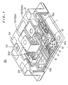
- Fig. 1 is a perspective view, with portions broken away for clarity, of a semiconductor device 30 of a preferred embodiment according to the present invention.
- Fig. 2 is a plan view showing a quarter of a power module 10 included in the semiconductor device 30. A portion shown in Fig. 2 is equivalent to a unit module 10a.
- the power module 10 of Fig. 1 includes four unit modules 10a to 10d.
- the power module 10 is fixed on a copper base plate 1.
- Main electrode terminals 32 (32a, 32b) and a control electrode terminal 33 are mounted upright on the upper surface of the power module 10.
- the power module 10 is located in the bottom of the semiconductor device 30, and is housed in a case 31.
- the case 31 may be an insert case or an outsert case.
- the "insert case” means a case to which the electrode terminals 32, 33 have been previously attached, and the “outsert case” means a case to which the electrode terminals 32, 33 are attached as the case 31 is mounted to the copper base plate 1.
- the case 31 has the shape of an open-bottomed box, the lower end thereof being soldered to the peripheral portion of the metal base plate 1. Resin is introduced into the case 31 through a hole 34 formed on the top of the case 31, and is heated to harden, whereby the power module 10 and the electrode terminals 32, 33 are sealed.
- Fig. 3 is a cross-sectional view taken along the line A-A of Fig. 2.
- the power module 10 includes a first composite substrate (laminate) 5 disposed on the upper major surface of the metal base plate 1.
- the first composite substrate 5 includes a ceramic insulating substrate 3 made principally of Al 2 O 3 or AlN, a copper pattern 4 deposited on the upper major surface of the ceramic insulating substrate 3, and a copper layer 2 deposited almost over the lower major surface of the ceramic insulating substrate 3.
- Fig. 4 shows only the first composite substrate 5 on the metal base plate 1 in plan view.
- the copper pattern 4 is roughly divided into four regions 4a to 4e.
- the broken line of Fig. 4 is a phantom line conceptually showing the boundary between the region 4a and the regions 4b to 4d.
- the region 4a is continuous with the regions 4b to 4d.
- the first region 4a is a strip-shaped region extending in a direction X parallel to the upper major surface of the metal base plate 1.
- the second regions 4b, 4c are of peninsular configuration extending from a side face of the first region 4a in a direction Y substantially perpendicular to the direction X.
- a slit 70 is formed between the second regions 4b and 4c. The slit 70 extends in the Y direction, and the deepest portion thereof reaches the side face of the first region 4a.
- the third region 4d extends from an end of the first region 4a in the Y direction.
- a slit 71 is formed between the third region 4d and the second region 4b.
- the fourth region 4e is provided in a position isolated from the first to third regions 4a to 4d.
- a second composite substrate 9 is provided on the upper major surface of the first region 4a (Fig. 4) of the conductive pattern 4 of the first composite substrate 5.
- the second composite substrate 9 includes a ceramic insulating substrate 7 made principally of Al 2 O 3 or AlN, a copper pattern 8 deposited almost over the upper major surface of the ceramic insulating substrate 7, and a copper layer 6 deposited almost over the lower major surface of the ceramic insulating substrate 7.
- the plan size of the second composite substrate 9 is smaller than that of the first composite substrate 5 and is generally equivalent to that of the first region 4a (Fig. 4) of the conductive pattern 4.
- Fig. 5 is a plan view of the second composite substrate 9.
- the copper layer 8 is a copper strip extending in the X direction.
- the copper layer 6 not shown in Fig. 5 on the lower major surface of the ceramic insulating substrate 7 is also a copper strip extending in the X direction.
- the thickness of the copper patterns 4, 8 and the copper layers 2, 6 is selected from the range of 0.1 to 0.5 mm, respectively.
- the spacing between the copper pattern 4 and the copper layer 2 and the spacing between the copper pattern 8 and the copper layer 6 are preferably selected from the range of 0.5 to 1.5 mm. This is achieved by selecting the thickness of the respective ceramic insulating substrates 3, 6 from the range of 0.5 to 1.5 mm.
- a plurality of power semiconductor chips 12 and a plurality of flywheel diode chips 11 are soldered onto the second regions 4b, 4c of the copper pattern.
- the power semiconductor chips 12 are IGBTs (insulated gate bipolar transistors) each of which has emitter and gate exposed on the upper major surface thereof and a collector exposed on the lower major surface thereof.
- Each of the flywheel diode chips 11 has a cathode exposed on the upper major surface thereof and an anode exposed on the lower major surface thereof.
- One power semiconductor chip 12 and two flywheel diode chips 11 make one set, and a plurality of sets of chips 12, 11 are spaced in the X direction.
- Aluminum wires 13 extending substantially in the Y direction are laid between the copper pattern 8 of the second composite substrate 9 and the upper major surface (cathode) of the flywheel diode chips 11, between the copper pattern 8 and the emitter on the upper major surface of the power semiconductor chips 12, and between the fourth region 4e of the copper pattern 4 and the gate on the upper major surface of the power semiconductor chips 12.
- the aluminum wires associated with the semiconductor chips 11, 12 illustrated on the upper side of Fig. 2 are not shown in Fig. 2.
- Fig. 6 is an equivalent circuit diagram of the unit module 10a of the present preferred embodiment having such wiring.
- an area 14a is defined in a (+X)-side end portion of the copper pattern 8.
- the main electrode terminal 32a of Fig. 1 is connected to the area 14a.
- An area 14b is defined in the third region 4d of the copper pattern 4.
- the main electrode terminal 32b of Fig. 1 is connected to the area 14b.
- the lower structure of the main electrode terminal 32b is not shown in Fig. 1.
- An area 14c is defined in a (+X)-side portion of the fourth region 4e of the copper pattern 4 of Fig. 2.
- the control electrode terminal 32a of Fig. 1 is connected electrically to the area 14c.
- the other unit modules 4b to 4d of Fig. 1 have the same structure as the unit module 4a.
- a positive voltage is applied to the main electrode terminal 32b of Fig. 1, and a negative voltage is applied to the main electrode terminal 32a.
- a control voltage which is positive to the main electrode terminal 32a is applied to the control electrode terminal 33. Then the power semiconductor chips 12 turn on. A current flow at this time will be described hereinafter.
- Fig. 7 is a plan view, with portions of the upper structure of Fig. 2 broken away.
- Fig. 8 shows a current flow of Fig. 1.
- the arrows 15 and 16 of Figs. 7 and 8 indicate the paths of input and output currents, respectively, when the power semiconductor chips 12 conduct in the forward direction.
- the input current flowing from the main electrode terminal 32b is directed from the area 14b of Fig. 2 to the third region 4d of the conductive pattern 4, and then reaches the first region 4a.
- the input current entering the first region 4a flows in the first region 4a in the (-X) direction. Since the copper layer 6 (Fig. 3) on the reverse side of the second composite substrate is soldered to the first region 4a, the input current flows in the copper layer 6 in the (-X) direction.
- the input current changes its direction to the (+Y) direction as it reaches the boundary between the first region 4a and the second regions 4b, 4c, to flow into the second regions 4b, 4c.
- the input current flowing in the second regions 4b, 4c in the (+Y) direction flows into the lower major surface or the collector of the power semiconductor chips 12.
- Such input current path is shown as the path 15.
- the output current flowing out of the emitter on the upper major surface of the power semiconductor chips 12 is directed through the aluminum wires 13 to the copper pattern 8. Since the aluminum wires 13 extend substantially in the Y direction, the output current is antiparallel to the input current flowing in the second regions 4b, 4c.
- the output current changes its direction to the (+X) direction as it reaches the copper pattern 8 through the aluminum wires 13.
- the output current flows to the area 14a in the (+X) direction, and then flows to the exterior from the area 14a through the main electrode terminal 32a.
- the direction of the input current flowing in the first region 4a of the copper pattern 4 is antiparallel to that of the output current flowing in the copper pattern 8. That is, the input current flows in the (-X) direction and the output current flows in the (+X) direction in these portions. This provides for a small inductance of the main current path in these portions.
- the copper pattern 8 is disposed just above the first region 4a, great effects to reduce the floating inductance are provided.
- the aluminum wires 13 and the second peninsular regions 4b, 4c enable the reduction in floating inductance by the antiparallel combination of "lines” (wires 13) and "planes" (regions 4b, 4c).
- the first region 4a of the copper pattern 4 and the copper pattern 8 enable the reduction in floating inductance by the antiparallel combination of a "plane” (copper pattern 8) and a "plane” (region 4a).
- the use of both combinations affords remarkable effects to reduce the floating inductance in the semiconductor device 30 of the present invention.
- the slit 70 is located between two pairs of semiconductor chips, and the slit 71 is located between the second region 4b and the third region 4d of the copper pattern 4.
- Fig. 9 shows a structure wherein the slits 70, 71 are absent.
- a copper pattern 4m is of rectangular configuration, and the area 14b to be connected to the main electrode terminal 32b of Fig. 1 is defined in an end portion of the copper pattern 4m.
- Regions 12a represent positions in which the semiconductor chips 12 and the like are to be mounted.
- the current path 15 of the input current does not run just under the copper pattern 8 of the second composite substrate 9.
- the current path 15 runs in oblique directions.
- the semiconductor device of the present preferred embodiment of Fig. 2 having the slits 70, 71 is capable of forcing the input current path 15 to run in the (-X) direction (Fig. 7) and then to change its direction to the (+Y) direction so as to provide an L-shaped path. Furthermore, the input current path 15 runs adjacent the output current path 16, providing great effects to cancel the magnetic fields mutually.
- the semiconductor device 30 is fabricated, for example, in a manner to be described hereinafter.
- First prepared is the first composite substrate 5 including the insulating substrate 3, the copper pattern 4 deposited on the upper major surface of the insulating substrate 3, and the copper layer 2 deposited on the lower major surface of the insulating substrate 3. Also prepared is the second composite substrate 9 including the insulating substrate 7, the copper pattern 8 deposited on the upper major surface of the insulating substrate 7, and the copper layer 6 deposited on the lower major surface of the insulating substrate 7. The size of the second composite substrate 9 is determined in accordance with the size of the first region 4a of the copper pattern 4 of the first composite substrate 5.
- the first composite substrate 5 is joined to the upper major surface of the metal base plate 1 such that the copper layer 2 is positioned in face-to-face relation to the upper major surface of the metal base plate 1.
- the second composite substrate 9 is joined onto the first region 4a of the copper pattern 4 of the first composite substrate 5.
- the junction may be made by means of direct-connect process or activated metal process. Specifically, the junction is achieved by high-temperature brazing using hard solder or by using, as junction layers, copper oxide provided by heating the copper layers 2, 4, 6, 8 in an atmosphere of oxygen.
- Fig. 10 shows the power module after the junction.
- the metal base plate 1, the first laminate 5, and the second laminate 9 are joined together with junction layers 18, 17.
- the flywheel diode chips 11 and the power semiconductor chips 12 are soldered onto the second regions 4b, 4c of the copper pattern 4.
- the wires 13 are laid between the semiconductor chips 11, 12 and the copper patterns 8, 4e to bond the ends of the wires 13 to the semiconductor chips 11, 12 and the copper patterns 8, 4e.
- the power module provided in the foregoing manner is housed in the case 31 (Fig. 1). Almost simultaneously, the electrode terminals 32, 33 (Fig. 1) are joined to the corresponding areas 14a to 14d (Fig. 2).
- Resin is introduced into the case 31 through the hole 34 formed in the upper surface of the case 31, and is then heated to harden.
- the semiconductor chips 11, 12, the wires 13 and their vicinities may be protected with silicon gel or the like.
Abstract
Description
- The present invention relates to a semiconductor device and a method of fabricating the Same. More particularly, the invention relates to a semiconductor device having a reduced floating inductance and a method of fabricating the same.
- Fig. 15 shows a
conventional composite substrate 50 with thick copper foil for a power module in top plan view, in cross section and in bottom plan view. - The
composite substrate 50 includes a ceramicinsulating substrate 51, acircuit pattern 52 deposited on one surface of the ceramicinsulating substrate 51, and aback pattern 53 deposited on the other surface thereof. - In Fig. 16, there is shown, in perspective, a
conventional semiconductor device 60 including thecomposite substrate 50. Thesemiconductor device 60 comprises acopper base plate 1, thecomposite substrate 50, apower semiconductor element 12,aluminum wires 13,main electrode terminals 62, acontrol electrode terminal 63, and acase 61. - Fig. 17 shows a main
current path 64 of thesemiconductor device 60 in practical use. It will be apparent from the comparison between Figs. 16 and 17 that the maincurrent path 64 from one of themain electrode terminals 62 leads to thesemiconductor chips 12, and then runs through thewires 13 and part of thecircuit pattern 52 to exit at anothermain electrode terminal 62. - Such semiconductor device is used as a power switching device while repeating ON/OFF operation. As MOS power devices have been recently put to practical use, the switching time is very rapid, commonly in the range of 20 to 30 KHz. The switching frequency is expected to increase acceleratedly.
- As the switching time becomes short, the rate of current change per time di/dt rises in ON-to-OFF and OFF-to-ON operation. This causes a surge voltage V = L·dildt in ON-to-OFF operation due to a floating inductance L present in the main
current path 64. Increase in floating inductance L results in increase in surge voltage. When the increasing surge voltage exceeds the rating of thepower semiconductor elements 12, thepower semiconductor elements 12 break down. - EP-A-0 427 143 discloses a semiconductor power device wherein a ceramic substrate is coated with a metallic coating. A first metallic layer is provided on the metallic coating and is divided into an auxiliary emitter area and a positive terminal area (figure 3). A further ceramic isolating layer is arranged on the auxiliary emitter area and carries a gate area. Further, an isolating layer is arranged on the positive terminal area and is covered with a tap connection layer. A plurality of transistor chips is provided on the tap connection area which furthermore carries a negative terminal connection layer on which further isolating and electrically conducting layers are provided. Bonding wires provide the necessary internal connection between the components.
- EP-A-0 277 546 discloses a semiconductor device including at least one semiconductor chip wherein the terminal connectors are arranged side by side in close proximity and at least partially parallel to each other. The terminal connectors are connected with metallic connectors arranged on an isolating substrate. The connectors include portions extending at right angles to each other, and are connected, via bonding wires, to the respective electrodes of the semiconductor chips provided on metallic layers on the substrate.
- An object of the present invention is to provide a semiconductor device wherein a surge voltage produced in ON-to-OFF operation is not increased with an increase in switching frequency being used so that a semiconductor element is not broken down.
- Another object of the invention is to provide a method of fabricating the above-mentioned semiconductor device.
- These objects are achieved by the features stated in the independent Claims.
- In the semiconductor device, the input and output currents flow in the first and second conductive layers in antiparallel with each other, so that the respective magnetic fields generated by the input and output currents cancel each other. As a result, a floating inductance decreases, and a high surge voltage is not produced.
- When the at least one semiconductor chip includes a plurality of semiconductor chips spaced in the first direction, it is preferable that there is provided a slit substantially parallel to the second direction in a portion corresponding to the spacing in the second region.
- In the semiconductor device the second region of the second conductive layer on which the semiconductor chip is disposed is of peninsular configuration. The input or output current flows in the second direction in which the peninsula extends.
- The input current, by way of example, flowing in the first region in the first direction maintains its flowing direction up to the boundary between the first region and the second peninsular region. The input current changes its flowing direction to the second direction at the boundary, and then flows into the semiconductor chip in the second direction.
- The output current from the semiconductor chip reaches the fourth conductive layer from the second peninsular region and flows in the fourth conductive layer in the third direction which is antiparallel to the first direction of the input current.
- If the second region is not peninsular in configuration, the input current has a component which flows in the first region at a finite angle with respect to the first direction. Since the maximum effect to reduced the floating inductance is achieved when the input and output currents are completely antiparallel to each other, the peninsular shape of the second region enables the inductance reduction effect to be particularly enhanced.
- The slit is formed in the portion corresponding to the spacing between the semiconductor chips, if in plurality, in the second region. This enhances the effect to cause the output or input current in the second region to flow in the third direction.
- The semiconductor device according to the present invention is not broken down if the switching frequency being used is increased.
- These and other objects, features, aspects and advantages of the present invention will become more apparent from the following detailed description of the present invention when taken in conjunction with the accompanying drawings.
- Fig. 1 is a cross-sectional view, with portions broken away, of a semiconductor device of a preferred embodiment according to the present invention:
- Fig. 2 is a partial plan view of a power module included in the semiconductor device of Fig. 1;
- Fig. 3 is a cross-sectional view of the power module taken along the line A-A of Fig. 2;
- Fig. 4 is a partial plan view of a first composite substrate of the power module of Fig. 2;
- Fig. 5 is a partial plan view of a second composite substrate of the power module of Fig. 2;
- Fig. 6 is a circuit diagram of the power module of Fig. 2;
- Fig. 7 shows a current path in the power module of Fig. 2;
- Fig. 8 shows a current path in the semiconductor device of Fig. 1;
- Fig. 9 shows a comparable example of the power module of Fig. 2;
- Fig. 10 is a cross-sectional view showing a fabrication process of the power module of Fig. 2;
- Fig. 11 is a cross-sectional view showing another fabrication process of the power module of Fig. 2;
- Fig. 12 is a partial plan view of a power module included in a semiconductor device of another preferred embodiment according to the present invention;
- Fig. 13 is a cross-sectional view of the power module taken along the line B-B of Fig. 12;
- Fig. 14 shows a current path in the power module of Fig. 12;
- Fig. 15 shows a composite substrate with thick copper foil for use in a conventional semiconductor device;
- Fig. 16 is a perspective view, with portions broken away, of the conventional semiconductor device; and
- Fig. 17 shows a current path in the semiconductor device of Fig. 16.
- Fig. 1 is a perspective view, with portions broken away for clarity, of a
semiconductor device 30 of a preferred embodiment according to the present invention. Fig. 2 is a plan view showing a quarter of apower module 10 included in thesemiconductor device 30. A portion shown in Fig. 2 is equivalent to aunit module 10a. Thepower module 10 of Fig. 1 includes fourunit modules 10a to 10d. - Referring to Fig. 1, the
power module 10 is fixed on acopper base plate 1. Main electrode terminals 32 (32a, 32b) and acontrol electrode terminal 33 are mounted upright on the upper surface of thepower module 10. - The
power module 10 is located in the bottom of thesemiconductor device 30, and is housed in acase 31. Thecase 31 may be an insert case or an outsert case. The "insert case" means a case to which theelectrode terminals electrode terminals case 31 is mounted to thecopper base plate 1. - The
case 31 has the shape of an open-bottomed box, the lower end thereof being soldered to the peripheral portion of themetal base plate 1. Resin is introduced into thecase 31 through ahole 34 formed on the top of thecase 31, and is heated to harden, whereby thepower module 10 and theelectrode terminals - Fig. 3 is a cross-sectional view taken along the line A-A of Fig. 2.
- Referring to Figs. 2 and 3, the
power module 10 includes a first composite substrate (laminate) 5 disposed on the upper major surface of themetal base plate 1. The firstcomposite substrate 5 includes a ceramic insulatingsubstrate 3 made principally of Al2O3 or AlN, acopper pattern 4 deposited on the upper major surface of the ceramic insulatingsubstrate 3, and acopper layer 2 deposited almost over the lower major surface of the ceramic insulatingsubstrate 3. - Fig. 4 shows only the first
composite substrate 5 on themetal base plate 1 in plan view. As shown in Fig. 4, thecopper pattern 4 is roughly divided into four regions 4a to 4e. The broken line of Fig. 4 is a phantom line conceptually showing the boundary between the region 4a and theregions 4b to 4d. In practice, the region 4a is continuous with theregions 4b to 4d. - The first region 4a is a strip-shaped region extending in a direction X parallel to the upper major surface of the
metal base plate 1. Thesecond regions slit 70 is formed between thesecond regions slit 70 extends in the Y direction, and the deepest portion thereof reaches the side face of the first region 4a. - The
third region 4d extends from an end of the first region 4a in the Y direction. Aslit 71 is formed between thethird region 4d and thesecond region 4b. - The
fourth region 4e is provided in a position isolated from the first to third regions 4a to 4d. - Referring again to Figs. 2 and 3, a second
composite substrate 9 is provided on the upper major surface of the first region 4a (Fig. 4) of theconductive pattern 4 of the firstcomposite substrate 5. The secondcomposite substrate 9 includes a ceramic insulatingsubstrate 7 made principally of Al2O3 or AlN, acopper pattern 8 deposited almost over the upper major surface of the ceramic insulatingsubstrate 7, and acopper layer 6 deposited almost over the lower major surface of the ceramic insulatingsubstrate 7. - The plan size of the second
composite substrate 9 is smaller than that of the firstcomposite substrate 5 and is generally equivalent to that of the first region 4a (Fig. 4) of theconductive pattern 4. Fig. 5 is a plan view of the secondcomposite substrate 9. Thecopper layer 8 is a copper strip extending in the X direction. Thecopper layer 6 not shown in Fig. 5 on the lower major surface of the ceramic insulatingsubstrate 7 is also a copper strip extending in the X direction. - Preferably, the thickness of the
copper patterns copper pattern 4 and thecopper layer 2 and the spacing between thecopper pattern 8 and thecopper layer 6 are preferably selected from the range of 0.5 to 1.5 mm. This is achieved by selecting the thickness of the respective ceramic insulatingsubstrates - Referring again to Figs. 2 and 3, a plurality of power semiconductor chips 12 and a plurality of
flywheel diode chips 11 are soldered onto thesecond regions - One
power semiconductor chip 12 and twoflywheel diode chips 11 make one set, and a plurality of sets ofchips -
Aluminum wires 13 extending substantially in the Y direction are laid between thecopper pattern 8 of the secondcomposite substrate 9 and the upper major surface (cathode) of theflywheel diode chips 11, between thecopper pattern 8 and the emitter on the upper major surface of the power semiconductor chips 12, and between thefourth region 4e of thecopper pattern 4 and the gate on the upper major surface of the power semiconductor chips 12. The aluminum wires associated with the semiconductor chips 11, 12 illustrated on the upper side of Fig. 2 are not shown in Fig. 2. - Fig. 6 is an equivalent circuit diagram of the
unit module 10a of the present preferred embodiment having such wiring. - Referring to Fig. 2, an
area 14a is defined in a (+X)-side end portion of thecopper pattern 8. Themain electrode terminal 32a of Fig. 1 is connected to thearea 14a. Anarea 14b is defined in thethird region 4d of thecopper pattern 4. Themain electrode terminal 32b of Fig. 1 is connected to thearea 14b. The lower structure of themain electrode terminal 32b is not shown in Fig. 1. - An
area 14c is defined in a (+X)-side portion of thefourth region 4e of thecopper pattern 4 of Fig. 2. Thecontrol electrode terminal 32a of Fig. 1 is connected electrically to thearea 14c. - The
other unit modules 4b to 4d of Fig. 1 have the same structure as the unit module 4a. - A positive voltage is applied to the
main electrode terminal 32b of Fig. 1, and a negative voltage is applied to themain electrode terminal 32a. A control voltage which is positive to themain electrode terminal 32a is applied to thecontrol electrode terminal 33. Then the power semiconductor chips 12 turn on. A current flow at this time will be described hereinafter. - Fig. 7 is a plan view, with portions of the upper structure of Fig. 2 broken away. Fig. 8 shows a current flow of Fig. 1. The
arrows - The input current flowing from the
main electrode terminal 32b is directed from thearea 14b of Fig. 2 to thethird region 4d of theconductive pattern 4, and then reaches the first region 4a. The input current entering the first region 4a flows in the first region 4a in the (-X) direction. Since the copper layer 6 (Fig. 3) on the reverse side of the second composite substrate is soldered to the first region 4a, the input current flows in thecopper layer 6 in the (-X) direction. - The input current changes its direction to the (+Y) direction as it reaches the boundary between the first region 4a and the
second regions second regions - The input current flowing in the
second regions - Such input current path is shown as the
path 15. - On the other hand, the output current flowing out of the emitter on the upper major surface of the power semiconductor chips 12 is directed through the
aluminum wires 13 to thecopper pattern 8. Since thealuminum wires 13 extend substantially in the Y direction, the output current is antiparallel to the input current flowing in thesecond regions - It is well known in the art of electromagnetism that the floating inductance of go and return parallel conductor is in general low. For this reason, the current path formed by the
second regions aluminum wires 13 serves as a small path of floating inductance. - The output current changes its direction to the (+X) direction as it reaches the
copper pattern 8 through thealuminum wires 13. The output current flows to thearea 14a in the (+X) direction, and then flows to the exterior from thearea 14a through themain electrode terminal 32a. - The direction of the input current flowing in the first region 4a of the
copper pattern 4 is antiparallel to that of the output current flowing in thecopper pattern 8. That is, the input current flows in the (-X) direction and the output current flows in the (+X) direction in these portions. This provides for a small inductance of the main current path in these portions. In particular, since thecopper pattern 8 is disposed just above the first region 4a, great effects to reduce the floating inductance are provided. - The
aluminum wires 13 and thesecond peninsular regions regions copper pattern 4 and thecopper pattern 8 enable the reduction in floating inductance by the antiparallel combination of a "plane" (copper pattern 8) and a "plane" (region 4a). The use of both combinations affords remarkable effects to reduce the floating inductance in thesemiconductor device 30 of the present invention. - The
semiconductor device 30 that has a low floating inductance of the main current path for the above-mentioned reasons has a small surge voltage V=L·di/dt if the rate of current change di/dt rises in ON-to-OFF and OFF-to-ON operations due to increasing switching frequency being used. Thus the power semiconductor chips 12 are effectively prevented from being broken down. - The reason for provision of the
slits - The
slit 70 is located between two pairs of semiconductor chips, and theslit 71 is located between thesecond region 4b and thethird region 4d of thecopper pattern 4. - For explanation of the functions of the
slits slits slits copper pattern 4m is of rectangular configuration, and thearea 14b to be connected to themain electrode terminal 32b of Fig. 1 is defined in an end portion of thecopper pattern 4m.Regions 12a represent positions in which the semiconductor chips 12 and the like are to be mounted. - In the case of Fig. 9, the
current path 15 of the input current does not run just under thecopper pattern 8 of the secondcomposite substrate 9. In addition, thecurrent path 15 runs in oblique directions. Thus the input and output currents are not completely antiparallel to each other, and the distance between the input and output currents is long, resulting in less effective reduction in floating inductance. - The semiconductor device of the present preferred embodiment of Fig. 2 having the
slits current path 15 to run in the (-X) direction (Fig. 7) and then to change its direction to the (+Y) direction so as to provide an L-shaped path. Furthermore, the inputcurrent path 15 runs adjacent the outputcurrent path 16, providing great effects to cancel the magnetic fields mutually. - The
semiconductor device 30 is fabricated, for example, in a manner to be described hereinafter. - First prepared is the first
composite substrate 5 including the insulatingsubstrate 3, thecopper pattern 4 deposited on the upper major surface of the insulatingsubstrate 3, and thecopper layer 2 deposited on the lower major surface of the insulatingsubstrate 3. Also prepared is the secondcomposite substrate 9 including the insulatingsubstrate 7, thecopper pattern 8 deposited on the upper major surface of the insulatingsubstrate 7, and thecopper layer 6 deposited on the lower major surface of the insulatingsubstrate 7. The size of the secondcomposite substrate 9 is determined in accordance with the size of the first region 4a of thecopper pattern 4 of the firstcomposite substrate 5. - The first
composite substrate 5 is joined to the upper major surface of themetal base plate 1 such that thecopper layer 2 is positioned in face-to-face relation to the upper major surface of themetal base plate 1. The secondcomposite substrate 9 is joined onto the first region 4a of thecopper pattern 4 of the firstcomposite substrate 5. - The junction may be made by means of direct-connect process or activated metal process. Specifically, the junction is achieved by high-temperature brazing using hard solder or by using, as junction layers, copper oxide provided by heating the copper layers 2, 4, 6, 8 in an atmosphere of oxygen.
- Fig. 10 shows the power module after the junction. The
metal base plate 1, thefirst laminate 5, and thesecond laminate 9 are joined together withjunction layers 18, 17. - The
flywheel diode chips 11 and the power semiconductor chips 12 are soldered onto thesecond regions copper pattern 4. Thewires 13 are laid between the semiconductor chips 11, 12 and thecopper patterns wires 13 to the semiconductor chips 11, 12 and thecopper patterns - The power module provided in the foregoing manner is housed in the case 31 (Fig. 1). Almost simultaneously, the
electrode terminals 32, 33 (Fig. 1) are joined to the correspondingareas 14a to 14d (Fig. 2). - Resin is introduced into the
case 31 through thehole 34 formed in the upper surface of thecase 31, and is then heated to harden. The semiconductor chips 11, 12, thewires 13 and their vicinities may be protected with silicon gel or the like. -
- (1) A laminate including two insulating substrates may be deposited on the
metal base plate 1 in place of the twocomposite substrates
The present invention may be accomplished, for example, by joining a laminate 19 including threecopper patterns substrates metal base plate 1 withsolder 18, as shown in Fig. 11.
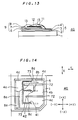
In this case, it is preferable that the thickness of therespective metal patterns copper patterns - (2) Although the input current path is on the lower side and the output current path is on the upper side in the
power module 10 of the above-mentioned preferred embodiment, the input current path may be on the upper side whereas the output current path is on the lower side. Fig. 12 is a plan view of apower module 40 in such case, and Fig. 13 is a cross-sectional view taken along the line B-B of Fig. 12. Fig. 14 shows current paths in thepower module 40, with portions of the upper structure of Fig. 12 broken away.
Thecopper pattern 4 formed on the upper major surface of the firstcomposite substrate 5 includes, as shown in Fig. 14, the first region 4a extending in the X direction, thesecond peninsular regions third region 4d in which thearea 14c (Fig. 12) for connection of the terminal is defined.Slits 72 are formed between theregions
The secondcomposite substrate 9 having a plan size smaller than the firstcomposite substrate 5 is joined onto the firstcomposite substrate 5. Thecopper pattern 6 formed on the lower major surface of the secondcomposite substrate 9 is adapted to fit thecopper pattern 4.
Thecopper pattern 8 is formed on the upper major surface of the secondcomposite substrate 9. Thecopper pattern 8 includes aregion 8a (Fig. 14) extending in the X direction,regions region 8a in the Y direction, aregion 8d extending parallel to theregion 8b, and aregion 8e isolated from theregions 8a to 8d.Slits 73 are formed between theregions
The semiconductor chips 11, 12 (Fig. 12) are joined onto theregions wires 13 extending in the Y direction connect the semiconductor chips 11, 12 to thecopper patterns power module 40 are identical with those of thepower module 10 of Fig. 2.
In thepower module 40 of Figs. 12 to 14, an input current 41 from thearea 14b (Fig. 12) flows in theregion 8d (Fig. 14) in the (-Y) direction, and then flows in theregion 8a in the (-X) direction. The input current changes its direction to the (+Y) direction at the boundary between theregion 8a and theregions regions
The output current from the upper major surface of the power semiconductor chips 12 flows through thewires 13 to thecopper pattern regions composite substrate 5. The output current further flows in thecopper pattern regions path 42 in dotted lines. The output current changes its direction to the (+X) direction, and flows in the copper pattern region 4a of the firstcomposite substrate 5 just under thecopper pattern region 8a of the secondcomposite substrate 9 in the (+X) direction.
The output current changes its direction to the (+Y) direction as it reaches thecopper pattern region 4d to flow out from thearea 14c (Fig. 12) to the main electrode terminal.
In thepower module 40, the input and outputcurrent paths slits power module 10 of Fig. 2. - (3) Although the above-mentioned preferred embodiments employ the power module including two insulating substrates, more insulating substrates and copper patterns may be used. In such case, the input and output current paths may be adapted to be antiparallel to each other. The copper patterns may be replaced with other conductive patterns such as aluminum patterns.
- While the invention has been shown and described in detail, the foregoing description is in all aspects illustrative and not restrictive. It is therefore understood that numerous modifications and variations can be devised without departing from the scope of the invention as defined by the appended claims.
Claims (20)
- A semiconductor device for controlling an input current by a semiconductor chip to provide an output current, comprising:(a) a metal base plate (1) having a major surface;(b) a first insulating substrate (3) disposed on said major surface of said metal base plate;(c) a first conductive layer (4) provided on said first insulating substrate and having(c-1) a first region (4a) for conducting one of said input and output currents in a first direction (X) parallel to said major surface, and(c-2) a second peninsular region (4b, 4c) continuous with said first region and protruding therefrom in a second direction (Y) different from said first direction (X) on said major surface;(d) a second insulating substrate (7) provided on said first conductive layer (4) except at least an end portion of said second region (4b, 4c);(e) a second conductive layer (8) provided on said second insulating substrate (7) and having a third region (8a) for conducting the other current in a third direction antiparallel to said first direction, said third region (8a) overlaying said first region (4a) of said first conductive layer (4); and(f) at least one semiconductor chip (12) provided on said second region (4b, 4c) or said second conductive layer (8) and connected electrically to said second region (4b, 4c) and said second conductive layer.
- The semiconductor device of claim 1, wherein
(f-1) a plurality of semiconductor chips (12) are provided on said second region (4b, 4c) and spaced in said first direction, and
there is provided a slit (70) substantially parallel to said second direction in a portion corresponding to said spacing in said second region. - The semiconductor chip of claim 2, further comprising:(g) a first electrode (32b) connected electrically to an end of said first region (4a); and(h) a second electrode (32a) connected electrically to an end of said second conductive layer located on the same side as said end of said first region.
- The semiconductor device of anyone of the preceding claims, further comprising:
(i) a third conductive layer (2) provided between said metal base plate (1) and said first insulating substrate (3). - The semiconductor device of anyone of the preceding claims, wherein the respective thickness of said first and second conductive layers (4, 8) is selected from the range of 0.1 to 0.5 mm.
- The semiconductor device of any of claims 1 to 4, wherein a spacing between said first and second conductive layers (4, 8) is selected from the range of 0.5 to 1.5 mm.
- The semiconductor device of anyone of the preceding claims, wherein said first and second conductive layers (4, 8) are formed substantially of copper.
- The semiconductor device of anyone of the preceding claims, further comprising:
(g) at least one wire (13) electrically connecting each upper surface of said at least one semiconductor chip (12) and one of said second region (4b, 4c) and said second conductive layer (8) to conduct one of said input and output currents, and extending substantially in said second direction. - The semiconductor device of claim 8, whereinsaid at least one first semiconductor chip (12) includes:(f-1) at least one first chip (12) provided on said second region (4b, 4c); and(f-2) at least one second chip (12) provided on said second conductive layer (8); andeach one of said at least one wire (13) includes:(g-1) a first end connected electrically to one of upper surfaces of said at least one first chip (12); and(g-2) a second end connected electrically to one upper surfaces of said at least one second chip (12).
- The semiconductor device of anyone of the preceding claims, whereinsaid second conductive layer (8) further includes:
(e-1) a fourth peninsular region (8b, 8c) continuous with said third region (8a) and protruding in said second direction (Y) to overlay said second region (4b, 4c) except said end portion thereof,said at least one semiconductor chip (12) includes:
(f-1) a plurality of semiconductor chips provided on said fourth peninsular region and spaced in said third direction, andthere is provided a slit (73) substantially parallel to said third direction in a portion corresponding to said spacing in said fourth peninsular region. - A method of fabricating a semiconductor device for controlling an input current by a semiconductor chip to provide an output current, said method comprising the steps of:(a) providing a laminate (19) including a first insulating substrate (3), a first conductive layer (4), a second insulating substrate (7) and a second conductive layer (8) joined together in this order, said first and second conductive layers (4, 8) being at least partially exposed, respectively;(b) fixing said laminate (19) on a major surface of a metal base plate (1); and(c) fixing a semiconductor chip (12) on an upper surface of said exposed first or second conductive layer (4, 8) of said laminate,said first conductive layer (4) including a first region (4a) for conducting one of said input and output currents in a first direction (X) parallel to said major surface, and a second peninsular region (4b, 4c) continuous with said first region and protruding in a second direction (Y) different from said first direction on said major surface,said second insulating substrate (7) being provided on said first conductive layer (4) except at least an end portion of said second region (4b, 4c),said second conductive layer (8) being provided on said second insulating substrate (7) and having a portion for conducting the other current in a third direction antiparallel to said first direction (X), said portion overlaying said first region (4a) of said first conductive layer (4).
- The method of claim 11, whereinsaid step (a) includes the steps of:(a-1) providing said first insulating substrate (3);(a-2) selectively providing said first conductive layer (4) on said first insulating substrate (3);(a-3) selectively providing said second insulating substrate (7) on said first conductive layer (4); and(a-4) providing said second conductive layer (8) on said second insulating substrate, andsaid step (a-4) includes the steps of:(a-4-1) providing a conductive strip smaller in plan size than said first conductive layer (4); and(a-4-2) fixing said conductive strip on said second insulating substrate (7), with the length of said conductive strip directed in said second direction (Y), to provide said second conductive layer (8).
- The method of claim 12, further comprising the steps of:(d) providing a first electrode (32b) to electrically connect an end of said first conductive layer (4) to said first electrode; and(e) providing a second electrode (32a) to electrically connect an end of said second conductive layer (8) located on the same side as said end of said first conductive layer to said second electrode.
- The method of claim 13, whereinsaid step (a-2) includes the step of:
(a-2-1) providing a metal layer having a thickness selected from the range of 0.1 to 0.5 mm to provide said first conductive layer (4), andsaid step (a-4-1) includes the step of:
(a-4-1-1) providing a metal layer having a thickness selected from the range of 0.1 to 0.5 mm to provide said conductive strip. - The method of claim 12, 13 or 14, wherein
said step (a-3) includes the step of:
(a-3-1) fixing said second insulating layer (7) on said first conductive layer (4) such that a spacing between said first and second conductive layers (4, 8) is a value selected from the range of 0.5 to 1,5 mm. - A method of fabricating a semiconductor device for controlling an input current by a semiconductor chip to provide an output current, said method comprising the steps of:(a) providing a first laminate (5) including a first insulating substrate (3) and first and second conductive layers (2, 4) deposited on first and second major surfaces of said first insulating substrate (3), respectively, and a second laminate (9) including a second insulating substrate (7) and third and fourth conductive layers (6, 8) deposited on first and second major surfaces of said second insulating substrate (7), respectively;(b) fixing said first laminate (5) on a major surface of a metal base plate (1) such that said first conductive layer (2) is positioned in face-to-face relation to said major surface of said metal base plate;(c) fixing said second laminate (9) on said first laminate (5) such that said third conductive layer (6) is positioned in face-to-face relation to said second conductive layer (4) and such that a portion of a major surface of said second conductive layer (4) is exposed; and(d) fixing said semiconductor chip (12) on said portion of said major surface of said second conductive layer (4) or on said fourth conductive layer (8),said second conductive layer (4) including a first region (4a) for conducting one of said input and output currents in a first direction (X) parallel to said major surface of said metal base plate (1), and a second peninsular region (4b, 4c) continuous with said first region (4a) and protruding in a second direction different from said first direction on said major surface of said metal base plate (1),said second insulating substrate (7) being provided on said second conductive layer (4) except at least an end portion of said second region (4b, 4c),said fourth conductive layer (8) having a portion for conducting the other current in a third direction antiparallel to said first direction, said portion overlaying said first region (4a) of said second conductive layer (4).
- The method of claim 16, whereinsaid step (a) includes the step of:
(a-1) providing said second laminate (9) so that said second laminate is smaller in plan size than said second conductive layer (4) and is of elongated configuration, andsaid step (b) includes the step of:
(b-1) fixing said second laminate (9) on said first laminate (5), with the length of said second laminate directed in said second direction (Y). - The method of claim 17, further comprising the steps of:(d) electrically connecting a first electrode (32b) to a first end of said second conductive layer (4); and(e) electrically connecting a second electrode (32a) to a second end of said fourth conductive layer (8) located on the same side as said first end of said second conductive layer.
- The method of claim 18, wherein
said step (a-1) includes the steps of:(a-1-1) fixing first and second metal layers each having a thickness selected from the range of 0.1 to 0.5 mm on said first and second major surfaces of said first insulating substrate (3) to provide said first and second conductive layers (2, 4) of said first laminate (5); and(a-1-2) fixing third and fourth metal layers each having a thickness selected from the range of 0.1 to 0.5 mm on said first and second major surfaces of said second insulating substrate (7) to provide said third and fourth conductive layers (6, 8) of said second laminate. - The method of claim 19, wherein
said step (a-1) further includes the steps of:(a-1-3) producing said first laminate (5) such that a spacing between said first and second conductive layers (2, 4) is a value selected from the range of 0.5 to 1.5 mm; and(a-1-4) producing said second laminate (9) such that a spacing between said third and fourth conductive layers (6, 8) is a value selected from the range of 0.5 to 1.5 mm.
Applications Claiming Priority (2)
| Application Number | Priority Date | Filing Date | Title |
|---|---|---|---|
| JP4193979A JP2725954B2 (en) | 1992-07-21 | 1992-07-21 | Semiconductor device and manufacturing method thereof |
| JP193979/92 | 1992-07-21 |
Publications (2)
| Publication Number | Publication Date |
|---|---|
| EP0585578A1 EP0585578A1 (en) | 1994-03-09 |
| EP0585578B1 true EP0585578B1 (en) | 1997-03-12 |
Family
ID=16316963
Family Applications (1)
| Application Number | Title | Priority Date | Filing Date |
|---|---|---|---|
| EP93111381A Expired - Lifetime EP0585578B1 (en) | 1992-07-21 | 1993-07-15 | Semiconductor device with reduced floating inductance and method of fabricating same |
Country Status (5)
| Country | Link |
|---|---|
| US (1) | US5424579A (en) |
| EP (1) | EP0585578B1 (en) |
| JP (1) | JP2725954B2 (en) |
| KR (1) | KR0120918B1 (en) |
| DE (1) | DE69308691T2 (en) |
Families Citing this family (39)
| Publication number | Priority date | Publication date | Assignee | Title |
|---|---|---|---|---|
| JP2988243B2 (en) * | 1994-03-16 | 1999-12-13 | 株式会社日立製作所 | Power hybrid integrated circuit device |
| EP0706221B8 (en) * | 1994-10-07 | 2008-09-03 | Hitachi, Ltd. | Semiconductor device comprising a plurality of semiconductor elements |
| US5569957A (en) * | 1994-10-31 | 1996-10-29 | Harris Corporation | Low inductance conductor topography for MOSFET circuit |
| US6049126A (en) * | 1995-12-14 | 2000-04-11 | Nec Corporation | Semiconductor package and amplifier employing the same |
| JP3480771B2 (en) * | 1995-12-20 | 2003-12-22 | 三菱電機株式会社 | Semiconductor device |
| JP3168901B2 (en) * | 1996-02-22 | 2001-05-21 | 株式会社日立製作所 | Power semiconductor module |
| US6954368B1 (en) | 1996-07-22 | 2005-10-11 | HYDRO-QUéBEC | Low stray interconnection inductance power converting molecule for converting a DC voltage into an AC voltage, and a method therefor |
| US6078501A (en) * | 1997-12-22 | 2000-06-20 | Omnirel Llc | Power semiconductor module |
| US6069403A (en) * | 1998-10-06 | 2000-05-30 | Intersil Corporation | Power module with lowered inductance and reduced voltage overshoots |
| JP4475757B2 (en) * | 2000-07-19 | 2010-06-09 | 京セラ株式会社 | Inverter control module |
| JP3635012B2 (en) * | 2000-07-26 | 2005-03-30 | 京セラ株式会社 | Inverter control module |
| JP4475773B2 (en) * | 2000-08-11 | 2010-06-09 | 京セラ株式会社 | Inverter control module |
| DE10107609A1 (en) * | 2001-02-17 | 2002-08-29 | Power One Ag Uster | Power Module |
| DE10294631D2 (en) | 2001-09-28 | 2004-10-07 | Siemens Ag | Arrangement with power semiconductor components for power control of high currents and application of the arrangement |
| JP2003258179A (en) * | 2002-02-28 | 2003-09-12 | Sanyo Electric Co Ltd | Semiconductor device and manufacturing method therefor |
| US6844621B2 (en) * | 2002-08-13 | 2005-01-18 | Fuji Electric Co., Ltd. | Semiconductor device and method of relaxing thermal stress |
| US7327024B2 (en) * | 2004-11-24 | 2008-02-05 | General Electric Company | Power module, and phase leg assembly |
| JP2006253516A (en) * | 2005-03-14 | 2006-09-21 | Hitachi Ltd | Power semiconductor device |
| JP4810898B2 (en) * | 2005-06-29 | 2011-11-09 | 富士電機株式会社 | Semiconductor device |
| JP4866143B2 (en) * | 2006-05-15 | 2012-02-01 | 三菱電機株式会社 | Power semiconductor device |
| JP5144284B2 (en) * | 2008-01-16 | 2013-02-13 | 本田技研工業株式会社 | Power conversion circuit |
| JP4666185B2 (en) * | 2008-06-26 | 2011-04-06 | 三菱電機株式会社 | Semiconductor device |
| WO2010131679A1 (en) * | 2009-05-14 | 2010-11-18 | ローム株式会社 | Semiconductor device |
| JP5293473B2 (en) * | 2009-07-16 | 2013-09-18 | 富士電機株式会社 | Semiconductor power module |
| JP5477157B2 (en) * | 2010-05-17 | 2014-04-23 | 富士電機株式会社 | Semiconductor device |
| US8622754B2 (en) * | 2011-07-31 | 2014-01-07 | General Electric Company | Flexible power connector |
| US9099930B2 (en) | 2012-06-22 | 2015-08-04 | General Electric Company | Power converter and method of assembling the same |
| US8942020B2 (en) | 2012-06-22 | 2015-01-27 | General Electric Company | Three-level phase leg for a power converter |
| WO2014014012A1 (en) * | 2012-07-19 | 2014-01-23 | 三菱電機株式会社 | Power semiconductor module |
| JP5704190B2 (en) * | 2013-06-13 | 2015-04-22 | 富士電機株式会社 | Semiconductor power module |
| JP6395530B2 (en) | 2014-09-11 | 2018-09-26 | 三菱電機株式会社 | Semiconductor device |
| JP6305362B2 (en) * | 2015-03-06 | 2018-04-04 | 三菱電機株式会社 | Power semiconductor module |
| WO2016174908A1 (en) * | 2015-04-28 | 2016-11-03 | 株式会社 村田製作所 | Power module |
| JP6485257B2 (en) * | 2015-07-01 | 2019-03-20 | 富士電機株式会社 | Semiconductor device and manufacturing method of semiconductor device |
| DE102016112602A1 (en) * | 2016-07-08 | 2018-01-11 | Danfoss Silicon Power Gmbh | Low-inductance power module design |
| JP6980625B2 (en) * | 2018-09-18 | 2021-12-15 | 株式会社東芝 | Terminal plates and semiconductor devices |
| JP7233570B2 (en) * | 2019-05-14 | 2023-03-06 | ヒタチ・エナジー・スウィツァーランド・アクチェンゲゼルシャフト | Power semiconductor module with low-inductance gate crossings |
| DE102022118268A1 (en) | 2022-07-21 | 2024-02-01 | Semikron Elektronik Gmbh & Co. Kg | Assembly with a plastic molding and a plurality of load connection elements and power semiconductor device therewith |
| DE102022207850A1 (en) | 2022-07-29 | 2024-02-01 | Vitesco Technologies Germany Gmbh | Power electronics module and inverter with a power electronics module |
Family Cites Families (6)
| Publication number | Priority date | Publication date | Assignee | Title |
|---|---|---|---|---|
| JPS62160558A (en) * | 1986-01-09 | 1987-07-16 | Mitsubishi Electric Corp | Method for checking function of transmission control procedure implementing software |
| US4907068A (en) * | 1987-01-21 | 1990-03-06 | Siemens Aktiengesellschaft | Semiconductor arrangement having at least one semiconductor body |
| EP0381849A1 (en) * | 1989-02-07 | 1990-08-16 | Asea Brown Boveri Ag | Fast power semiconductor circuit |
| JP2780372B2 (en) * | 1989-08-29 | 1998-07-30 | 株式会社日立製作所 | Control method for assembling cache in disk control device |
| US5202578A (en) * | 1989-09-11 | 1993-04-13 | Kabushiki Kaisha Toshiba | Module-type semiconductor device of high power capacity |
| DE3937045A1 (en) * | 1989-11-07 | 1991-05-08 | Abb Ixys Semiconductor Gmbh | PERFORMANCE SEMICONDUCTOR MODULE |
-
1992
- 1992-07-21 JP JP4193979A patent/JP2725954B2/en not_active Expired - Lifetime
-
1993
- 1993-06-21 KR KR1019930011287A patent/KR0120918B1/en not_active IP Right Cessation
- 1993-07-02 US US08/084,957 patent/US5424579A/en not_active Expired - Lifetime
- 1993-07-15 DE DE69308691T patent/DE69308691T2/en not_active Expired - Lifetime
- 1993-07-15 EP EP93111381A patent/EP0585578B1/en not_active Expired - Lifetime
Also Published As
| Publication number | Publication date |
|---|---|
| JP2725954B2 (en) | 1998-03-11 |
| EP0585578A1 (en) | 1994-03-09 |
| JPH0645509A (en) | 1994-02-18 |
| KR0120918B1 (en) | 1997-10-20 |
| US5424579A (en) | 1995-06-13 |
| DE69308691D1 (en) | 1997-04-17 |
| KR940003015A (en) | 1994-02-19 |
| DE69308691T2 (en) | 1997-06-19 |
Similar Documents
| Publication | Publication Date | Title |
|---|---|---|
| EP0585578B1 (en) | Semiconductor device with reduced floating inductance and method of fabricating same | |
| US5767573A (en) | Semiconductor device | |
| EP0588094B1 (en) | Semiconductor device with reduced internal inductance | |
| US5488256A (en) | Semiconductor device with interconnect substrates | |
| US8461623B2 (en) | Power semiconductor module | |
| JP4955078B2 (en) | Semiconductor device | |
| US20050146027A1 (en) | Power semiconductor device | |
| US7847316B2 (en) | Semiconductor device and its manufacture | |
| JP7428018B2 (en) | semiconductor module | |
| US20060072261A1 (en) | Power semiconductor module | |
| US20220344310A1 (en) | Semiconductor module | |
| US11398448B2 (en) | Semiconductor module | |
| JPH0525392B2 (en) | ||
| JP3941266B2 (en) | Semiconductor power module | |
| JP3228839B2 (en) | Power semiconductor device | |
| JP2002153079A (en) | Semiconductor device | |
| JP7428017B2 (en) | semiconductor module | |
| JP3220366B2 (en) | Semiconductor device | |
| US6664629B2 (en) | Semiconductor device | |
| EP0527033B1 (en) | Semiconductor module | |
| JP3133544B2 (en) | Hybrid integrated circuit | |
| JP3525823B2 (en) | Mounting structure of complementary IGBT | |
| US4984051A (en) | Semiconductor device having directly connected source terminal | |
| JPH11177021A (en) | Electrode structure for semiconductor switch | |
| JPH0451489Y2 (en) |
Legal Events
| Date | Code | Title | Description |
|---|---|---|---|
| PUAI | Public reference made under article 153(3) epc to a published international application that has entered the european phase |
Free format text: ORIGINAL CODE: 0009012 |
|
| AK | Designated contracting states |
Kind code of ref document: A1 Designated state(s): DE FR GB |
|
| 17P | Request for examination filed |
Effective date: 19940829 |
|
| 17Q | First examination report despatched |
Effective date: 19950822 |
|
| GRAG | Despatch of communication of intention to grant |
Free format text: ORIGINAL CODE: EPIDOS AGRA |
|
| GRAH | Despatch of communication of intention to grant a patent |
Free format text: ORIGINAL CODE: EPIDOS IGRA |
|
| GRAH | Despatch of communication of intention to grant a patent |
Free format text: ORIGINAL CODE: EPIDOS IGRA |
|
| GRAA | (expected) grant |
Free format text: ORIGINAL CODE: 0009210 |
|
| AK | Designated contracting states |
Kind code of ref document: B1 Designated state(s): DE FR GB |
|
| REF | Corresponds to: |
Ref document number: 69308691 Country of ref document: DE Date of ref document: 19970417 |
|
| ET | Fr: translation filed | ||
| PLBE | No opposition filed within time limit |
Free format text: ORIGINAL CODE: 0009261 |
|
| STAA | Information on the status of an ep patent application or granted ep patent |
Free format text: STATUS: NO OPPOSITION FILED WITHIN TIME LIMIT |
|
| 26N | No opposition filed | ||
| REG | Reference to a national code |
Ref country code: GB Ref legal event code: IF02 |
|
| REG | Reference to a national code |
Ref country code: GB Ref legal event code: 746 Effective date: 20020306 |
|
| REG | Reference to a national code |
Ref country code: FR Ref legal event code: D6 |
|
| PGFP | Annual fee paid to national office [announced via postgrant information from national office to epo] |
Ref country code: FR Payment date: 20110727 Year of fee payment: 19 |
|
| PGFP | Annual fee paid to national office [announced via postgrant information from national office to epo] |
Ref country code: GB Payment date: 20110713 Year of fee payment: 19 Ref country code: DE Payment date: 20110713 Year of fee payment: 19 |
|
| GBPC | Gb: european patent ceased through non-payment of renewal fee |
Effective date: 20120715 |
|
| REG | Reference to a national code |
Ref country code: FR Ref legal event code: ST Effective date: 20130329 |
|
| PG25 | Lapsed in a contracting state [announced via postgrant information from national office to epo] |
Ref country code: DE Free format text: LAPSE BECAUSE OF NON-PAYMENT OF DUE FEES Effective date: 20130201 Ref country code: GB Free format text: LAPSE BECAUSE OF NON-PAYMENT OF DUE FEES Effective date: 20120715 Ref country code: FR Free format text: LAPSE BECAUSE OF NON-PAYMENT OF DUE FEES Effective date: 20120731 |
|
| REG | Reference to a national code |
Ref country code: DE Ref legal event code: R119 Ref document number: 69308691 Country of ref document: DE Effective date: 20130201 |