EP0578375A2 - Anpassbare band-implementierte Rückleitung für eine Sondenstation - Google Patents
Anpassbare band-implementierte Rückleitung für eine Sondenstation Download PDFInfo
- Publication number
- EP0578375A2 EP0578375A2 EP93304456A EP93304456A EP0578375A2 EP 0578375 A2 EP0578375 A2 EP 0578375A2 EP 93304456 A EP93304456 A EP 93304456A EP 93304456 A EP93304456 A EP 93304456A EP 0578375 A2 EP0578375 A2 EP 0578375A2
- Authority
- EP
- European Patent Office
- Prior art keywords
- probe
- strap
- substrate
- layer
- electrical conductor
- Prior art date
- Legal status (The legal status is an assumption and is not a legal conclusion. Google has not performed a legal analysis and makes no representation as to the accuracy of the status listed.)
- Withdrawn
Links
Images


Classifications
-
- G—PHYSICS
- G01—MEASURING; TESTING
- G01R—MEASURING ELECTRIC VARIABLES; MEASURING MAGNETIC VARIABLES
- G01R1/00—Details of instruments or arrangements of the types included in groups G01R5/00 - G01R13/00 and G01R31/00
- G01R1/02—General constructional details
- G01R1/06—Measuring leads; Measuring probes
- G01R1/067—Measuring probes
- G01R1/06772—High frequency probes
-
- G—PHYSICS
- G01—MEASURING; TESTING
- G01R—MEASURING ELECTRIC VARIABLES; MEASURING MAGNETIC VARIABLES
- G01R1/00—Details of instruments or arrangements of the types included in groups G01R5/00 - G01R13/00 and G01R31/00
- G01R1/02—General constructional details
- G01R1/06—Measuring leads; Measuring probes
-
- H—ELECTRICITY
- H01—ELECTRIC ELEMENTS
- H01R—ELECTRICALLY-CONDUCTIVE CONNECTIONS; STRUCTURAL ASSOCIATIONS OF A PLURALITY OF MUTUALLY-INSULATED ELECTRICAL CONNECTING ELEMENTS; COUPLING DEVICES; CURRENT COLLECTORS
- H01R11/00—Individual connecting elements providing two or more spaced connecting locations for conductive members which are, or may be, thereby interconnected, e.g. end pieces for wires or cables supported by the wire or cable and having means for facilitating electrical connection to some other wire, terminal, or conductive member, blocks of binding posts
- H01R11/11—End pieces or tapping pieces for wires, supported by the wire and for facilitating electrical connection to some other wire, terminal or conductive member
- H01R11/18—End pieces terminating in a probe
-
- H—ELECTRICITY
- H01—ELECTRIC ELEMENTS
- H01R—ELECTRICALLY-CONDUCTIVE CONNECTIONS; STRUCTURAL ASSOCIATIONS OF A PLURALITY OF MUTUALLY-INSULATED ELECTRICAL CONNECTING ELEMENTS; COUPLING DEVICES; CURRENT COLLECTORS
- H01R13/00—Details of coupling devices of the kinds covered by groups H01R12/70 or H01R24/00 - H01R33/00
- H01R13/02—Contact members
- H01R13/03—Contact members characterised by the material, e.g. plating, or coating materials
Definitions
- the present invention relates to an apparatus and method for implementing a return line of the type which are used with probe stations and, in particular, to an adjustable strap implemented return line of the type used, for example, to electrically interconnect the signal probe and ground probe of a high frequency probe station as well as a procedure for making the strap.
- the testing of high-frequency electrical components is typically performed at a probe station.
- the device-under-test (DUT) is held temporarily, such as by vacuum pressure, on a table or so-called stage.
- the signal probe and ground probe are normally mounted above the stage, each by its own X-Y-Z positioner, so that each probe is capable of independent X-Y-Z movement across the measurement plane defined by the top surface of the device. This allows the tip of each probe to be moved between various measurement sites or ground sites on the DUT.
- the tip of the signal probe usually comprises a controlled-impedance structure having a signal line conductor and ground line conductor in predetermined closely-spaced arrangement to each other.
- a separate return line is used since the spacing between the measurement site and the nearest ground site on the DUT is typically variable and often is much larger than the spacing between the signal line and ground line conductors on the tip of the signal probe.
- Gleason shows a rigid strap extending in cantilevered position from the ground probe for wiping engagement across the outer conductor of the signal probe.
- this setup typically there will be an unused portion of strap extending past the signal probe where the length of this unused portion is many times larger than the tip-to-tip separation between the probes. This occurs because the majority of probing is typically performed close-in, that is, with the tips of the signal and ground probes separated by distances which do not exceed .010 inches, whereas the length of the rigid strap is not allowed to be any shorter than the maximum anticipated distance between the signal and ground probes, which can be one inch or more.
- Soar shows a fixed-length flexible ground strap permanently connected at each end to a respective probe. Because of its flexibility, the strap used in Soar arches outwardly when the signal and ground probes are brought together for close-in probing. Like the unused portion of the rigid strap, this arched portion can pick up noise from devices which are relatively far away and can interfere with surrounding components when attempts are made to move the probes to certain of their positions. Furthermore, if the signal and ground probes are inadvertently moved apart in the X-Y plane by a distance exceeding the length of the strap, this can result in a broken probe tip or can cause a hardened tip to be dragged across the device causing damage to the device surface.
- the Soar return line does not permit the Z-axis or vertical position of each probe to be varied independently. If, for example, the signal probe is lifted over a high profile component and brought back down to a new measurement site, it is also necessary to lift and then reposition the ground probe.
- Chiyojima shows a roll-out strap assembly where the roll-out mechanism includes a reel mounted rotatably about the signal probe and around which the flexible strap is wound.
- the assembly also includes a protective enclosure, which houses the reel and strap, and a take-up mechanism comprising a crank geared with the reel so that when the crank is turned, the strap is rewound about the reel for close-in probing.
- an object of the present invention is to provide an improved return line system for high frequency probe stations.
- a related object of the present invention is to provide, at least in preferred embodiments thereof, a return line which has minimal sensitivity to noise that occurs outside the immediate probing vicinity yet which is cost-effective to produce.
- Another related object of the present invention is to provide at least in preferred embodiments thereof, a return line in which a signal probe and ground probe are reliably connected electrically yet excessive X-Y plane separation between the probes will not result in damage to the probes or the device under test.
- Still another related object of the present invention is to provide, at least in preferred embodiments thereof, a return line which makes possible replacement of worn signal or ground probe tips without replacement of the entire probe head assembly including the X-Y-Z positioners.
- Yet another related object of the present invention is to provide, at least in preferred embodiments thereof, a return line that enables the signal probe tip to be lifted over a high-profile component and brought back down to a new measurement site without the need to also reposition the ground probe.
- Yet another object of the present invention is to provide, at least in preferred embodiments thereof, a return line that enables close-in probing even when the surface of the device is cluttered with high-profile components.
- Yet another related object in preferred embodiments of the present invention is to provide a return line which is readily adaptable to preexisting systems.
- Yet another related object in preferred embodiments of the present invention is to provide a return line which accommodates quick travel by the signal probe between different measurement sites.
- a return line assembly having a sheet-like conductive strap which electrically interconnects a first conductor of a first probe and a second conductor of a second probe.
- This strap preferably includes a substantially flat central portion and further includes a mechanism for automatically reducing the length of the central portion when the separation between the first probe and the second probe is reduced. Because the length of the central portion is automatically adjusted when the probes are moved together for close-in probing, there is no longer any unused portion of the strap that extends a significant distance away from the probing vicinity where it can electrically interact with remote components or physically interfere with such components to prevent certain close-in probing positions. Nor is the travel of the probes closer together interrupted by the need to wait for operator adjustments to the return line.
- a second aspect of the invention that may be realised in at least preferred embodiments thereof provides a return line having a sheet-like conductive strap where the strap includes a mechanism for automatically detaching the strap from one or the other of the probes when the separation between the probes exceeds a predetermined maximum probe distance. This ensures that overtravel between the probes will not result in damage to the probes or the device under test.
- a third aspect of the invention at least in preferred embodiments thereof involves a method for making a return line assembly which includes providing a sheet-like conductive strap having a first end and a self-coiling second end.
- the first end of the strap is electrically connected to a first conductor of a first probe and the second end is electrically connected to a second conductor of a second probe so as to establish an automatically detachable connection between the second end and the second conductor.
- the second probe includes a sharpened tip which is inserted centrally within the second end while the second end is in its coiled position. This results in a return line connection which is not only safer if probe overtravel occurs but is also convenient, inexpensive to produce, and easy to adapt to preexisting probe systems.
- a fourth aspect in preferred embodiments of the invention involves a return line assembly having a sheet-like conductive strap where the strap includes a substantially flat central portion and a self-coiling end portion.
- This aspect can desirably be combined with a spindle, where the spindle has a main body configured to engage a respective one of the probes and a post member projecting from the main body for receiving the self-coiling end portion of the strap in a coiled position about the post member.
- the spindle facilitates reattachment of the strap between the probes without repositioning of either probe. Additional features of the spindle, which are further described below, enable better tip visibility and more reliable electrical connection during close-in probing as well as a greater range of independent probe movement along the Z-axis.
- a fifth aspect of the invention involves a process for making the sheet-like conductive strap which includes providing a substrate, forming a first interface by depositing a first layer of a first material on the substrate using a thin film process, forming a second interface by depositing a second layer of a second material on the first material, and overcoming the forces of adhesion acting along the first interface so that the first and second materials are removed from the substrate with the second interface intact.
- This process facilitates the manufacture of straps which have particularly well-defined and uniform physical characteristics.
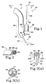
- FIG. 1 is a side elevational view showing a preferred embodiment of the return line assembly, in accordance with the present invention, before connection of the ground probe in the assembly.
- FIG. 2 is a plan view looking along lines 2-2 in FIG. 1 after connection of the ground probe in the assembly.
- FIG. 3(a) is a view partially in section taken along lines 3(a)-3(a) in FIG. 1 revealing details of the tip construction of the signal probe.
- FIG. 3(b) is a sectional view taken along lines 3(b)-3(b) in FIG. 3(a) revealing further details of the tip construction.
- FIG. 4 is similar to FIG. 1 but shows the return line assembly after repositioning of the probes has occurred and further illustrates, in dashed-line view, a high-profile component rising above the measurement plane.
- FIG. 5 is a plan view showing the return line assembly of FIG. 4 as seen by an observer looking down on the assembly after the signal probe has been shifted to the left.
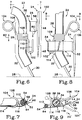
- FIG. 6 is a side elevational view of a second preferred embodiment of the return line assembly before connection of the ground probe in the assembly.
- FIG. 7 is a plan view taken along lines 7-7 in FIG. 6 after connection of the ground probe.
- FIG. 8 is similar to FIG. 6 but shows the assembly after connection of the ground probe and after rotation of a spindle that pulls the strap of the invention against the signal probe.
- FIG. 9 is primarily a plan view taken along lines 9-9 in FIG. 8 where the spindle and ground probes are shown in cut-away and sectional view, respectively, to reveal a connection detail and where alternative positions of these same components are indicated in dashed lines.
- FIGS. 10(a) -10(e) show a preferred process, in accordance with the present invention, for making the sheet-like conductive strap.
- FIG. 10(a) is a transverse sectional view showing the upper portion of a substrate after it has been preheated and after metallic layers have been sputter deposited on the upper portion in accordance with the preferred process.
- FIG. 10(b) shows in sectional view a fragment of the intermediate composite shown in FIG. 10(a) where the fragment has been selected to show how an individual strap is made and where additional photodefining and etching procedures have been carried out in accordance with the preferred process.
- FIG. 10(c) is similar to FIG. 10(b) except showing a subsequent plating procedure in accordance with the preferred process.
- FIG. 10(d) is similar to FIG. 10(c) except showing a subsequent etchback procedure used to form the strap in accordance with the preferred method.
- FIG. 10(e) is a side elevational view illustrating a preferred technique for removing the strap from the substrate, where the position of self-coiling strap is shown just before and just after the start of removal in dashed-line and solid-line view, respectively.
- FIG. 4 shows a preferred embodiment of a return line assembly 20 constructed in accordance with the present invention.
- the assembly includes a signal probe 22 which is electrically connected to a ground probe 24 by a sheet-like conductive strap 25.
- the strap and the ground probe provide a convenient return path for the signal probe so that the signal probe can be returned, for example, to a respective ground site 26a which is set off from the particular measurement site 27a that the signal probe is measuring.
- the ground site 26a and measurement site 27a may be pads or traces that are bonded, for example, to the top surface or measurement plane 28 of a board or wafer, as represented in the drawings by a dashed line.
- the signal and ground probes are mounted from above, each preferably on an X-Y-Z positioner (not shown) of a conventional high-frequency probe station in order to permit multidirectional movement of each probe to other sites.
- the strap 25 includes a self-coiling capability that enhances the electrical and physical operation of the assembly.
- the strap and the operational benefits which its use confers are described following a description of the other components in the return line assembly.
- a second embodiment of the return line assembly is then described followed, finally, by a detailed description of a preferred process for making: the strap.
- the signal probe 22 includes an elongate cylindrical portion 29, a tip portion 30, and a bent end portion 32 that is formed in the signal probe in order to make the tip portion more visible to an observer looking down on the probe.
- the cylindrical portion and bent end portion are formed by semi-rigid cable which is nominally of .047 inch outer diameter.
- the semi-rigid cable is of conventional construction and includes a center conductor 34, inner dielectric 36 and a somewhat stiff but still bendable outer conductive cladding 38.
- the tip portion 30 of the signal probe 22 comprises a microstrip transmission line in which a signal line conductor 40 and a ground line conductor 42 are bonded to the surface of an alumina or other dielectric substrate 43, preferably by a high-definition photolithographic process.
- the signal and ground line conductors are preferably formed of a high conductivity metal, such as gold.
- each line conductor 40 and 42 is plated with a hard metal 44, such as nickel, in order to prevent undue wear.
- a resistive layer 45 is also formed on the substrate in-line with the signal line conductor so that the measurement site is not unduly loaded by the probe.
- an in-line active network can be mounted on the substrate 43 to increase the tip output impedance.
- a portion of the inner dielectric 36 of the semirigid coaxial cable is removed from the bent end portion 32 to create a well 41.
- the well 41 is preferably formed by preheating the semirigid coaxial cable to 240°C for one minute so that the TeflonTM dielectric 36 extrudes out the end of the cable, after which the cable is allowed to cool and the extruded dielectric trimmed off. Physical pressure on the expanded dielectric at the end then suffices to form the well.
- the substrate 43 is then inserted inside the well and the signal and ground line conductors 40 and 42 connected, as shown in FIG. 3(b), to the center conductor 34 and conductive cladding 38 respectively, such as by reflow solder 47.
- This construction provides the signal probe 22 with a controlled impedance along its entire extent despite transformation from a coaxial structure to a microstrip structure.
- the ground probe 24 like the signal probe 22, also has an elongate cylindrical portion 46 and further includes a sharpened needle-like tip 48.
- the ground probe is conventionally formed of a hard conductive metal, and the outer surface 50 of the probe preferably includes a thin plated layer of highly conductive material such as gold.
- the sheet-like conductive strap 25 includes a first end portion 52 and a self-coiling second end portion 54. Except when the second end portion is in its initial or fully-coiled position 55 (FIG. 1), the strap further includes an extended or substantially flat central portion 56 located between the first and second end portions.
- the first end portion 52 of the strap is electrically connected to the conductive cladding 38 of the signal probe by a permanent bonding agent, such as silver epoxy 58, so that an unbreakable or infrangible connection is established between the first end portion and the signal probe 22.
- a permanent bonding agent such as silver epoxy 58
- the automatically detachable connection is preferably made by moving the ground probe 24 toward the strap 25 in the direction-of-attachment 60 that is shown while the second end portion 54 of the strap is in its initial or fully-coiled position 55 so that the sharpened tip 48 of the probe is inserted centrally within the second end portion of the strap.
- This procedure enables electrical connection to be made by probe movement alone.
- FIG. 2 shows how the cylindrical portion 46 of the ground probe rides connectably against the inside coil or turn 64 of the self-coiling second end portion after the tip 48 of the ground probe has been lowered to the same measurement plane 28 as the tip 30 of the signal probe.
- the self-coiling second end portion is now moved to an extended position, that is, to a position in which the strap includes the substantially flat central portion 56.
- the ground line conductor 42 (FIG. 3) of the signal probe is returned or tied to the reference potential of the ground site 26a via the continuous electrical path through the ground probe 24, the strap 25, the silver epoxy 58, and the conductive cladding 38.
- the preferred embodiment 20 of the return line assembly that is shown in FIGS. 1-5 has few parts and that these are easily assembled and is, moreover, readily adaptable to preexisting probe setups since the self-coiling strap 25 can be used without special modification being made to the probes of these other setups.
- the assembly performs well electrically in the sense of having minimal sensitivity to noise.
- the original length 76 of the flat central portion 56 of the strap is automatically reduced to a new second length 78 which is about equal to the spacing between the second measurement site and the ground site. Accordingly, if a noisy component 80 is mounted on the device but is located in a position that is neither near nor between the second measurement site and the ground site, the reduced second length of the central portion affords little opportunity for the noise emitted by this component to electro-magnetically couple into the strap.
- the length 76 of the strap 25 is reduced or increased automatically in accordance with the direction of relative movement between the probes, repositioning of the probes between each individual measurement can be accomplished quickly. This, in turn, shortens the period of time that is needed to test a particular device. For example, referring to FIG. 4, regardless of how far the tip 30 of the signal probe 22 needs to travel in order to move from the first measurement site 27a to the second measurement site 27b, by the time this tip reaches the second measurement site, the original length 76 of the central portion of the strap will have already been reduced correspondingly. This proportional tracking feature is not available, by comparison, in a manual rewind type of interface where larger shifts in probe position translate into more time needed to rewind the excess portion of the strap.
- the component 80 which is represented in dashed lines in FIG. 4, also has a relatively high profile that extends well above the measurement plane 28 of the device. If, for some reason, the tip 30 of the signal probe cannot be moved around the sides of this component in order to reach the second measurement site 27b because, for example, other components are in the way, it is then necessary to use a vertical movement of the signal probe to lift the probe over the component.
- the preferred embodiment 20 allows this vertical movement to occur without also requiring that the ground probe 24 be lifted because the self-coiling second end portion 54 of the strap is slidably movable in the vertical or Z-axis direction 82 across the elongate cylindrical portion 46 of the ground probe while maintaining its connection to the ground probe. Accordingly, there is no need to spend additional time repositioning the tip of the ground probe each time the signal probe is vertically repositioned.
- the station operator attempts to move the signal probe 22 to a third measurement site 27c so that the spacing between the signal and ground probes 22 and 24 now exceeds a predetermined maximum probe distance 86, which is indicated in FIG. 5, the self-coiling second end portion 54 of the strap will automatically detach from the ground probe and resume its initial or fully-coiled position 55 as shown in FIG. 1. This prevents breakage of the ground probe or, alternatively, prevents the sharpened tip 48 of the ground probe from being dragged by the strap across the surface of the device, which action could otherwise scratch or damage the particular surface elements on the device.
- FIGS. 6-9 a second preferred embodiment 100 of the return line assembly is shown. As between FIGS. 6-9 and FIGS. 1-5, like reference numerals have been used to refer to like elements.
- the first end portion 52 of the strap is now connected by silver epoxy 58 to the ground probe 24, rather than to the outer cladding 38 of the signal probe, and the self-coiling second end portion 54 of the strap is now received on a U-shaped post member 102 which is part of a spindle 104 that now engages the signal probe.
- the spindle 104 has three distinct portions including a handle portion 106, a main body portion 108, and the U-shaped post member 102.
- the main body is configured as a series of spirally-wound coils which have an inner diameter suitably dimensioned for frictionally engaging the elongate cylindrical portion 29 of the signal probe.
- the U-shaped post member 102 is attached to the main body so that when the main body is engaged to the signal probe, an inside leg 110 on the post member downwardly extends from the main body toward the probe tip 30, and an opposite outside leg 112 on the post member upwardly extends away from the probe tip back toward the main body. In other words, the post member extends primarily off to one end of the main body as depicted.
- the outside leg 112 of the post member is pin-like in shape in order to facilitate ready insertion of this leg centrally within the respective coils of the second end 54 of the strap when the ground probe 24 is moved along the direction-of-attachment 60.
- the different portions of the spindle 104 are formed by the respective sections of a single piece of stiff conductive wire.
- the self-coiling capability of the strap 25 in the second embodiment minimizes strap length and spurious noise pick-up, enables automatic detachment of the strap when overtravel between the probes occurs, and permits quick probe repositioning between measurements.
- this feature is further enhanced in the second embodiment due to the spindle 104.
- the main body 108 of the spindle only engages the elongate cylindrical portion 29 of the signal probe frictionally, so that it is possible to vary the position of the post member 102 along the vertical axis 82 in a direction either toward or away from the measurement plane 28. Regardless, then, of which probe, signal or ground, is being moved independently vertically, it is possible to keep the strap 25 attached once it is initially connected by making corresponding shifts in the vertical position of the post member.
- the first embodiment 20 as seen most clearly in FIG.
- the spindle 104 is also useful for improving tip visibility during close-in probing. Comparing FIGS. 6 and 8, the frictional engagement between the main body 108 of the spindle and the outer cladding 38 of the signal probe 22 allows the spindle to be rotated by its handle portion 106 about the signal probe. During such rotation, the self-coiling second end portion 54 of the strap is carried toward a far side 114 of the signal probe which is located opposite to that side 116 which faces the ground probe.
- FIGS. 7 and 9, which correspond to FIGS. 6 and 8, show the alternate views that result as seen by an observer who is looking down at the probes before and after, respectively, the spindle has been rotated.
- a low-magnification lens (not shown) is used by the observer to view the setup to ensure that each probe tip is accurately positioned.
- the movement of the self-coiling second end portion 54 to the far side 114 of the signal probe affords the observer a better view (FIG. 9) of the signal probe tip 30 than that view (FIG. 7) which is obtained when the self-coiling second end portion is to the near side 116 of the signal probe, particularly, as shown, during close-in probing where the numerous coils of the second end can completely hide the signal probe tip from view.
- the spindle 104 not only improves tip visibility during close-in probing but also increases, during such probing, the reliability of the electrical interconnection made.
- the outer diameter of the pin-like outside leg 112 of the post member is somewhat smaller than the inside diameter of the inside coil or turn 64 of the second end portion of the strap. While this facilitates initial insertion of the outside leg 112 within the coils of the second end, it also makes it possible for the outside leg to be placed in a position during close-in probing where it does not actually contact the inside turn 64 of the strap.
- the spindle 104 of the second embodiment 100 is rotated during close-in probing to the position shown in solid-view in FIGS. 8 and 9.
- This not only causes the self-coiling second end portion 54 of the strap to be shifted to the far side 114 of the probe, thereby improving visibility, but also causes the central portion 56 of the strap to draw across and bear against the conductive cladding 38 of the probe, thereby establishing a reliable electrical connection 118 with the signal probe.
- the U-shaped post member 102 is off to one end of the main body 108 of the spindle, this connection occurs, as shown in FIG. 8, clear of the main body.
- the self-coiling characteristic of the second end portion 54 keeps the flat central portion 56 of the strap in moderate traction, thereby increasing the connection force.
- the first preferred embodiment 20 of the return line assembly which is shown in FIGS. 1-5
- the second preferred embodiment 100 of the assembly which is shown in FIGS. 6-9
- a preferred process for making the sheet-like strap which takes advantage of thin film technology, is shown in FIGS. 10(a)-10(e).
- the first step in the preferred process is providing a substrate 120 that has an ultrasmooth surface 122 and a relatively low coefficient of thermal expansion (e.g., averaging less than 50 X 10 ⁇ 7/°C over a temperature range of 0°C to 550°C).
- the term "ultrasmooth” is used herein to indicate that the peak-to-valley roughness variations in the surface are a small fraction of the thickness of the thin film layers that are subsequently applied to the surface.
- a suitable material for the substrate is 20 mil thick barium borosilicate glass that has been drawn into sheets of finished thickness and that obtains its smooth final finish directly from the molten glass.
- a commercially available glass of this type is made by Corning Glass Works based in Corning, New York and sold under the manufacturer's designation "Sheet Glass 7059.”
- the glass substrate is preheated on a pallet for a minimum of one hour at 100°C after which it is immediately introduced into the sputtering processing system (not shown) where deposition of succeeding layers occurs.
- additional heat is applied to the glass substrate under a chamber vacuum of below 10 ⁇ 7 torr in order to raise the temperature of the substrate to about 500°C.
- FIG. 10(a) shows a later step in the process, this causes the glass substrate to develop a bowed curvature so that the middle portion 124 of the substrate bulges slightly in a convex direction outwardly away from the end portions 126 of the substrate.
- several layers of alternately different metallic material are deposited on the substrate by sputtering in order to achieve the multilayered intermediate composite 127 depicted in FIG. 10(a).
- sputtering is a process in which a metal target is bombarded with positive ions so that individual atoms of metal are ejected from the target for redeposit on the substrate or other surface desired.
- This process accordingly, can be used to deposit so-called "monolayers" so that metal layers of small but very well-controlled thickness can be made.
- the first layer 128 which is deposited on the substrate is gold (Au) having a thickness within the range of 34A to 48A and preferably of about 42A. The purpose served by the use of such a thin layer is further clarified below.
- the intermolecular forces of adhesion which act along the first interface 130 between the Au layer 128 and the substrate 120 are relatively poor when compared to the normal values that are traditionally sought when creating a thin film bond.
- the traditional object has been to create strong bonds so that the resulting composite will maintain its permanency even when environmental conditions become severe.
- the Au layer 128 adheres only poorly to the glass substrate. This is attributable, on a molecular level, to Au being inert to the oxides in glass.
- a second metallic layer 132 of titanium tungsten (TiW) is next deposited, by sputtering, on the first layer 128 so as to form a second interface 134.
- This alloy is nominally 3% to 20% titanium by weight (preferably 5%), where the remainder is tungsten, and is deposited so that the thickness of the second layer is within the range of 1.0 to 2.5 microns. Within this range, the particular thickness chosen can vary so as to meet the needs of a particular application. For example, to obtain a strap having a large self-coiling bias and a small-diameter inner coil for use with hardened but thin probe tip, a thickness near the upper end of the range is chosen.
- intermolecular forces of adhesion that act along the second interface 134 are relatively large, much larger, for example, than those which act along the first interface 130. This is consistent with the objective of creating a strong permanent bond between the first and second layers.
- intermolecular forces of adhesion also act between the second layer 132 and the substrate 120. That is, they act across the first layer 128. These interlayer forces are attributable, on a molecular level, to the strong metallic bond between the TiW and the gold and the strong chemical bond between the TiW and the oxygen in the glass.
- the last layers which are deposited by the sputtering process are a third layer 136 composed of Au having a nominal thickness of 800A and a fourth layer 138 of TiW which has a composition chemically equivalent to that of the second layer 132 and which has a nominal thickness of 400A.
- the intermediate composite 127 is removed from the sputtering equipment for further processing. The cooling occurring in the substrate after its removal from the heated sputtering chamber further effects the internal compressive forces which act in the deposited metallic layers due to the uneven shrinkage of the substrate and the layers caused by their different coefficients of thermal expansion.
- FIGS. 10(b)-10(d) show, in section, a fragment 139 of the intermediate composite 127 shown in FIG. 10(a) where, for clarity of illustration, the fragment has been selected in order to show additional steps of the preferred process as they relate to forming a single strap.
- the larger piece shown in FIG. 10 will, of course, allow the bulk processing of a number of straps at once, but the process, as it pertains to each strap, is the same. It is further noted here that the dimensional relationships, where they are critical, are specified in the text, and it can in no way be assumed in FIGS. 10(a)-10(e) that each element has been drawn to its correct relative scale.
- the area in which the strap is formed is indicated by reference numeral 140, while the outlying areas are indicated by reference numeral 142.
- a conventional photoresist layer 144 is deposited, preferably by a photolithographic process, on the fourth layer 138 in order to mask the outlying areas 142.
- the TiW layer 138 is etched away from the selected area 140 using a conventional etching agent such as hydrogen peroxide.
- a plating step is performed. Referring to FIG. 10(c), that portion of the Au third layer 136 which is left exposed in the selected area 140 after the etching step is now plated with a fifth layer 146 that is composed of nickel having a thickness within the range of 1.0 to 2.5 microns. Next, the nickel layer is plated with a sixth layer 138 composed of Au and having a thickness within the range of .7 to 1.0 microns.
- the next step in the preferred process of making the strap is to etch away all the material above the substrate 120 which lies outside of the-selected area 140.
- the photoresist layer 144 can be removed with acetone, the outside portions of the first and third layers 128 and 136 of Au can be etched away with potassium iodide, and the outside portions of the second TiW layer 132 can be etched away with hydrogen peroxide.
- the final composite which is left defines a completely formed strap 150.
- the final processing step is to dislodge each completely formed strap 150 from the substrate 120 on which it was made. Desirably this is done before a considerable time has elapsed in order to prevent undue stress relief from occurring in the metallic layers which have been formed.
- the position of the completed strap just before dislodgment is indicated in dashed-line view while a position of the completed strap just after dislodgment is indicated in solid-line view.
- a sharpened edge 152 such as that of a razor blade, is inserted between the first layer 128 (FIG. 10(d)) and the substrate 120 so as to mechanically introduce a position of discontinuity in the first interface 130. If the foregoing steps of the process have each been properly carried out, this has the effect of initiating a self-continuing mechanical reaction or cycle in which the self-coiling bias of the completely formed strap pulls the strap away from the position of discontinuity and thereby produces a second position of discontinuity immediately adjacent to and replacing the first. This reaction sequence successively repeats itself until the position of discontinuity reaches the extreme end 154 of the strap, whereupon the strap is fully released.
- the titanium second layer 132 by means of the strong compressive forces acting in that layer, strips itself and each of the other remaining layers from the substrate, while each of these layers (including the first layer) and all but the first interface are kept intact.
- the first of these relate to the thickness of the first layer 128.
- Minimizing the thickness of the first layer 128 increasingly permits the potentially large forces of adhesion which act between the second layer 132 and the substrate 120 to supplement the relatively weak forces of adhesion which act between the first layer 128 and the substrate.
- the thickness of the first layer not be made too thin or else the self-coiling bias of the strap will not be sufficient to pull the strap away from the substrate.
- the appropriate thickness for the first layer depends on a satisfactory resolution of these competing requirements for the particular choice of material made.
- another set of guidelines can be formulated for choosing the thickness of the second layer 132.
- This thickness, the type of metal used for the layer, and the degree of curvature induced in the surfaces of the substrate 120 by preheating, will cooperatively determine the strength of the compressive forces that act internally in the second layer. For example, if TiW is used in accordance with the preferred process, then the thicker the layer, the greater will be these compressive forces. More generally, when choosing the thickness appropriate for another type of material, the following competing objectives should be kept in mind. On the one hand, the compressive forces which result should not be so high that they cause the completed strap to wrap so tightly on itself that it cannot be penetrated by a probe. On the other hand, these compressive forces should not be so low that they cannot overcome the forces of adhesion which act along the first interface 130. The appropriate thickness for the second layer depends on a satisfactory resolution of these competing requirements for the particular choice of second layer material made.
- another guideline relates to the choice of the substrate 120. If the surface of the substrate is not sufficiently smooth, not only will there be grain displacements and stress disparities in the layers deposited on the substrate, but there will also be interference with the self-releasing behavior described above. In particular, if the substrate surfaces are excessively rough, peaks on the substrate surface will protrude into the first layer 128 (FIG. 10(d)) thereby pinning the first layer to the substrate. Accordingly, a substrate of minimal surface roughness should be chosen.
- a TiW second layer 132 instead of a TiW second layer 132, an Au first layer 128, and a glass substrate 120, it is possible to use many other types of metals (e.g., chromium, vanadium, and tungsten) in the second layer, carbon in the first layer, and alumina in the substrate.
- metals e.g., chromium, vanadium, and tungsten
- the strong metallic bond between the TiW and the gold and the strong chemical bond between the TiW and the oxygen in the glass have their counterpart in the strong metal/carbon bond and the strong metal/oxide bond.
- the return line assembly has now been described, as well as a preferred method of making and connecting the self-coiling strap which is a component of both embodiments, it will be recognized that alternative assemblies and processes are possible without departing from the broader principles of the present invention.
- the first preferred embodiment of the return line assembly it is possible to connect the first end of the strap directly to the ground line conductor on the signal probe tip rather than to the probe's outer cladding.
- the spindle can be configured for mounting on the ground probe instead of the signal probe.
- the method of fabricating the self-coiling strap by using a physical mask during sputter deposition, it is possible to eliminate the photolithographic and etching steps.
Landscapes
- Physics & Mathematics (AREA)
- General Physics & Mathematics (AREA)
- Measuring Leads Or Probes (AREA)
- Testing Of Short-Circuits, Discontinuities, Leakage, Or Incorrect Line Connections (AREA)
Applications Claiming Priority (2)
| Application Number | Priority Date | Filing Date | Title |
|---|---|---|---|
| US07/898,015 US5264788A (en) | 1992-06-12 | 1992-06-12 | Adjustable strap implemented return line for a probe station |
| US898015 | 1992-06-12 |
Publications (2)
| Publication Number | Publication Date |
|---|---|
| EP0578375A2 true EP0578375A2 (de) | 1994-01-12 |
| EP0578375A3 EP0578375A3 (de) | 1995-01-11 |
Family
ID=25408802
Family Applications (1)
| Application Number | Title | Priority Date | Filing Date |
|---|---|---|---|
| EP93304456A Withdrawn EP0578375A3 (de) | 1992-06-12 | 1993-06-08 | Anpassbare band-implementierte Rückleitung für eine Sondenstation. |
Country Status (3)
| Country | Link |
|---|---|
| US (1) | US5264788A (de) |
| EP (1) | EP0578375A3 (de) |
| JP (1) | JPH0650988A (de) |
Cited By (1)
| Publication number | Priority date | Publication date | Assignee | Title |
|---|---|---|---|---|
| EP0953844A3 (de) * | 1998-04-27 | 2001-01-17 | Delaware Capital Formation, Inc. | Zeitbereichsreflektometrie-Prüfanordnung für eine zweidimensinalle Sonde |
Families Citing this family (12)
| Publication number | Priority date | Publication date | Assignee | Title |
|---|---|---|---|---|
| US5446393A (en) * | 1993-05-21 | 1995-08-29 | Schaefer; Richard K. | Electrical measuring and testing probe having a malleable shaft facilitating positioning of a contact pin |
| JPH08233860A (ja) * | 1995-02-28 | 1996-09-13 | Nec Corp | 同軸高周波プローブ及びこの同軸高周波プローブを用いた基板の評価方法 |
| US5994909A (en) * | 1997-08-25 | 1999-11-30 | Lucas; Brian K. | Robotic twin probe for measurement on printed circuit boards and electrical and electronic assemblies |
| EP1141731B1 (de) * | 1998-12-30 | 2003-05-07 | Proteus Corporation | Doppelspitzen-prüftstift zum prüfen von leiterplatten |
| US6798229B2 (en) * | 2000-05-11 | 2004-09-28 | Brian D. Butler | Wide-bandwidth coaxial probe |
| US6965226B2 (en) | 2000-09-05 | 2005-11-15 | Cascade Microtech, Inc. | Chuck for holding a device under test |
| TW200829922A (en) | 2007-01-08 | 2008-07-16 | Microelectonics Technology Inc | High frequency probe |
| US8319503B2 (en) | 2008-11-24 | 2012-11-27 | Cascade Microtech, Inc. | Test apparatus for measuring a characteristic of a device under test |
| US9772391B2 (en) * | 2014-01-24 | 2017-09-26 | Tektronix, Inc. | Method for probe equalization |
| DE102014005339B4 (de) * | 2014-01-28 | 2022-06-09 | Wolfgang B. Thörner | Verfahren zur Herstellung eines Kontaktelements |
| TWI681195B (zh) * | 2018-11-21 | 2020-01-01 | 中華精測科技股份有限公司 | 探針卡裝置及其調節式探針 |
| CN118914617B (zh) * | 2024-08-21 | 2025-02-11 | 江阴佳泰电子科技有限公司 | 用于晶圆级可靠性测试的探针安装结构 |
Family Cites Families (8)
| Publication number | Priority date | Publication date | Assignee | Title |
|---|---|---|---|---|
| CH364040A (fr) * | 1960-04-19 | 1962-08-31 | Ipa Anstalt | Dispositif de détection pour vérifier si un élément d'une installation électrique est sous tension |
| US3256484A (en) * | 1962-09-10 | 1966-06-14 | Tektronix Inc | High voltage test probe containing a part gas, part liquid dielectric fluid under pressure and having a transparent housing section for viewing the presence of the liquid therein |
| DE3125552C1 (de) * | 1981-06-29 | 1982-11-11 | Siemens AG, 1000 Berlin und 8000 München | Prüfeinrichtung zum Anzeigen einer elektrischen Spannung, deren Polarität und zur Durchgangsprüfung |
| CA1154588A (en) * | 1982-02-15 | 1983-10-04 | Robert D. Lamson | Tape measure |
| US4838802A (en) * | 1987-07-08 | 1989-06-13 | Tektronix, Inc. | Low inductance ground lead |
| JPH0616056B2 (ja) * | 1988-01-08 | 1994-03-02 | 株式会社ピーエフユー | 信号測定器の接地用導体構造 |
| US5045781A (en) * | 1989-06-08 | 1991-09-03 | Cascade Microtech, Inc. | High-frequency active probe having replaceable contact needles |
| US4923407A (en) * | 1989-10-02 | 1990-05-08 | Tektronix, Inc. | Adjustable low inductance probe |
-
1992
- 1992-06-12 US US07/898,015 patent/US5264788A/en not_active Expired - Lifetime
-
1993
- 1993-06-08 EP EP93304456A patent/EP0578375A3/de not_active Withdrawn
- 1993-06-10 JP JP5138379A patent/JPH0650988A/ja not_active Withdrawn
Cited By (1)
| Publication number | Priority date | Publication date | Assignee | Title |
|---|---|---|---|---|
| EP0953844A3 (de) * | 1998-04-27 | 2001-01-17 | Delaware Capital Formation, Inc. | Zeitbereichsreflektometrie-Prüfanordnung für eine zweidimensinalle Sonde |
Also Published As
| Publication number | Publication date |
|---|---|
| JPH0650988A (ja) | 1994-02-25 |
| US5264788A (en) | 1993-11-23 |
| EP0578375A3 (de) | 1995-01-11 |
Similar Documents
| Publication | Publication Date | Title |
|---|---|---|
| US5264788A (en) | Adjustable strap implemented return line for a probe station | |
| EP0925803B1 (de) | Führungsdraht | |
| US6118287A (en) | Probe tip structure | |
| US7548082B2 (en) | Inspection probe | |
| US6684499B2 (en) | Method for fabricating a spring structure | |
| EP1277696B1 (de) | Feder mit leitfähiger Beschichtung | |
| JP3135930B2 (ja) | 薄膜電気装置 | |
| JP4560221B2 (ja) | コンタクトストラクチャとその製造方法 | |
| US7985081B2 (en) | Transferable micro spring structure | |
| JPH0451535A (ja) | 半導体lsi検査装置用プローブヘッドの製造方法および検査装置 | |
| US20050136562A1 (en) | Membrane probing system | |
| US20060061348A1 (en) | High frequency oscilloscope probe with unitized probe tips | |
| KR100819258B1 (ko) | 프로브 구조물 및 이의 제조 방법 | |
| EP0617916B1 (de) | Sonde mit mehreren Elektroden und Herstellungsverfahren | |
| WO2005072438A2 (en) | Multi-signal single beam probe | |
| US5903161A (en) | Electrically conductive rod-shaped single crystal product and assembly for measuring electrical properties employing such product, as well as processes for their production | |
| US20240085454A1 (en) | Coaxial wafer probe and corresponding manufacturing method | |
| US20190385969A1 (en) | Coaxial wire | |
| JPH1144708A (ja) | コンタクトプローブおよびその製造方法 | |
| US4613404A (en) | Materials which exhibit a surface active effect with vacuum baked photoresists and method of using the same | |
| EP0632487B1 (de) | Verfahren zur Herstellung eines Siliziumkörper enthaltenden Gegenstands | |
| Yang et al. | rf‐diode sputtered Permalloy film | |
| JP3156874B2 (ja) | 回路測定用端子およびその製造方法 | |
| JP3423498B2 (ja) | Emc用近磁界プローブ及びその作製方法 | |
| JP3058514B2 (ja) | 金属箔を加工した探針部品の製造方法 |
Legal Events
| Date | Code | Title | Description |
|---|---|---|---|
| PUAI | Public reference made under article 153(3) epc to a published international application that has entered the european phase |
Free format text: ORIGINAL CODE: 0009012 |
|
| AK | Designated contracting states |
Kind code of ref document: A2 Designated state(s): AT BE CH DE DK ES FR GB GR IE IT LI LU MC NL PT SE |
|
| PUAL | Search report despatched |
Free format text: ORIGINAL CODE: 0009013 |
|
| AK | Designated contracting states |
Kind code of ref document: A3 Designated state(s): AT BE CH DE DK ES FR GB GR IE IT LI LU MC NL PT SE |
|
| STAA | Information on the status of an ep patent application or granted ep patent |
Free format text: STATUS: THE APPLICATION IS DEEMED TO BE WITHDRAWN |
|
| 18D | Application deemed to be withdrawn |
Effective date: 19950712 |