EP0574025A2 - Optiches Aufzeichungsmedium und Verfahren zur Herstellung desselben - Google Patents
Optiches Aufzeichungsmedium und Verfahren zur Herstellung desselben Download PDFInfo
- Publication number
- EP0574025A2 EP0574025A2 EP19930109470 EP93109470A EP0574025A2 EP 0574025 A2 EP0574025 A2 EP 0574025A2 EP 19930109470 EP19930109470 EP 19930109470 EP 93109470 A EP93109470 A EP 93109470A EP 0574025 A2 EP0574025 A2 EP 0574025A2
- Authority
- EP
- European Patent Office
- Prior art keywords
- layer
- recording
- dielectric
- recording layer
- recording medium
- Prior art date
- Legal status (The legal status is an assumption and is not a legal conclusion. Google has not performed a legal analysis and makes no representation as to the accuracy of the status listed.)
- Granted
Links
Images

Classifications
-
- G—PHYSICS
- G11—INFORMATION STORAGE
- G11B—INFORMATION STORAGE BASED ON RELATIVE MOVEMENT BETWEEN RECORD CARRIER AND TRANSDUCER
- G11B7/00—Recording or reproducing by optical means, e.g. recording using a thermal beam of optical radiation by modifying optical properties or the physical structure, reproducing using an optical beam at lower power by sensing optical properties; Record carriers therefor
- G11B7/24—Record carriers characterised by shape, structure or physical properties, or by the selection of the material
- G11B7/241—Record carriers characterised by shape, structure or physical properties, or by the selection of the material characterised by the selection of the material
- G11B7/242—Record carriers characterised by shape, structure or physical properties, or by the selection of the material characterised by the selection of the material of recording layers
- G11B7/243—Record carriers characterised by shape, structure or physical properties, or by the selection of the material characterised by the selection of the material of recording layers comprising inorganic materials only, e.g. ablative layers
- G11B2007/24302—Metals or metalloids
- G11B2007/24306—Metals or metalloids transition metal elements of groups 3-10
-
- G—PHYSICS
- G11—INFORMATION STORAGE
- G11B—INFORMATION STORAGE BASED ON RELATIVE MOVEMENT BETWEEN RECORD CARRIER AND TRANSDUCER
- G11B7/00—Recording or reproducing by optical means, e.g. recording using a thermal beam of optical radiation by modifying optical properties or the physical structure, reproducing using an optical beam at lower power by sensing optical properties; Record carriers therefor
- G11B7/24—Record carriers characterised by shape, structure or physical properties, or by the selection of the material
- G11B7/241—Record carriers characterised by shape, structure or physical properties, or by the selection of the material characterised by the selection of the material
- G11B7/242—Record carriers characterised by shape, structure or physical properties, or by the selection of the material characterised by the selection of the material of recording layers
- G11B7/243—Record carriers characterised by shape, structure or physical properties, or by the selection of the material characterised by the selection of the material of recording layers comprising inorganic materials only, e.g. ablative layers
- G11B2007/24302—Metals or metalloids
- G11B2007/24308—Metals or metalloids transition metal elements of group 11 (Cu, Ag, Au)
-
- G—PHYSICS
- G11—INFORMATION STORAGE
- G11B—INFORMATION STORAGE BASED ON RELATIVE MOVEMENT BETWEEN RECORD CARRIER AND TRANSDUCER
- G11B7/00—Recording or reproducing by optical means, e.g. recording using a thermal beam of optical radiation by modifying optical properties or the physical structure, reproducing using an optical beam at lower power by sensing optical properties; Record carriers therefor
- G11B7/24—Record carriers characterised by shape, structure or physical properties, or by the selection of the material
- G11B7/241—Record carriers characterised by shape, structure or physical properties, or by the selection of the material characterised by the selection of the material
- G11B7/242—Record carriers characterised by shape, structure or physical properties, or by the selection of the material characterised by the selection of the material of recording layers
- G11B7/243—Record carriers characterised by shape, structure or physical properties, or by the selection of the material characterised by the selection of the material of recording layers comprising inorganic materials only, e.g. ablative layers
- G11B2007/24302—Metals or metalloids
- G11B2007/2431—Metals or metalloids group 13 elements (B, Al, Ga, In)
-
- G—PHYSICS
- G11—INFORMATION STORAGE
- G11B—INFORMATION STORAGE BASED ON RELATIVE MOVEMENT BETWEEN RECORD CARRIER AND TRANSDUCER
- G11B7/00—Recording or reproducing by optical means, e.g. recording using a thermal beam of optical radiation by modifying optical properties or the physical structure, reproducing using an optical beam at lower power by sensing optical properties; Record carriers therefor
- G11B7/24—Record carriers characterised by shape, structure or physical properties, or by the selection of the material
- G11B7/241—Record carriers characterised by shape, structure or physical properties, or by the selection of the material characterised by the selection of the material
- G11B7/242—Record carriers characterised by shape, structure or physical properties, or by the selection of the material characterised by the selection of the material of recording layers
- G11B7/243—Record carriers characterised by shape, structure or physical properties, or by the selection of the material characterised by the selection of the material of recording layers comprising inorganic materials only, e.g. ablative layers
- G11B2007/24302—Metals or metalloids
- G11B2007/24314—Metals or metalloids group 15 elements (e.g. Sb, Bi)
-
- G—PHYSICS
- G11—INFORMATION STORAGE
- G11B—INFORMATION STORAGE BASED ON RELATIVE MOVEMENT BETWEEN RECORD CARRIER AND TRANSDUCER
- G11B7/00—Recording or reproducing by optical means, e.g. recording using a thermal beam of optical radiation by modifying optical properties or the physical structure, reproducing using an optical beam at lower power by sensing optical properties; Record carriers therefor
- G11B7/24—Record carriers characterised by shape, structure or physical properties, or by the selection of the material
- G11B7/241—Record carriers characterised by shape, structure or physical properties, or by the selection of the material characterised by the selection of the material
- G11B7/242—Record carriers characterised by shape, structure or physical properties, or by the selection of the material characterised by the selection of the material of recording layers
- G11B7/243—Record carriers characterised by shape, structure or physical properties, or by the selection of the material characterised by the selection of the material of recording layers comprising inorganic materials only, e.g. ablative layers
- G11B2007/24302—Metals or metalloids
- G11B2007/24316—Metals or metalloids group 16 elements (i.e. chalcogenides, Se, Te)
-
- G—PHYSICS
- G11—INFORMATION STORAGE
- G11B—INFORMATION STORAGE BASED ON RELATIVE MOVEMENT BETWEEN RECORD CARRIER AND TRANSDUCER
- G11B7/00—Recording or reproducing by optical means, e.g. recording using a thermal beam of optical radiation by modifying optical properties or the physical structure, reproducing using an optical beam at lower power by sensing optical properties; Record carriers therefor
- G11B7/24—Record carriers characterised by shape, structure or physical properties, or by the selection of the material
- G11B7/241—Record carriers characterised by shape, structure or physical properties, or by the selection of the material characterised by the selection of the material
- G11B7/252—Record carriers characterised by shape, structure or physical properties, or by the selection of the material characterised by the selection of the material of layers other than recording layers
- G11B7/254—Record carriers characterised by shape, structure or physical properties, or by the selection of the material characterised by the selection of the material of layers other than recording layers of protective topcoat layers
- G11B7/2542—Record carriers characterised by shape, structure or physical properties, or by the selection of the material characterised by the selection of the material of layers other than recording layers of protective topcoat layers consisting essentially of organic resins
-
- G—PHYSICS
- G11—INFORMATION STORAGE
- G11B—INFORMATION STORAGE BASED ON RELATIVE MOVEMENT BETWEEN RECORD CARRIER AND TRANSDUCER
- G11B7/00—Recording or reproducing by optical means, e.g. recording using a thermal beam of optical radiation by modifying optical properties or the physical structure, reproducing using an optical beam at lower power by sensing optical properties; Record carriers therefor
- G11B7/24—Record carriers characterised by shape, structure or physical properties, or by the selection of the material
- G11B7/241—Record carriers characterised by shape, structure or physical properties, or by the selection of the material characterised by the selection of the material
- G11B7/252—Record carriers characterised by shape, structure or physical properties, or by the selection of the material characterised by the selection of the material of layers other than recording layers
- G11B7/257—Record carriers characterised by shape, structure or physical properties, or by the selection of the material characterised by the selection of the material of layers other than recording layers of layers having properties involved in recording or reproduction, e.g. optical interference layers or sensitising layers or dielectric layers, which are protecting the recording layers
-
- G—PHYSICS
- G11—INFORMATION STORAGE
- G11B—INFORMATION STORAGE BASED ON RELATIVE MOVEMENT BETWEEN RECORD CARRIER AND TRANSDUCER
- G11B7/00—Recording or reproducing by optical means, e.g. recording using a thermal beam of optical radiation by modifying optical properties or the physical structure, reproducing using an optical beam at lower power by sensing optical properties; Record carriers therefor
- G11B7/24—Record carriers characterised by shape, structure or physical properties, or by the selection of the material
- G11B7/241—Record carriers characterised by shape, structure or physical properties, or by the selection of the material characterised by the selection of the material
- G11B7/252—Record carriers characterised by shape, structure or physical properties, or by the selection of the material characterised by the selection of the material of layers other than recording layers
- G11B7/258—Record carriers characterised by shape, structure or physical properties, or by the selection of the material characterised by the selection of the material of layers other than recording layers of reflective layers
-
- Y—GENERAL TAGGING OF NEW TECHNOLOGICAL DEVELOPMENTS; GENERAL TAGGING OF CROSS-SECTIONAL TECHNOLOGIES SPANNING OVER SEVERAL SECTIONS OF THE IPC; TECHNICAL SUBJECTS COVERED BY FORMER USPC CROSS-REFERENCE ART COLLECTIONS [XRACs] AND DIGESTS
- Y10—TECHNICAL SUBJECTS COVERED BY FORMER USPC
- Y10S—TECHNICAL SUBJECTS COVERED BY FORMER USPC CROSS-REFERENCE ART COLLECTIONS [XRACs] AND DIGESTS
- Y10S428/00—Stock material or miscellaneous articles
- Y10S428/913—Material designed to be responsive to temperature, light, moisture
-
- Y—GENERAL TAGGING OF NEW TECHNOLOGICAL DEVELOPMENTS; GENERAL TAGGING OF CROSS-SECTIONAL TECHNOLOGIES SPANNING OVER SEVERAL SECTIONS OF THE IPC; TECHNICAL SUBJECTS COVERED BY FORMER USPC CROSS-REFERENCE ART COLLECTIONS [XRACs] AND DIGESTS
- Y10—TECHNICAL SUBJECTS COVERED BY FORMER USPC
- Y10S—TECHNICAL SUBJECTS COVERED BY FORMER USPC CROSS-REFERENCE ART COLLECTIONS [XRACs] AND DIGESTS
- Y10S430/00—Radiation imagery chemistry: process, composition, or product thereof
- Y10S430/146—Laser beam
-
- Y—GENERAL TAGGING OF NEW TECHNOLOGICAL DEVELOPMENTS; GENERAL TAGGING OF CROSS-SECTIONAL TECHNOLOGIES SPANNING OVER SEVERAL SECTIONS OF THE IPC; TECHNICAL SUBJECTS COVERED BY FORMER USPC CROSS-REFERENCE ART COLLECTIONS [XRACs] AND DIGESTS
- Y10—TECHNICAL SUBJECTS COVERED BY FORMER USPC
- Y10T—TECHNICAL SUBJECTS COVERED BY FORMER US CLASSIFICATION
- Y10T428/00—Stock material or miscellaneous articles
- Y10T428/31504—Composite [nonstructural laminate]
- Y10T428/31678—Of metal
Definitions
- This invention relates to an optical recording medium applied to record and erase information by use of a recording layer changing its crystallographic state, and a method for preparing the same.
- phase change type wherein laser light is directed to the recording layer to change its crystallographic phase whereby a change of reflectivity with such a crystallographic transition is detected.
- Optical recording media with the phase change materials have been gradually attractive because of not only the capability of a single beam overwriting, but also a relatively simple optical system as compared with magneto-optical recording system.
- Ge-Te or Ge-Te-Sb have been widely used as the phase change materials, because of providing a wide reflectivity change between the crystalline and amorphous states and the materials show good durability. It has been recently proposed to use new compounds known as chalcopyrites. Chalcopyrite type compounds have been investigated as compound semiconductor materials for years and have been applied to solar batteries and so on. The chalcopyrite type compounds are composed of Ib-IIIb-VIb2 or IIb-IVb-Vb2 of the Periodic Table and the compounds have two stacked diamond structures. The basic characteristics are well described, for example, in "Physics", Vol. 8, No. 8 (1987), pp. 441 and Electrochemistry, Vol. 56, No. 4 (1988), pp. 228.
- JP-A 240590/1991 discloses an information recording medium having a recording layer predominantly comprising (AgInTe2) 1-a M a wherein M is Sb and/or Bi and 0.30 ⁇ a ⁇ 0.92 and having a mixture of AgInTe2 and M phases.
- the alleged advantages include improvements in laser writing sensitivity, complete erasability, overwriting properties and the erasing ratio.
- Optical recording disks which can be recorded and reproduced especially at the same linear velocity (1.2 to 1.4 m/s) of the present compact disk (CD) have been greatly interested because of sharing the same drive unit of the present CD by adjusting or modifying the optical system.
- Write-once disks of this type have been developed by use of an organic dyes film as the recording material.
- rewritable one has not been proposed nor developed yet.
- the above-mentioned optical recording disks with the optical phase change have been expected well for this application because of its good erasability and unnecessity of a complicated drive system like magneto-optical system.
- Example of JP-A 240590/1991 referred to above signals were recorded, while rotating the disk at a linear velocity of 7 m/s.
- C/N ratio dropped so rapidly and showed poor repetition of overwriting in comparison with the obtained properties at 7.0 m/s.
- the film composition claimed in the above-mentioned application shows superb properties on recording and erasability at 7.0 m/s, however, the crystallization time of the film does not fit to the recording at a linear velocity of 1.4 m/s, because the crystallization time mostly depends on the alloy composition. Also the crystallization time relies on the disk structure. It is necessary to apply so called "a rapidly cooling strucutre", to solidify the amorphous state after the melting by the incident laser power.
- an object of the present invention is to provide a novel and improved optical recording medium of the phase change type having a recording layer of a (Ag,Au)In(Te,Se)2(Sb,Bi) system belonging to the chalcopyrite type wherein the crystallization time or speed of the recording layer is slowered, thereby improving C/N and repetitive recording capability upon movement of the recording layer relative to a light beam at a relatively low speed around 1.2 to 1.4 m/s.
- Another object of the present invention is to provide a novel and improved optical recording medium of the phase change type capable of reproduction compatible with the CD standard.
- the present invention provides an optical recording medium comprising a recording layer on a substrate wherein information is recorded and erased by exposing the recording layer to a light beam for causing the recording layer to change its crystallographic state.
- the recording layer comprises a recording material containing, preferably consisting essentially of A, B, C, MI, and MII wherein A is at least one of silver and gold, B is indium, C is at least one of tellurium and selenium, MI is at least one of antimony and bismuth, and MII is at least one element selected from the group consisting of titanium, zirconium, hafnium, vanadium, niobium, tantalum, manganese, tungsten and molybdenum, the atomic ratio of the respective elements in the recording material being represented by the formula: [(A a B b C 1-a-b ) x MI 1-x ] 1-y MII y wherein letters a, b, x and y are in the ranges: 0.01 ⁇ a
- the optical recording medium has on the substrate, a lower dielectric layer, the recording layer, an upper dielectric layer, a reflective layer, and a protective layer in the described order.
- the lower dielectric layer includes at least one laminate consisting of two dielectric laminae having different refractive index.
- the dielectric lamina having a higher refractive index in the laminate is disposed adjacent to the substrate.
- one dielectric lamina has refractive index of at least 2 and the other dielectric lamina has a refractive index of less than 2 as measured over a light wavelength of 400 to 850 nm.
- the upper dielectric layer has a refractive index of at least 2 as measured at a wavelength of 400 to 850 nm.
- the recording layer further contains a dielectric material which has a refractive index of at least 1.4 as measured over a light wavelength of 400 to 850 nm.
- the recording material is at least 50% by volume of the recording material and the rest is the dielectric material combined.
- the recording layer can be formed on a substrate by a multiple source sputtering technique using a target of the recording material and a target of the dielectric material, while rotating the substrate at a rotational speed of 1 to 10 rpm relative to the respective targets.
- the crystallization speed or time of a (Ag,Au)In(Te,Se)2-(Sb,Bi) system composition is substantially reduced by adding MII thereto.
- the present invention when applied to optical recording disks to be operated at a relatively low linear velocity around 1.2 to 1.4 m/s, achieves satisfactory C/N and improves repetitive recording capability, especially one beam direct overwriting cpability.
- the recording layer is formed of a mixture of a recording material and a dielectric material
- modulation is substantially improved since the reflectivity of amorphous state and the ratio of the reflectivity of the crystalline state and that of the armorphous is substantially lowered. This is because the recording layer mixed with dielectric material can decrease light absorption coefficient even when the layer is a few times thicker than that of the recording material itself.
- the recording material has a real part of a refractive index n of from about 4 to about 6 (4 in amorphous state and 6 in crystalline state) and the imaginary part of the index k of from about 2.2 to about 3.3 (2.2 in amorphous state and 3.3 in crystalline state) while the dielectric material has a relatively lower refractive index n of about 1.4 to about 2.7.
- the imaginary part of the index k drastically or exponentially decreases when the mixing ratio of dielectric material to the recording material is increased though the real part of refractive index n monotonieally decreases thereo, resulting in the recording layer having a considerably decreased percent light absorption per unit thickness. This property is very applicable to enhance the phase difference effect of reflected light, resulting in the reflectivity difference between the crystalline or microcrystalline and amorphous states. Consequently, the modulation becomes larger.
- the optical recording medium of the invention generally has on the substrate, a lower dielectric layer, a recording layer, an upper dielectric layer, a reflective layer, and a protective resin layer in the described order.
- the lower dielectric layer includes a laminate of a high refractive index of lamina and a lower refractive index lamina, in this case, the reflectivity is superb, or greatly improved to accommodate for standard CD reproduction.
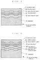
- FIG. 1 is a fragmental cross-sectional view of an optical recording medium according to one preferred embodiment of the invention.
- FIG. 2 is a fragmental cross-sectional view of an optical recording medium according to another preferred embodiment of the invention.
- FIG. 3 is a STM photomicrograph of the surface of the recording layer formed in Example 1 showing a crystalline structure.
- the optical recording medium of the invention is of the type comprising a recording layer on a substrate wherein information is recorded and erased by radiating the recording layer by a light beam for causing a recording material in the recording layer to change between its two crystallographic states, reversively.
- the recording material of which the recording layer is made contains A, B, C, MI, and MII wherein A is silver and/or gold, B is indium, C is tellurium and/or selenium, MI is antimony and/or bismuth, and MII is at least one element selected from the group consisting of titanium, zirconium, hafnium, vanadium, niobium, tantalum, manganese, tungsten and molybdenum.
- the atomic ratio of the respective elements in the recording material is represented by the formula: [(A a B b C 1-a-b ) x MI 1-x ] 1-y MII y wherein letters a, b, x and y are in the ranges: 0.01 ⁇ a ⁇ 0.50, preferably 0.20 ⁇ a ⁇ 0.40, 0.01 ⁇ b ⁇ 0.50, preferably 0.03 ⁇ b ⁇ 0.20, 0.30 ⁇ x ⁇ 0.70, preferably 0.40 ⁇ x ⁇ 0.60, and 0.001 ⁇ y ⁇ 0.20, preferably 0.001 ⁇ y ⁇ 0.01.
- Elements A, B and C are preferably contained in the stoichiometric composition of chalcopyrite type compounds, that is, in the proportion of ABC2, but may deviate therefrom as represented by A a B b C 1-a-b in the above formula.
- the phase change produces an insufficient change of reflectivity.
- the crystal transition rate or the crystallization speed or time becomes so high that no satisfactory C/N would be achieved at a low linear velocity of about 1.2 to 2.8 m/s.
- the phase change cannot make a sufficient reflectivity difference, either.
- the crystallization speed or time becomes so high that no satisfactory C/N would be achieved when long time signals such as 11T signals are recorded at a low linear velocity and the repetitive recording times is decreased.
- y is beyond the above-defined range, recording characteristics become too poor to obtain a sufficient contrast of signals.
- titanium and vanadium, especially Ti is more effective for reducing the crystallization speed or time.
- vanadium and titanium, especially V are more effective. Accordingly, it is preferred that at least one of titanium and vanadium, especially V occupy at least 80 at%, especially 100 at% of the total of MII elements.
- the proportion of antimony and bismuth as MI elements is not critical.
- the recording layer may further contain a trace amount of impurities such as Cu, Ni, Zn, Fe, O, N and C, preferably in a total amount of 0.05 at% or less.
- the recording layer contains not only the recording material, but also a dielectric material.
- the dielectric material contained in the recording layer is not critical and may be selected from various transparent ceramics including silicon oxide such as SiO2, silicon nitride such as Si3N4, zinc sulfide such as ZnS, and mixtures thereof, and various species of glass. Also useful are so-called LaSiON materials containing La, Si, O and N, so-called SiAlON materials containing Si, Al, O and N, and yttrium-containing SiAlON materials.
- Preferred dielectric materials have a refractive index of at least 1.4, especially at least 2 over the wavelength range of 400 to 850 nm.
- This wavelength range includes 780 nm which is the wavelength normally used in current CD players and represents the range over which the optical recording medium of the invention is advantageously operated for writing.
- Preferred examples of the dielectric material are a mixture of ZnS and SiO2, a mixture of ZnS and Si3N4, and a mixture of ZnS and Ta2O5.
- the recording layer contains the recording material and the dielectric material such that the recording material is at least 50% by volume, especially 60 to 80% by volume of the recording material and the dielectric material combined.
- the proportion of the recording material is too high, the absorption coefficient becomes high, that is, high reflectivity from the disk is not obtained because of the less interference effect. Therefore high modulation is not performed between the ceystalline and armorphous states.
- the proportion of the recording material is less than 50% by volume, the absorption coefficient of the recording layer becomes low and the linkage of the crystalline phase clusters is not mature. That is, the opticla phase change can not happen well.
- the recording layer may have any desired thickness although a thickness of about 100 to 2,000 ⁇ , especially about 150 to 1,500 ⁇ is preferred for reflectivity and modulation.
- the recording layer may be formed by any desired method, for example, sputtering and evaporation.
- a recording layer containing both a recording material and a dielectric material is preferably formed by a multiple source sputtering technique using a plurality of targets, typically a target of recording material and a target of dielectric material. With these targets set to face a substrate, sputtering is carried out while rotating the substrate relative to the targets.
- the rotational speed of the substrate relative to the targets preferably ranges from 1 to 10 rpm. A slower speed would fail to achieve uniform dispersion of both the materials in the layer whereas a faster speed would provide a high degree of dispersion to inhibit crystal growth and the linkage upon crystallization.
- a composite target containing both recording and dielectric materials may also be used.
- the recording layer formed by sputtering is generally believed as having a structure wherein particles of the dielectric material are dispersed in the recording material.
- the optical recording medium 1 has a lower dielectric layer 3, a recording layer 4, an upper dielectric layer 5, a reflective layer 6, and a protective layer 7 on a substrate 2.
- the substrate 2 is preferably formed of a material substantially transparent to such a light beam, for example, resins and glass.
- resins are preferred substrate materials.
- a choice may be made among various resins such as acrylic resins, polycarbonate, epoxy resins and polyolefins.
- the shape and dimensions of the substrate are not critical although it is generally of disk shape having a diameter of about 50 to 360 mm and a thickness of about 0.5 to 3 mm.
- the substrate surface may be provided with a predetermined pattern of grooves for tracking and addressing purposes.
- the dielectric layers play the role of protecting the recording layer and confine the thermal expansion of the melting state when a light beam is irradiated, and quickly release the heat to a meltal reflector in order to solidify the amorphous state.
- the lower and upper dielectric layers 3 and 5 are made of any desired dielectric material, for example, selected from those exemplified for the dielectric material contained in the recording layer, preferably those having a relatively high refractive index.
- the lower dielectric layer 3 is about 500 to 3,000 ⁇ thick and the upper dielectric layer 5 is about 100 to 500 ⁇ or about 800 to 2,000 ⁇ thick. Higher modulation is available with these thickness ranges at light wavelength of 700-850 nm.
- the recording layer becomes of the so-called rapid cooling structure that the cooling rate upon recording is designed to be the highest, ensuring formation of recorded marks having a clear shape with low jitter.
- the recording layer becomes of the so-called gradual cooling structure that the cooling rate upon recording is relatively lower than that of rapid cooling structure.
- This structure has an advantage to record and erase with lower laser power, however, disadvantage for repetition times and relatively smaller modulation.
- the dielectric layers are preferably formed by gas phase growth methods such as sputtering and evaporation.
- the reflective layer 6 may be formed of any desired material, typically high reflectivity metals, for example, Al, Au, Ag, Pt, and Cu alone or alloys containing at least one of these metals.
- the reflective layer is preferably about 300 to 1,500 ⁇ thick. Total reflectivity back through the substrate with the layers above would be lower by transmission through the reflective layer if the thickness is thinner than the range. A thickness beyond this range would provide no additional improvement in reflectivity and increase the production cost.
- the reflective layer is preferably formed by gas phase growth methods such as sputtering and evaporation.
- the protective layer 7 is provided for improving scratch resistance and corrosion resistance.
- the protective layer is formed of organic materials, typically radiation curable compounds or compositions which are cured with radiation such as electron and UV radiation.
- the protective layer is generally about 0.1 to 100 ⁇ m thick and may be formed by conventional techniques such as spin coating, gravure coating, spray coating, and dipping.
- the lower dielectric layer includes at least one laminate consisting of two dielectric laminae having different refractive indices.
- the dielectric lamina having a higher refracive index in the laminate is disposed adjacent to the substrate.
- FIG. 2 shows one preferred configuration for this embodiment.
- the optical recording medium 1 is shown as having a dielectric layer with a higher refractive index 31, a dielectric layer with a lower refractive index 32, a recording layer 4, an upper dielectric layer 5, a reflective layer 6, and a protective layer 7 on a substrate 2.
- the high refractive index dielectric layer 31 and a lower refractive index dielectric layer 32 constitutes the laminate.
- the dielectric material of which the high refractive index layer 31 is made should preferably have a relatively higher refractive index like the dielectric material to be contained in the recording layer, typically the index of at least 2 as measured at a wavelength of 400 to 850 nm.
- the dielectric material of which the low refractive index layer 32 is made should preferably have a relatively lower refractive index, typically the index of less than 2 as measured at a wavelength of 400 to 850 nm.
- Useful dielectric materials include SiO2, MgF2, CaF2, LiF2 and mixtures thereof. It will be understood that reflectivity is further improved by providing more than one such laminate. In practice, however, one or two laminates are preferred because a larger number of laminates reduce modulation. Also it may be possible to make a dielectric layer with ⁇ /2 optical thickness on the laminate because of no effect on the intereference.
- the high refractive index layer 31 is about 500 to 1,500 ⁇ thick and the low refractive index layer 32 is about 300 to 1,500 ⁇ .
- the laminate on the substrate side includes a high refractive index layer of about 750 to 900 ⁇ thick, more preferably 800 to 850 ⁇ thick and a low refraction index layer of about 400 to 500 ⁇ thick
- the other laminate on the recording layer side includes a high refractive index layer of about 750 to 900 ⁇ thick, more preferably 800 to 850 ⁇ thick and a low refractive index layer of about 1,000 to 1,400 ⁇ thick, more preferably 1,200 to 1,300 ⁇ thick.
- the substrate 2, recording layer 4, upper dielectric layer 5, reflective layer 6 and protective layer 7 are the same as those of FIG. 1. As mentioned above, it may be possible to make on the dielectric layer a high refractive index layer with a ⁇ /2 optical thickness because this layer has no role for optical interference.
- the recording layer is preferably about 150 to 500 ⁇ thick when formed solely of a recording material and about 200 to 1,000 ⁇ thick when formed of a mixture of recording and dielectric materials.
- the upper dielectric layer is formed of a dielectric material having a relatively high refractive index of at least 2.
- the recording layer has crystallized over the entire area in an initialized state.
- a recording light beam typically laser beam is directed to the recording layer in crystalline state and is focused on the surface. Then the recording material is melted within the irradiated spot. After removal of the recording light beam, the temperature of the spot decreases quickly so that the molten spot is subsequently solidified to amorphous or microcrystalline to form a signal recorded mark.
- the optical recording medium of the present invention ensures high contrasted reflectivity change between the signal recorded marks and the other area and high C/N even when the rotational speed of the recording layer relative to the recording light beam is low and the cooling rate of the irradiated spot is relatively low.
- a recording light beam is directed to a spot of the recording layer where a signal is to be newly written while an erasing light beam is continuously directed to the remaining spots.
- the spots where the erasing light beam is irradiated are heated, however, the temperature is relatively low and below the melting point of the recording material because the erasing light beam is set to relatively low power as compared with the recording light beam in order not to melt the material.
- the resultant heat accumulation provides a gradual temperature cooling so that the cooling rate of the layer is slower than the crystallization time or speed, allowing for crystallization.
- the spot When the recording spot is once melted upon exposure to the recording light beam, the spot remains in the amorphous or microcrystalline state because the heat is quickly diffused toward the reflective layer through an upper dielectric layer to solidity the amorphous mark. Accordingly, upon rewriting, whether the recording material is crystalline or amorphous (or microcrystalline) before irradiation, those portions irradiated with the recording light beam all become amorphous (or microcrystalline) and those portions irradiated with the erasing light beam all become crystalline. Simple overwrite recording is done in this way. However, such overwrite recording can be carried out by using one single light beam which is modulated into recording and erasing light beam power.
- the recording light beam is emitted in pulses.
- the heat accumulation at the recording spot is dispersed quickly in the separated time interval.
- a teardrop shape mark which decreases C/N and increases jitter, is greatly improved by this effect.
- the pulse irradiation also provides an increase of erasing rate.
- the power Pw of the recording light beam and the power Pe of the erasing light beam may be empirically determined.
- Preferred ranges of Pw and Pe are as follows. In the configuration of FIG. 1 wherein the recording layer is formed of a recording material alone or a mixture of recording and dielectric materials, Pw is at least 12 mW and Pe is 4 to 7 mW for the upper dielectric layer which is thin and of the rapid cooling system, type and Pw is 8 to 14 mW and Pe is 2 to 4 mW for the upper dielectric layer which is thick and of the gradual cooling system.
- Pw is at least 12 mW and Pe is 4 to 7 mW for the upper dielectric layer which is thin and of the rapid cooling system
- type and Pw is 8 to 14 mW and Pe is 2 to 4 mW for the upper dielectric layer which is thick and of the gradual cooling system.
- the recording layer is formed of a recording material alone
- Pw is at least 30 mW and Pe is 18 to 25 mW for the upper dielectric layer of the rapid cooling system and Pw is 15 to 20 mW and Pe is 8 to 10 mW for the upper dielectric layer of the gradual cooling system.
- Pw is at least 30 mW and Pe is at least 20 mW for the upper dielectric layer of the rapid cooling system and Pw is 12 to 18 mW and Pe is 6 to 10 mW for the upper dielectric layer of the gradual cooling system.
- the reproducing light beam should be of a low power which does not affect the crystallographic state of the recording layer. Understandably the signal recorded portions in amorphous or microcrystalline state give lower reflectivity than the unrecorded portions in crystalline state.
- the optical recording medium of the invention is operated by rotating it to provide a relative speed of the recording layer relative to the respective light beams of about 1.2 to 2.8 m/s, especially 1.2 to 1.4 m/s equal to the linear velocity for the CD. Satisfactory C/N and repetitive recording characteristics are available at such a linear velocity.
- the relative speed exceeds more than 2.8 m/s, the cooling rate of the recording layer becomes closer or equal to the crystallzation time or speed. Therefore, the erasability is getting worse.
- the relative speed becomes slower than 1.2 m/s, the cooling rate is slower and the recorded marks are gradually crystallized by the accumulated heat in the film.
- a cleaned silicon substrate was placed in a sputtering apparatus.
- the chamber was evacuated to a vacuum of about 3x10 ⁇ 3 Pa, and RF sputtering was carried out with a power of 2.2 W/cm2 until a recording layer of 200 ⁇ was deposited.
- the target used was an antimony (Sb) target having chips of Ag, In, Te and V attached to the surface thereof.
- the composition ratio of the sputtered recording film was analyzed by inductively coupled plasma (ICP) spectrometry, which is reported as sample No. 1 in Table 1 below.
- a silicon dioxide (SiO2) film of 1,000 ⁇ thick was formed on the recording layer by sputtering for preventing the recording layer from oxidation.
- the sample was taken out to the ambient air, heated at 250°C for 5 minutes in an oven, and then cooled down. Scotch tape was applied to the silicon dioxide film surface, the sample was entirely immersed in diffusion pump oil where the tape was peeled from the sample. At this point, the silicon dioxide film was stripped from the recording layer surface together with the tape.
- FIG. 3 is a STM photomicrograph of the recording layer surface, which indicates crystallization of the recording material.
- a disk-shaped substrate 2 was injected molded from polycarbonate to a diameter of 133 mm and a thickness of 1.2 mm while grooves were simultaneously formed on one major surface thereof.
- a lower dielectric layer 3 On the grooved surface of the substrate 2, a lower dielectric layer 3, a recording layer 4, an upper dielectric layer 5, a reflective layer 6 and a protective layer 7 were successively formed, fabricating an optical recording disk sample of the configuration shown in FIG. 1 wherein the recording layer had the composition shown in Table 1.
- the lower and upper dielectric layers were formed to a thickness of 2,000 ⁇ and 200 ⁇ , respectively, by sputtering ZnS and SiO2 targets. The molar ratio of ZnS:SiO2 was 0.85:0.15.
- the recording layer was formed to a thickness of 220 ⁇ by RF sputtering in the same manner as above.
- the reflective layer was formed to a thickness of 1,000 ⁇ by sputtering a Au target.
- the protective layer was formed by applying a UV curable resin by spin coating and exposing to UV radiation for curing. The protective layer was 5 ⁇ m thick at the end of curing.
- each disk sample was rotated at a linear velocity of 1.4 m/s corresponding to the CD standard, the disk sample was recorded with CD signals which were 11T signals of 196 kHz and then the recorded signals were reproduced for measuring the C/N contrast.
- Overwriting of 11T signals was repeated 100 times by one beam laser light modulated with writing and erasing power levels before C/N measurement.
- the recording power level Pw and erasing power level Pe was 13.0 mW and 6.0 mW, and the reproducing light beam had a power Pr of 1.0 mW.
- the laser beam applied had the wavelength of 780 nm.
- Modulation was determined as (unrecorded portion reflectivity - recorded portion reflectivity)/unrecorded portion reflectivity.
- Erasing rate was C/N which is of remained 11T C/N after 3T signals are over written on 11T marks. Erasing rate after pulse recording was also determined. The pulse recording was to record 11T signals divided into 8 pulses of rectangular wave having a duty factor of 50%.
- An optical recording disk sample of the configuration shown in FIG. 2 was fabricated.
- the high refractive index layer was of the same material as the dielectric layer of Example 1 and 800 ⁇ thick.
- the low refractive index layer was of SiO2 sputtered to a thickness of 1,200 ⁇ and had an refractive index of 1.45 at the wavelength of 780 nm.
- the recording layer had the same composition as sample No. 1 in Table 1 and formed to a thickness of 200 ⁇ by sputtering.
- the upper dielectric layer was of the same material as in Example 1, but of the gradual cooling structure by increasing its thickness to 1,600 ⁇ for increasing recording sensitivity because otherwise this sample had a high reflectivity and the recording layer became less efficient in light absorption. The remaining components were the same as in Example 1.
- the sample was determined for reflectivity and modulation by the same pulse recording method as in Example 1.
- the recording light beam power level Pw was 18.0 mW and the erasing light beam Pe power level was 8.0 mW.
- the unrecorded portion in crystalline state
- EFM signals as typical CD signals were recorded in the sample to find that the signals could be reproduced by a CD player.
- the erasing rate was below -25 dB and the jitter was below 25 nsec. after 100 overwrite recording cycles.
- An optical recording disk having a recording layer containing a dielectric material was fabricated.
- the recording layer was formed by sputtering while using a first target as used for the recording layer of sample No. 1 and a second target as used for the dielectric layer in Example 1 and rotating the substrate at 5 rpm.
- DC sputtering was applied to the recording material and RF sputtering to the dielectric material.
- the recording layer consisted of the recording material and the dielectric material in a volume ratio of 3/1 and was 400 ⁇ thick.
- the disk had the configuration of FIG. 2.
- the high index of refraction layer, low index of refraction layer and upper dielectric layer were of the same materials as in Example 2 and had a thickness of 800 ⁇ , 1,000 ⁇ and 1,600 ⁇ , respectively.
- Example 2 These samples were evaluated as in Example 2.
- the recording light beam had 18.0 mW Pw and the erasing light beam had power level Pe 8.0 mW.
- the unrecorded portion in crystalline state
- the erasing rate was below -25 dB and the jitter was fully low, i.e., below 25 nsec. after 100 overwrite recording cycles.
Landscapes
- Chemical & Material Sciences (AREA)
- Inorganic Chemistry (AREA)
- Optical Record Carriers And Manufacture Thereof (AREA)
- Thermal Transfer Or Thermal Recording In General (AREA)
- Manufacturing Optical Record Carriers (AREA)
Applications Claiming Priority (4)
| Application Number | Priority Date | Filing Date | Title |
|---|---|---|---|
| JP179267/92 | 1992-06-12 | ||
| JP17926792 | 1992-06-12 | ||
| JP1796893A JP2709887B2 (ja) | 1992-06-12 | 1993-01-08 | 光記録媒体およびその製造方法 |
| JP17968/93 | 1993-01-08 |
Publications (3)
| Publication Number | Publication Date |
|---|---|
| EP0574025A2 true EP0574025A2 (de) | 1993-12-15 |
| EP0574025A3 EP0574025A3 (de) | 1994-01-19 |
| EP0574025B1 EP0574025B1 (de) | 1997-09-17 |
Family
ID=26354566
Family Applications (1)
| Application Number | Title | Priority Date | Filing Date |
|---|---|---|---|
| EP19930109470 Expired - Lifetime EP0574025B1 (de) | 1992-06-12 | 1993-06-14 | Optisches Aufzeichungsmedium und Verfahren zur Herstellung desselben |
Country Status (4)
| Country | Link |
|---|---|
| US (1) | US5418030A (de) |
| EP (1) | EP0574025B1 (de) |
| JP (1) | JP2709887B2 (de) |
| DE (1) | DE69313926T2 (de) |
Cited By (10)
| Publication number | Priority date | Publication date | Assignee | Title |
|---|---|---|---|---|
| EP0706177A1 (de) * | 1994-03-25 | 1996-04-10 | Toray Industries, Inc. | Optisches aufzeichnungsmedium |
| EP0706176A1 (de) * | 1994-03-25 | 1996-04-10 | Toray Industries, Inc. | Optisches aufzeichnungsmedium und verfahren zu dessen herstellung |
| DE19529621A1 (de) * | 1994-08-12 | 1996-04-25 | Mitsubishi Chem Corp | Optisches Aufzeichnungsmedium |
| EP0717404A1 (de) * | 1994-12-13 | 1996-06-19 | Ricoh Company, Ltd | Zerstäubungstarget, Verfahren zur Herstellung des Zerstäubungstarget, optische Aufzeichnungsmedium hergestellt mit dem Zerstäubungstarget und Verfahren zur Herstellung des optischen Aufzeichnungsmedium |
| EP0793223A1 (de) * | 1996-02-27 | 1997-09-03 | Ricoh Company, Ltd | Optisches Aufzeichnungsmedium |
| EP0883116A2 (de) * | 1997-06-03 | 1998-12-09 | Nec Corporation | Optische Aufzeichnungsmedien |
| EP0919996A2 (de) * | 1997-11-25 | 1999-06-02 | Samsung Electronics Co., Ltd. | Optische Phasenwechselplatte mit einer reflektierenden Schicht aus Edelmetal sowie optisches Aufzeichnungssystem |
| EP0939400A1 (de) * | 1998-02-26 | 1999-09-01 | Sony Corporation | Optische Platte |
| US6300039B1 (en) | 1994-03-25 | 2001-10-09 | Toray Industries, Inc. | Optical recording medium |
| US7733684B2 (en) * | 2005-12-13 | 2010-06-08 | Kabushiki Kaisha Toshiba | Data read/write device |
Families Citing this family (38)
| Publication number | Priority date | Publication date | Assignee | Title |
|---|---|---|---|---|
| DE4231069A1 (de) * | 1992-09-17 | 1994-03-24 | Leica Mikroskopie & Syst | Variabler Auflicht-Interferenzansatz nach Mirau |
| JP3566743B2 (ja) * | 1993-12-13 | 2004-09-15 | Tdk株式会社 | 光記録媒体 |
| JP2990011B2 (ja) * | 1994-03-29 | 1999-12-13 | ティーディーケイ株式会社 | 光記録媒体 |
| JP3506491B2 (ja) * | 1994-06-23 | 2004-03-15 | Tdk株式会社 | 光情報媒体 |
| JP3068416B2 (ja) * | 1994-08-26 | 2000-07-24 | 日本電気株式会社 | 情報記録媒体 |
| JP2990036B2 (ja) * | 1995-02-13 | 1999-12-13 | ティーディーケイ株式会社 | 光記録媒体およびその製造方法 |
| JPH08287515A (ja) * | 1995-02-13 | 1996-11-01 | Matsushita Electric Ind Co Ltd | 光学的情報記録媒体 |
| JP3268157B2 (ja) * | 1995-02-21 | 2002-03-25 | ティーディーケイ株式会社 | 光記録媒体 |
| JP3150267B2 (ja) * | 1995-03-31 | 2001-03-26 | ティーディーケイ株式会社 | 光記録媒体 |
| US5591501A (en) * | 1995-12-20 | 1997-01-07 | Energy Conversion Devices, Inc. | Optical recording medium having a plurality of discrete phase change data recording points |
| US6821707B2 (en) | 1996-03-11 | 2004-11-23 | Matsushita Electric Industrial Co., Ltd. | Optical information recording medium, producing method thereof and method of recording/erasing/reproducing information |
| JPH1049915A (ja) * | 1996-07-29 | 1998-02-20 | Denso Corp | 光情報記録媒体 |
| US6242157B1 (en) * | 1996-08-09 | 2001-06-05 | Tdk Corporation | Optical recording medium and method for making |
| JPH10289479A (ja) * | 1997-04-10 | 1998-10-27 | Tdk Corp | 光記録媒体 |
| US6503690B1 (en) | 1997-08-12 | 2003-01-07 | Matsushita Electric Industrial Co., Ltd. | Optical information recording medium, method for producing the same, and method for recording and reproducing optical information |
| JPH11134720A (ja) | 1997-08-28 | 1999-05-21 | Matsushita Electric Ind Co Ltd | 光学的情報記録媒体及びその記録再生方法 |
| WO1999013465A1 (fr) | 1997-09-09 | 1999-03-18 | Hitachi, Ltd. | Support d'enregistrement d'information |
| US6343062B1 (en) | 1997-09-26 | 2002-01-29 | Matsushita Electric Industrial Co., Ltd | Optical disk device and optical disk for recording and reproducing high-density signals |
| TW448443B (en) | 1998-08-05 | 2001-08-01 | Matsushita Electric Ind Co Ltd | Optical information storage media and production method as well as the storage reproducing method and device |
| US20020101816A1 (en) * | 1999-05-20 | 2002-08-01 | Michael F. Braitberg | Removable optical storage device and system |
| US7161894B2 (en) * | 2001-06-21 | 2007-01-09 | Quantum Corporation | Optical recording article |
| JPWO2003036632A1 (ja) * | 2001-10-19 | 2005-02-17 | 松下電器産業株式会社 | 光学的情報記録媒体及びその製造方法 |
| JP2003168242A (ja) * | 2001-11-29 | 2003-06-13 | Tdk Corp | 追記型光記録媒体の反射率の調整方法及び追記型光記録媒体 |
| JP3963781B2 (ja) * | 2002-05-31 | 2007-08-22 | Tdk株式会社 | 光記録媒体 |
| JP2004017394A (ja) * | 2002-06-14 | 2004-01-22 | Tdk Corp | 光記録媒体 |
| TWI226058B (en) * | 2002-09-11 | 2005-01-01 | Tdk Corp | Optical recording medium |
| TW200523914A (en) * | 2004-01-15 | 2005-07-16 | Daxon Technology Inc | Phase change optical media and fabrication method thereof |
| US7235501B2 (en) | 2004-12-13 | 2007-06-26 | Micron Technology, Inc. | Lanthanum hafnium oxide dielectrics |
| US7560395B2 (en) | 2005-01-05 | 2009-07-14 | Micron Technology, Inc. | Atomic layer deposited hafnium tantalum oxide dielectrics |
| US7410910B2 (en) | 2005-08-31 | 2008-08-12 | Micron Technology, Inc. | Lanthanum aluminum oxynitride dielectric films |
| US7605030B2 (en) | 2006-08-31 | 2009-10-20 | Micron Technology, Inc. | Hafnium tantalum oxynitride high-k dielectric and metal gates |
| US7544604B2 (en) | 2006-08-31 | 2009-06-09 | Micron Technology, Inc. | Tantalum lanthanide oxynitride films |
| US7432548B2 (en) * | 2006-08-31 | 2008-10-07 | Micron Technology, Inc. | Silicon lanthanide oxynitride films |
| US7776765B2 (en) | 2006-08-31 | 2010-08-17 | Micron Technology, Inc. | Tantalum silicon oxynitride high-k dielectrics and metal gates |
| US7563730B2 (en) | 2006-08-31 | 2009-07-21 | Micron Technology, Inc. | Hafnium lanthanide oxynitride films |
| US7759747B2 (en) | 2006-08-31 | 2010-07-20 | Micron Technology, Inc. | Tantalum aluminum oxynitride high-κ dielectric |
| US7710766B2 (en) * | 2006-11-14 | 2010-05-04 | Boise State University | Multi-state memory and multi-functional devices comprising magnetoplastic or magnetoelastic materials |
| JP7096113B2 (ja) * | 2018-09-19 | 2022-07-05 | デクセリアルズ株式会社 | Mn-Ta-W-Cu-O系スパッタリングターゲット及びその製造方法 |
Citations (3)
| Publication number | Priority date | Publication date | Assignee | Title |
|---|---|---|---|---|
| JPS63188836A (ja) * | 1987-01-30 | 1988-08-04 | Sanyo Electric Co Ltd | 光学記録媒体 |
| DE3832126A1 (de) * | 1987-09-22 | 1989-03-30 | Toshiba Kawasaki Kk | Informationsspeichermedium |
| US4905556A (en) * | 1984-11-28 | 1990-03-06 | Feintool International Holding | Blanking press |
Family Cites Families (12)
| Publication number | Priority date | Publication date | Assignee | Title |
|---|---|---|---|---|
| JPS61219692A (ja) * | 1985-03-26 | 1986-09-30 | Matsushita Electric Ind Co Ltd | 光学情報記録部材 |
| JPS61270190A (ja) * | 1985-05-24 | 1986-11-29 | Matsushita Electric Ind Co Ltd | 光学情報記録部材 |
| JPH0673991B2 (ja) * | 1985-07-18 | 1994-09-21 | 松下電器産業株式会社 | 光学情報記録素子 |
| JPS6273438A (ja) * | 1985-09-25 | 1987-04-04 | Matsushita Electric Ind Co Ltd | 光学情報記録部材 |
| JPS62154244A (ja) * | 1985-12-26 | 1987-07-09 | Fuji Photo Film Co Ltd | 光学記録媒体 |
| JPH01104766A (ja) * | 1987-10-16 | 1989-04-21 | Hitachi Ltd | 光記録媒体用スパツタリングターゲット |
| US4956213A (en) * | 1988-02-17 | 1990-09-11 | Fuji Photo Film Co., Ltd. | Information recording medium |
| JPH0264930A (ja) * | 1988-08-31 | 1990-03-05 | Toshiba Corp | 情報記録媒体 |
| JPH0264929A (ja) * | 1988-08-31 | 1990-03-05 | Toshiba Corp | 情報記録媒体 |
| CA2017284C (en) * | 1989-07-04 | 1995-10-03 | Kazutomi Suzuki | Optical recording medium |
| JPH03224790A (ja) * | 1990-01-31 | 1991-10-03 | Toshiba Corp | 情報記録媒体 |
| JPH0494965A (ja) * | 1990-08-13 | 1992-03-27 | Ricoh Co Ltd | 光情報記録媒体 |
-
1993
- 1993-01-08 JP JP1796893A patent/JP2709887B2/ja not_active Expired - Fee Related
- 1993-06-10 US US08/074,447 patent/US5418030A/en not_active Expired - Lifetime
- 1993-06-14 DE DE69313926T patent/DE69313926T2/de not_active Expired - Fee Related
- 1993-06-14 EP EP19930109470 patent/EP0574025B1/de not_active Expired - Lifetime
Patent Citations (3)
| Publication number | Priority date | Publication date | Assignee | Title |
|---|---|---|---|---|
| US4905556A (en) * | 1984-11-28 | 1990-03-06 | Feintool International Holding | Blanking press |
| JPS63188836A (ja) * | 1987-01-30 | 1988-08-04 | Sanyo Electric Co Ltd | 光学記録媒体 |
| DE3832126A1 (de) * | 1987-09-22 | 1989-03-30 | Toshiba Kawasaki Kk | Informationsspeichermedium |
Non-Patent Citations (1)
| Title |
|---|
| PATENT ABSTRACTS OF JAPAN vol. 12, no. 470 (P-798)9 December 1988 & JP-A-63 188 836 (SANYO ELECTRIC CO. LTD) * |
Cited By (26)
| Publication number | Priority date | Publication date | Assignee | Title |
|---|---|---|---|---|
| EP0706177A4 (de) * | 1994-03-25 | 1998-09-02 | Toray Industries | Optisches aufzeichnungsmedium |
| EP0706176A1 (de) * | 1994-03-25 | 1996-04-10 | Toray Industries, Inc. | Optisches aufzeichnungsmedium und verfahren zu dessen herstellung |
| EP0706176A4 (de) * | 1994-03-25 | 1996-09-25 | Toray Industries | Optisches aufzeichnungsmedium und verfahren zu dessen herstellung |
| EP0706177A1 (de) * | 1994-03-25 | 1996-04-10 | Toray Industries, Inc. | Optisches aufzeichnungsmedium |
| US6300039B1 (en) | 1994-03-25 | 2001-10-09 | Toray Industries, Inc. | Optical recording medium |
| DE19529621A1 (de) * | 1994-08-12 | 1996-04-25 | Mitsubishi Chem Corp | Optisches Aufzeichnungsmedium |
| DE19529621C2 (de) * | 1994-08-12 | 2000-08-17 | Mitsubishi Chem Corp | Optisches Aufzeichnungsmedium |
| US5581539A (en) * | 1994-08-12 | 1996-12-03 | Mitsubishi Chemical Corporation | Optical recording medium |
| US6280684B1 (en) | 1994-12-13 | 2001-08-28 | Ricoh Company, Ltd. | Sputtering target, method of producing the target, optical recording medium fabricated by using the sputtering target, and method of fabricating the optical recording medium |
| US6127016A (en) * | 1994-12-13 | 2000-10-03 | Ricoh Company, Ltd. | Sputtering target, method of producing the target, optical recording medium fabricated by using the sputtering target, and method of fabricating the optical recording medium |
| US5785828A (en) * | 1994-12-13 | 1998-07-28 | Ricoh Company, Ltd. | Sputtering target for producing optical recording medium |
| US6503592B1 (en) | 1994-12-13 | 2003-01-07 | Ricoh Company, Ltd. | Sputtering target, method of producing the target, optical recording medium fabricated by using the sputtering target, and method of fabricating the optical recording medium |
| EP0717404A1 (de) * | 1994-12-13 | 1996-06-19 | Ricoh Company, Ltd | Zerstäubungstarget, Verfahren zur Herstellung des Zerstäubungstarget, optische Aufzeichnungsmedium hergestellt mit dem Zerstäubungstarget und Verfahren zur Herstellung des optischen Aufzeichnungsmedium |
| EP0793223A1 (de) * | 1996-02-27 | 1997-09-03 | Ricoh Company, Ltd | Optisches Aufzeichnungsmedium |
| US6221557B1 (en) | 1996-02-27 | 2001-04-24 | Ricoh Company, Ltd. | Optical information recording medium |
| EP0883116A3 (de) * | 1997-06-03 | 1999-02-10 | Nec Corporation | Optische Aufzeichnungsmedien |
| US6117511A (en) * | 1997-06-03 | 2000-09-12 | Nec Corporation | Optical recording media |
| EP0883116A2 (de) * | 1997-06-03 | 1998-12-09 | Nec Corporation | Optische Aufzeichnungsmedien |
| EP0919996A3 (de) * | 1997-11-25 | 2000-01-26 | Samsung Electronics Co., Ltd. | Optische Phasenwechselplatte mit einer reflektierenden Schicht aus Edelmetal sowie optisches Aufzeichnungssystem |
| EP0919996A2 (de) * | 1997-11-25 | 1999-06-02 | Samsung Electronics Co., Ltd. | Optische Phasenwechselplatte mit einer reflektierenden Schicht aus Edelmetal sowie optisches Aufzeichnungssystem |
| EP0939400A1 (de) * | 1998-02-26 | 1999-09-01 | Sony Corporation | Optische Platte |
| US6245404B1 (en) | 1998-02-26 | 2001-06-12 | Sony Corporation | Optical Disc |
| KR100563882B1 (ko) * | 1998-02-26 | 2006-03-28 | 소니 가부시끼 가이샤 | 광디스크 |
| US7733684B2 (en) * | 2005-12-13 | 2010-06-08 | Kabushiki Kaisha Toshiba | Data read/write device |
| US7936587B2 (en) | 2005-12-13 | 2011-05-03 | Kabushiki Kaisha Toshiba | Data read/write device |
| US8139398B2 (en) | 2005-12-13 | 2012-03-20 | Kabushiki Kaisha Toshiba | Data read/write device |
Also Published As
| Publication number | Publication date |
|---|---|
| JPH0660419A (ja) | 1994-03-04 |
| EP0574025B1 (de) | 1997-09-17 |
| DE69313926T2 (de) | 1998-04-09 |
| EP0574025A3 (de) | 1994-01-19 |
| JP2709887B2 (ja) | 1998-02-04 |
| US5418030A (en) | 1995-05-23 |
| DE69313926D1 (de) | 1997-10-23 |
Similar Documents
| Publication | Publication Date | Title |
|---|---|---|
| EP0574025B1 (de) | Optisches Aufzeichungsmedium und Verfahren zur Herstellung desselben | |
| US5498507A (en) | Optical recording media | |
| JP3150267B2 (ja) | 光記録媒体 | |
| US5736657A (en) | Sputtering target | |
| US5470628A (en) | Optical recording medium | |
| JP2990036B2 (ja) | 光記録媒体およびその製造方法 | |
| US5523140A (en) | Optical recording method and medium | |
| US6652806B2 (en) | Method of producing a sputtering target | |
| JP3011200B2 (ja) | 光記録媒体 | |
| US5637371A (en) | Phase change optical recording medium and activation energy determining method | |
| JPH10329426A (ja) | 光記録媒体およびその製造方法 | |
| KR100586875B1 (ko) | 재기록 가능한 광학 정보매체 | |
| US5906874A (en) | Optical recording medium, and its fabrication method | |
| US5362538A (en) | Optical recording medium | |
| JP2000229479A (ja) | 光記録媒体 | |
| US5891542A (en) | Optical recording material, and optical recording medium | |
| JPH10241211A (ja) | 光記録媒体の製造方法 | |
| US6127049A (en) | Rewritable optical information medium | |
| JP2002518782A (ja) | 書換可能型光学情報媒体 | |
| JPH10226173A (ja) | 光記録媒体およびその製造方法 | |
| US6254957B1 (en) | Rewritable optical information medium | |
| EP1058248A2 (de) | Optisches Aufzeichnungsmedium und Aufzeichnungsverfahren dafür | |
| JP3493913B2 (ja) | 光学的情報記録用媒体 | |
| JP2002222541A (ja) | 光記録媒体 | |
| JPH10162433A (ja) | 光学的情報記録用媒体 |
Legal Events
| Date | Code | Title | Description |
|---|---|---|---|
| PUAI | Public reference made under article 153(3) epc to a published international application that has entered the european phase |
Free format text: ORIGINAL CODE: 0009012 |
|
| PUAL | Search report despatched |
Free format text: ORIGINAL CODE: 0009013 |
|
| AK | Designated contracting states |
Kind code of ref document: A2 Designated state(s): DE FR GB NL |
|
| AK | Designated contracting states |
Kind code of ref document: A3 Designated state(s): DE FR GB NL |
|
| 17P | Request for examination filed |
Effective date: 19940309 |
|
| GRAG | Despatch of communication of intention to grant |
Free format text: ORIGINAL CODE: EPIDOS AGRA |
|
| 17Q | First examination report despatched |
Effective date: 19961205 |
|
| GRAH | Despatch of communication of intention to grant a patent |
Free format text: ORIGINAL CODE: EPIDOS IGRA |
|
| GRAH | Despatch of communication of intention to grant a patent |
Free format text: ORIGINAL CODE: EPIDOS IGRA |
|
| GRAA | (expected) grant |
Free format text: ORIGINAL CODE: 0009210 |
|
| AK | Designated contracting states |
Kind code of ref document: B1 Designated state(s): DE FR GB NL |
|
| REF | Corresponds to: |
Ref document number: 69313926 Country of ref document: DE Date of ref document: 19971023 |
|
| ET | Fr: translation filed | ||
| PLBE | No opposition filed within time limit |
Free format text: ORIGINAL CODE: 0009261 |
|
| STAA | Information on the status of an ep patent application or granted ep patent |
Free format text: STATUS: NO OPPOSITION FILED WITHIN TIME LIMIT |
|
| 26N | No opposition filed | ||
| REG | Reference to a national code |
Ref country code: GB Ref legal event code: IF02 |
|
| PGFP | Annual fee paid to national office [announced via postgrant information from national office to epo] |
Ref country code: DE Payment date: 20070607 Year of fee payment: 15 |
|
| PGFP | Annual fee paid to national office [announced via postgrant information from national office to epo] |
Ref country code: NL Payment date: 20070617 Year of fee payment: 15 |
|
| PGFP | Annual fee paid to national office [announced via postgrant information from national office to epo] |
Ref country code: GB Payment date: 20070613 Year of fee payment: 15 |
|
| PGFP | Annual fee paid to national office [announced via postgrant information from national office to epo] |
Ref country code: FR Payment date: 20070608 Year of fee payment: 15 |
|
| GBPC | Gb: european patent ceased through non-payment of renewal fee |
Effective date: 20080614 |
|
| NLV4 | Nl: lapsed or anulled due to non-payment of the annual fee |
Effective date: 20090101 |
|
| REG | Reference to a national code |
Ref country code: FR Ref legal event code: ST Effective date: 20090228 |
|
| PG25 | Lapsed in a contracting state [announced via postgrant information from national office to epo] |
Ref country code: DE Free format text: LAPSE BECAUSE OF NON-PAYMENT OF DUE FEES Effective date: 20090101 |
|
| PG25 | Lapsed in a contracting state [announced via postgrant information from national office to epo] |
Ref country code: NL Free format text: LAPSE BECAUSE OF NON-PAYMENT OF DUE FEES Effective date: 20090101 |
|
| PG25 | Lapsed in a contracting state [announced via postgrant information from national office to epo] |
Ref country code: GB Free format text: LAPSE BECAUSE OF NON-PAYMENT OF DUE FEES Effective date: 20080614 |
|
| PG25 | Lapsed in a contracting state [announced via postgrant information from national office to epo] |
Ref country code: FR Free format text: LAPSE BECAUSE OF NON-PAYMENT OF DUE FEES Effective date: 20080630 |