EP0572377B1 - Montage de darlington - Google Patents
Montage de darlington Download PDFInfo
- Publication number
- EP0572377B1 EP0572377B1 EP90911279A EP90911279A EP0572377B1 EP 0572377 B1 EP0572377 B1 EP 0572377B1 EP 90911279 A EP90911279 A EP 90911279A EP 90911279 A EP90911279 A EP 90911279A EP 0572377 B1 EP0572377 B1 EP 0572377B1
- Authority
- EP
- European Patent Office
- Prior art keywords
- voltage
- transistor
- collector
- base
- power transistor
- Prior art date
- Legal status (The legal status is an assumption and is not a legal conclusion. Google has not performed a legal analysis and makes no representation as to the accuracy of the status listed.)
- Expired - Lifetime
Links
- 230000015556 catabolic process Effects 0.000 claims description 28
- 238000001465 metallisation Methods 0.000 claims description 10
- VYPSYNLAJGMNEJ-UHFFFAOYSA-N Silicium dioxide Chemical compound O=[Si]=O VYPSYNLAJGMNEJ-UHFFFAOYSA-N 0.000 claims description 5
- 229910052814 silicon oxide Inorganic materials 0.000 claims description 5
- 239000000758 substrate Substances 0.000 claims description 3
- 230000001105 regulatory effect Effects 0.000 claims description 2
- 230000007774 longterm Effects 0.000 abstract description 4
- 239000011248 coating agent Substances 0.000 abstract 3
- 238000000576 coating method Methods 0.000 abstract 3
- 230000007306 turnover Effects 0.000 abstract 3
- 238000010586 diagram Methods 0.000 description 6
- 230000006641 stabilisation Effects 0.000 description 2
- 238000011105 stabilization Methods 0.000 description 2
- 239000002800 charge carrier Substances 0.000 description 1
- 230000007423 decrease Effects 0.000 description 1
- 238000009434 installation Methods 0.000 description 1
- 230000010354 integration Effects 0.000 description 1
- 229910052710 silicon Inorganic materials 0.000 description 1
- 239000010703 silicon Substances 0.000 description 1
Images

Classifications
-
- H—ELECTRICITY
- H03—ELECTRONIC CIRCUITRY
- H03F—AMPLIFIERS
- H03F3/00—Amplifiers with only discharge tubes or only semiconductor devices as amplifying elements
- H03F3/34—DC amplifiers in which all stages are DC-coupled
- H03F3/343—DC amplifiers in which all stages are DC-coupled with semiconductor devices only
- H03F3/3432—DC amplifiers in which all stages are DC-coupled with semiconductor devices only with bipolar transistors
- H03F3/3435—DC amplifiers in which all stages are DC-coupled with semiconductor devices only with bipolar transistors using Darlington amplifiers
-
- H—ELECTRICITY
- H03—ELECTRONIC CIRCUITRY
- H03F—AMPLIFIERS
- H03F1/00—Details of amplifiers with only discharge tubes, only semiconductor devices or only unspecified devices as amplifying elements
- H03F1/52—Circuit arrangements for protecting such amplifiers
Definitions
- the invention relates to a Darlington transistor circuit in a chip.
- a known Darlington transistor circuit (US-A-4 618 875) contains a power transistor and a driver transistor, the collector of which is connected to the collector of the power transistor and in which the power transistor and the driver transistor are in a common substrate forming the collector zones of the two transistors Chips are monolithically integrated in planar technology.
- a cover electrode metallization electrically insulated by a silicon oxide layer extends over the space charge zone, which is formed in the region of the pn junction on the chip top side between the base and the collector.
- a voltage divider is provided between the common collector and the base of the power transistor with a connection of the tap of the voltage divider to the cover electrode metallization.
- the transistor breakdown voltage can thus be influenced and made adjustable via the electrical potential of this cover electrode metallization, this potential being adjusted or choice of individual resistors of the voltage divider is determined.
- the base bleeder resistor prevents the current through the resistors of the voltage divider from opening the transistor through its base. If the breakdown voltage is plotted against a value of two voltage divider resistors (resistor 1 divided by the sum of resistors 1 and 2), there is an increasing left curve branch to a discontinuity and a right, falling curve branch.
- the divider tap is expediently set such that the transistor operating point lies in the left part of the curve for the breakdown voltage, since operating points in the right part of the curve lead to a highly unstable breakdown behavior.
- changes in the breakdown voltage are also possible if the working point is located in the left part of this curve. This can be caused, for example, by changes in the voltage divider ratio due to mechanical tension on the resistors. Other causes can also be changes in the breakdown voltage of the pn junction due to a temperature change in the junction or due to charge carriers which are incorporated into the silicon oxide during long operation. The stabilization of the breakdown voltage is not always sufficient due to these temperature dependencies, long-term drifts and the dependency on assembly.
- the resistors of the voltage divider are not only realized as fixed resistors, but the potential that determines the breakdown voltage is regulated via an additional reference voltage.
- the breakdown voltage behavior is thus determined by an independently implemented reference voltage, as a result of which the temperature dependency, long-term drift and installation dependency of the breakdown voltage values can be eliminated or reduced.
- This Circuit expansion will make it possible to use the known voltage limitation principle in future in applications for which it could not previously be used, for example due to very tight tolerance requirements for the voltage limitation. Due to the general dependence of the breakdown voltage behavior on the reference voltage to be implemented independently, other requirements for the breakdown voltage behavior can also be represented in this way, such as a defined temperature coefficient ⁇ 0.
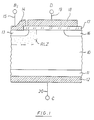
- a substrate 10 consists of n-type Silicon, to which an n+ region 11 with a collector metallization 12 connects at the bottom. From the main surface, a p-type base zone is diffused, over which a base metallization 14 is attached and on which a base connection 15 for the base B 1 of the power transistor T 1 of a Darlington circuit is shown schematically.
- a space charge zone RLZ is shown in broken lines.
- a diffused n+ zone 16 is also shown.
- the area between the zones 13 and 16 is covered over an insulating silicon oxide layer 17 by a metallization acting as a cover electrode 18, to which a schematic external connection 19 is also shown.
- a metallization acting as a cover electrode 18 is also shown.
- an external connection 20 is also on the collector metallization 12 to a common collector C of the power transistor T1 and the driver transistor T2 of the Darlington circuit.
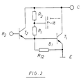
- Fig. 2 the electrical circuit diagram of the arrangement of FIG. 1 is shown supplemented by a voltage divider. It can be seen that between the common collector terminal C and between the base terminal B1 of the power transistor T1, a voltage divider from the resistors R1 and R2 is attached, the cover electrode 18 having connection to the center tap of this voltage divider. Through this connection, the cover electrode receives a potential that depends on the size of the resistors R1 and R2 and their ratio. From Fig. 1 it can be seen that the potential of the top electrode 18 acts on the space charge RLZ and thus influences and determines the collector-emitter breakdown voltage, a further dependency being given by the thickness of the silicon oxide layer 17.
- the uppermost point can be, for example, at 400 V and the start of the left curve branch, for example at 180 V.
- values T 1 and T 2 are each an operating point 1 and an operating point 2 at the corresponding breakdown voltages U CE1 and U CE2 in the left curve area. Working points in the right curve area lead to unstable conditions.
- the operating points shown are also not absolutely stable when choosing a circuit arrangement according to FIG. 2 and can change due to temperature dependencies, long-term drifts, tension during assembly, etc.
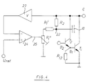
- a sufficient stabilization of the breakdown voltage U CE is made possible with the circuit expansion according to the invention according to FIG. 4, which can also be integrated on the Darlington chip.
- a voltage divider is provided, similar to that in Fig. 2, the resistor R2 with the collector C. and the divider tap 22 connected to the cover electrode 18 has connection.
- the resistor R1 is divided here into a fixed resistor R1 'and a controllable, variable resistor R1 ⁇ , which, however, is no longer connected to the base line to the power transistor, but to ground.
- the voltage applied to the collector C is suitably transformed, for example amplified via an amplifying element 23, and fed to a comparator or controller 24 as the actual value.
- a reference voltage U ref is applied to this regulator element 24 as the setpoint.
- a signal for adjustment is sent via a control line 25 of the resistance R1 ⁇ delivered. This changes the potential of the cover electrode 18 and thus also changes the breakdown voltage U CE .
- R1 ⁇ 0 ... R1 ⁇ Max R1 ′ + R1 ⁇ Max ⁇ R2.
- Fig. 4 the control circuit is shown in connection with the resistor R1. A control intervention via R2 is possible accordingly.
- FIG. 4 schematically represents the general control principle for setting the transistor breakdown voltage. Specific embodiments in which the circuit parts can be monolithically integrated in the Darlington chip are shown below in FIGS. 5 and 6.
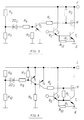
- FIGS. 5 and 6 represent the circuits according to the invention.
- Fig. 5 again the power transistor T1 with its base B1 and the driver transistor T2 with its base B2 can be seen.
- the voltage divider from the resistors R1 and R2 is similar to that in Fig. 4 with the resistor R2 connected to the collector C and the top electrode 18 on the divider tap.
- the resistor R1 is on the collector-emitter path of a transistor T3 to ground.
- a voltage divider from the resistors R5 and R6 is connected with its divider tap, the resistor R5 being connected to ground and following the resistor R6 a Z-diode ZD2, which in turn is connected to the voltage tap of a further voltage divider from the resistors R3 and R4 has connection.
- the resistor R3 is connected to ground, while the resistor R4 has the common collector C of the transistors T1 and T2 connection.
- the divider intervention on the voltage divider R1 / R2 takes place here the controlled current / voltage source from the collector-emitter voltage / current of the transistor T3.
- the breakdown voltage U CE is divided over the voltage divider from the resistors R3 and R4 and compared with a reference voltage.
- the voltage drop across the breakdown-operated Zener diode ZD2, the resistor R6 and the base-emitter voltage of the transistor T3 serves as the reference voltage.
- the value and the temperature behavior of the reference voltage can be optimized via the divider ratio of the resistors R5 and R6.
- the power transistor T1 with its base B1 and the driver transistor T2 with its base B2 and the common collector C can be seen.
- the voltage divider from the resistors R1 and R2 is provided with the connection of the divider tap to the cover electrode 18.
- the resistor R1 is here connected to the base of the power transistor T1
- the resistor R2 is the controlled current / voltage source as a collector-emitter - Voltage / current of the transistor T4 is connected downstream.
- the breakdown voltage U CE divided down by a voltage divider from the resistors R9 and R10 is also compared here with a reference voltage.
- the voltage drop across a Z-diode ZD3 and a Z-diode ZD3 connected downstream resistor R8 and the base-emitter voltage of a transistor T5 also serves as the reference voltage here.
- the resistor R8 is part of a voltage divider with a further resistor R7, which has a connection to the collector C.
- the value and the temperature behavior of the reference voltage can also be optimized here using the divider ratio R7 / R8.
Landscapes
- Engineering & Computer Science (AREA)
- Power Engineering (AREA)
- Bipolar Integrated Circuits (AREA)
- Bipolar Transistors (AREA)
- Amplifiers (AREA)
Abstract
Claims (2)
- Montage Darlington comprenant un transistor de puissance (T₁) et un transistor de commande (T₂) dont le collecteur est relié au collecteur du transistor de puissance (T₁), le transistor de puissance (T₁) et le transistor de commande (T₂) étant intégrés de manière monolithique en technique planaire dans un support (10) d'une plaquette formant les zones de collecteur des deux transistors (T₁, T₂), avec une résistance de sortie de base (R₁₂) montée entre la base (B₁) et l'émetteur (E) du transistor de puissance (T₁), une métallisation (18) formant une électrode de recouvrement, isolée électriquement par une couche d'oxyde de silicium (17) au-dessus de la zone de charge d'espace (RLZ) qui se développe dans la zone de la jonction pn sur la face supérieure de la plaquette entre la base et le collecteur, un diviseur de tension (résistances R₁ et R₂) avec une liaison de la prise médiane du diviseur de tension (R₁/R₂) et de la métallisation de l'électrode de recouvrement (18), le potentiel électrique de la métallisation (18) de l'électrode de recouvrement réglant la tension de claquage du transistor (tension de claquage collecteur-émetteur UCE) dont le potentiel est défini par le réglage du diviseur de tension (R₁/R₂), caractérisé en ce que ce potentiel et ainsi la tension de claquage (UCE), sont réglés par une tension de référence supplémentaire, les résistances (R₁/R₂) du diviseur de tension étant reliées par une source de courant/tension commandée, à la base (B₁) du transistor de puissance (T₁) ou du collecteur commun (C).
- Montage Darlington selon la revendication 1, caractérisé en ce que la source de courant/tension se compose de transistors (T₃ ; T₄, T₅) dont la commande de base comprend une diode de type Z (ZD₂ ; ZD₃) travaillant en claquage, et en ce que sa tension de claquage, avec la tension d'une résistance en aval (R₆ ; R₈) et celle du chemin base-émetteur d'un transistor (T₃ ; T₅), constitue la tension de référence pour la source de courant/tension, commandée, tension de référence à laquelle on compare la tension de claquage (UCE) divisée par un autre diviseur de tension (R₃ et R₄ ; R₉ et R₁₀).
Applications Claiming Priority (3)
| Application Number | Priority Date | Filing Date | Title |
|---|---|---|---|
| DE3926888A DE3926888A1 (de) | 1989-08-16 | 1989-08-16 | Darlington-transistorschaltung |
| DE3926888 | 1989-08-16 | ||
| PCT/DE1990/000575 WO1991003101A1 (fr) | 1989-08-16 | 1990-07-27 | Montage de darlington |
Publications (2)
| Publication Number | Publication Date |
|---|---|
| EP0572377A1 EP0572377A1 (fr) | 1993-12-08 |
| EP0572377B1 true EP0572377B1 (fr) | 1995-06-21 |
Family
ID=6387128
Family Applications (1)
| Application Number | Title | Priority Date | Filing Date |
|---|---|---|---|
| EP90911279A Expired - Lifetime EP0572377B1 (fr) | 1989-08-16 | 1990-07-27 | Montage de darlington |
Country Status (5)
| Country | Link |
|---|---|
| EP (1) | EP0572377B1 (fr) |
| JP (1) | JPH04507331A (fr) |
| KR (1) | KR920704417A (fr) |
| DE (2) | DE3926888A1 (fr) |
| WO (1) | WO1991003101A1 (fr) |
Families Citing this family (1)
| Publication number | Priority date | Publication date | Assignee | Title |
|---|---|---|---|---|
| CN104460815B (zh) * | 2014-04-30 | 2016-06-22 | 贵州航天凯山石油仪器有限公司 | 一种高温宽输入高精度电源 |
Family Cites Families (5)
| Publication number | Priority date | Publication date | Assignee | Title |
|---|---|---|---|---|
| IT1049596B (it) * | 1975-09-18 | 1981-02-10 | Ates Componenti Elettron | Dispositivo di protezione per un elemento di potenza di un circuito integrato |
| US4355341A (en) * | 1980-06-30 | 1982-10-19 | Rca Corporation | Power protection circuit for transistors |
| DE3227536A1 (de) * | 1982-01-20 | 1983-07-28 | Robert Bosch Gmbh, 7000 Stuttgart | Darlington-transistorschaltung |
| GB2138495B (en) * | 1983-03-26 | 1987-02-18 | Motorola Inc | Automotive ignition systems |
| JPS60126919A (ja) * | 1983-12-14 | 1985-07-06 | Toshiba Corp | ダ−リントントランジスタ回路 |
-
1989
- 1989-08-16 DE DE3926888A patent/DE3926888A1/de not_active Withdrawn
-
1990
- 1990-07-27 JP JP2510486A patent/JPH04507331A/ja active Pending
- 1990-07-27 WO PCT/DE1990/000575 patent/WO1991003101A1/fr not_active Ceased
- 1990-07-27 DE DE59009305T patent/DE59009305D1/de not_active Expired - Fee Related
- 1990-07-27 KR KR1019920700311A patent/KR920704417A/ko not_active Withdrawn
- 1990-07-27 EP EP90911279A patent/EP0572377B1/fr not_active Expired - Lifetime
Also Published As
| Publication number | Publication date |
|---|---|
| WO1991003101A1 (fr) | 1991-03-07 |
| EP0572377A1 (fr) | 1993-12-08 |
| DE59009305D1 (de) | 1995-07-27 |
| DE3926888A1 (de) | 1991-02-21 |
| JPH04507331A (ja) | 1992-12-17 |
| KR920704417A (ko) | 1992-12-19 |
Similar Documents
| Publication | Publication Date | Title |
|---|---|---|
| DE3141714C2 (fr) | ||
| DE69515417T2 (de) | IGBT-Treiberschaltung und Zündvorrichtung | |
| EP0281684B1 (fr) | Commutateur à transistors Darlington protégé contre des surtensions | |
| DE69508735T2 (de) | Vor Überströmen geschützter Leistungsschalter | |
| DE69617369T2 (de) | Verstärkerschaltung mit variabler Verstärkung | |
| DE4334513C1 (de) | CMOS-Schaltung mit erhöhter Spannungsfestigkeit | |
| DE68928176T2 (de) | Leistungshalbleitervorrichtung | |
| EP0144978A2 (fr) | Montage pour la commande d'un thyristor à l'aide d'un phototransistor | |
| DE69325278T2 (de) | Nichtflüchtige, elektrisch programmierbare Halbleiterspeicheranordnung mit einem Spannungsregler | |
| EP0174473B1 (fr) | Etage de sortie de puissance intégré monolithiquement | |
| DE69121254T2 (de) | Aktive Überbrückung zur Verhinderung von Hochfrequenzversorgungsschwankungen in integrierten Schaltungen | |
| EP1284019B1 (fr) | Composant semi-conducteur de puissance | |
| DE2635218A1 (de) | Anordnung zum schutz eines transistors | |
| DE4300953A1 (en) | Temp.-stabilised electronic ignition for IC engine - has series opposition Zener diodes between base of control transistor and earth | |
| DE69815289T2 (de) | Spannungsreglerschaltungen und halbleiterschaltung | |
| EP0572377B1 (fr) | Montage de darlington | |
| DE10301693B4 (de) | MOSFET-Schaltung mit reduzierten Ausgangsspannungs-Schwingungen bei einem Abschaltvorgang | |
| DE102005010013B4 (de) | Stromregler mit einem Transistor und einem Messwiderstand | |
| DE60004008T2 (de) | Halbleiterschaltung mit einem Bauelement mit isoliertem Gate und einer zugehörigen Kontrollschaltung | |
| DE102020128289B4 (de) | Halbleitervorrichtung | |
| EP0181355B1 (fr) | Dispositif semiconducteur monolithique a structure plane | |
| DE10139515C2 (de) | Bandabstandsschaltung | |
| DE2722248C3 (de) | Elektronischer Schalter für induktive Last | |
| DE1513364A1 (de) | Hochstromregler mit negativem Widerstand | |
| EP0990199B1 (fr) | Dispositif de reglage |
Legal Events
| Date | Code | Title | Description |
|---|---|---|---|
| PUAI | Public reference made under article 153(3) epc to a published international application that has entered the european phase |
Free format text: ORIGINAL CODE: 0009012 |
|
| 17P | Request for examination filed |
Effective date: 19920117 |
|
| AK | Designated contracting states |
Kind code of ref document: A1 Designated state(s): DE FR GB IT |
|
| 17Q | First examination report despatched |
Effective date: 19940725 |
|
| GRAA | (expected) grant |
Free format text: ORIGINAL CODE: 0009210 |
|
| AK | Designated contracting states |
Kind code of ref document: B1 Designated state(s): DE FR GB IT |
|
| ET | Fr: translation filed | ||
| REF | Corresponds to: |
Ref document number: 59009305 Country of ref document: DE Date of ref document: 19950727 |
|
| ITF | It: translation for a ep patent filed | ||
| GBT | Gb: translation of ep patent filed (gb section 77(6)(a)/1977) |
Effective date: 19950829 |
|
| PLBE | No opposition filed within time limit |
Free format text: ORIGINAL CODE: 0009261 |
|
| STAA | Information on the status of an ep patent application or granted ep patent |
Free format text: STATUS: NO OPPOSITION FILED WITHIN TIME LIMIT |
|
| 26N | No opposition filed | ||
| REG | Reference to a national code |
Ref country code: GB Ref legal event code: IF02 |
|
| PGFP | Annual fee paid to national office [announced via postgrant information from national office to epo] |
Ref country code: GB Payment date: 20020711 Year of fee payment: 13 |
|
| PGFP | Annual fee paid to national office [announced via postgrant information from national office to epo] |
Ref country code: FR Payment date: 20020723 Year of fee payment: 13 |
|
| PG25 | Lapsed in a contracting state [announced via postgrant information from national office to epo] |
Ref country code: GB Free format text: LAPSE BECAUSE OF NON-PAYMENT OF DUE FEES Effective date: 20030727 |
|
| GBPC | Gb: european patent ceased through non-payment of renewal fee |
Effective date: 20030727 |
|
| PG25 | Lapsed in a contracting state [announced via postgrant information from national office to epo] |
Ref country code: FR Free format text: LAPSE BECAUSE OF NON-PAYMENT OF DUE FEES Effective date: 20040331 |
|
| REG | Reference to a national code |
Ref country code: FR Ref legal event code: ST |
|
| PG25 | Lapsed in a contracting state [announced via postgrant information from national office to epo] |
Ref country code: IT Free format text: LAPSE BECAUSE OF NON-PAYMENT OF DUE FEES;WARNING: LAPSES OF ITALIAN PATENTS WITH EFFECTIVE DATE BEFORE 2007 MAY HAVE OCCURRED AT ANY TIME BEFORE 2007. THE CORRECT EFFECTIVE DATE MAY BE DIFFERENT FROM THE ONE RECORDED. Effective date: 20050727 |
|
| PGFP | Annual fee paid to national office [announced via postgrant information from national office to epo] |
Ref country code: DE Payment date: 20050916 Year of fee payment: 16 |
|
| PG25 | Lapsed in a contracting state [announced via postgrant information from national office to epo] |
Ref country code: DE Free format text: LAPSE BECAUSE OF NON-PAYMENT OF DUE FEES Effective date: 20070201 |