EP0570128B1 - Verketteter Behälter zum Transportieren von Präzisionsvorrichtungen - Google Patents
Verketteter Behälter zum Transportieren von Präzisionsvorrichtungen Download PDFInfo
- Publication number
- EP0570128B1 EP0570128B1 EP93303289A EP93303289A EP0570128B1 EP 0570128 B1 EP0570128 B1 EP 0570128B1 EP 93303289 A EP93303289 A EP 93303289A EP 93303289 A EP93303289 A EP 93303289A EP 0570128 B1 EP0570128 B1 EP 0570128B1
- Authority
- EP
- European Patent Office
- Prior art keywords
- unit
- container
- arms
- transverse
- arm
- Prior art date
- Legal status (The legal status is an assumption and is not a legal conclusion. Google has not performed a legal analysis and makes no representation as to the accuracy of the status listed.)
- Expired - Lifetime
Links
Images


Classifications
-
- H—ELECTRICITY
- H01—ELECTRIC ELEMENTS
- H01L—SEMICONDUCTOR DEVICES NOT COVERED BY CLASS H10
- H01L21/00—Processes or apparatus adapted for the manufacture or treatment of semiconductor or solid state devices or of parts thereof
- H01L21/67—Apparatus specially adapted for handling semiconductor or electric solid state devices during manufacture or treatment thereof; Apparatus specially adapted for handling wafers during manufacture or treatment of semiconductor or electric solid state devices or components ; Apparatus not specifically provided for elsewhere
- H01L21/68—Apparatus specially adapted for handling semiconductor or electric solid state devices during manufacture or treatment thereof; Apparatus specially adapted for handling wafers during manufacture or treatment of semiconductor or electric solid state devices or components ; Apparatus not specifically provided for elsewhere for positioning, orientation or alignment
-
- H—ELECTRICITY
- H05—ELECTRIC TECHNIQUES NOT OTHERWISE PROVIDED FOR
- H05K—PRINTED CIRCUITS; CASINGS OR CONSTRUCTIONAL DETAILS OF ELECTRIC APPARATUS; MANUFACTURE OF ASSEMBLAGES OF ELECTRICAL COMPONENTS
- H05K13/00—Apparatus or processes specially adapted for manufacturing or adjusting assemblages of electric components
- H05K13/0084—Containers and magazines for components, e.g. tube-like magazines
-
- H—ELECTRICITY
- H01—ELECTRIC ELEMENTS
- H01L—SEMICONDUCTOR DEVICES NOT COVERED BY CLASS H10
- H01L2221/00—Processes or apparatus adapted for the manufacture or treatment of semiconductor or solid state devices or of parts thereof covered by H01L21/00
- H01L2221/67—Apparatus for handling semiconductor or electric solid state devices during manufacture or treatment thereof; Apparatus for handling wafers during manufacture or treatment of semiconductor or electric solid state devices or components; Apparatus not specifically provided for elsewhere
- H01L2221/683—Apparatus for handling semiconductor or electric solid state devices during manufacture or treatment thereof; Apparatus for handling wafers during manufacture or treatment of semiconductor or electric solid state devices or components; Apparatus not specifically provided for elsewhere for supporting or gripping
- H01L2221/68304—Apparatus for handling semiconductor or electric solid state devices during manufacture or treatment thereof; Apparatus for handling wafers during manufacture or treatment of semiconductor or electric solid state devices or components; Apparatus not specifically provided for elsewhere for supporting or gripping using temporarily an auxiliary support
- H01L2221/68309—Auxiliary support including alignment aids
-
- H—ELECTRICITY
- H01—ELECTRIC ELEMENTS
- H01L—SEMICONDUCTOR DEVICES NOT COVERED BY CLASS H10
- H01L2221/00—Processes or apparatus adapted for the manufacture or treatment of semiconductor or solid state devices or of parts thereof covered by H01L21/00
- H01L2221/67—Apparatus for handling semiconductor or electric solid state devices during manufacture or treatment thereof; Apparatus for handling wafers during manufacture or treatment of semiconductor or electric solid state devices or components; Apparatus not specifically provided for elsewhere
- H01L2221/683—Apparatus for handling semiconductor or electric solid state devices during manufacture or treatment thereof; Apparatus for handling wafers during manufacture or treatment of semiconductor or electric solid state devices or components; Apparatus not specifically provided for elsewhere for supporting or gripping
- H01L2221/68304—Apparatus for handling semiconductor or electric solid state devices during manufacture or treatment thereof; Apparatus for handling wafers during manufacture or treatment of semiconductor or electric solid state devices or components; Apparatus not specifically provided for elsewhere for supporting or gripping using temporarily an auxiliary support
- H01L2221/68313—Auxiliary support including a cavity for storing a finished device, e.g. IC package, or a partly finished device, e.g. die, during manufacturing or mounting
-
- Y—GENERAL TAGGING OF NEW TECHNOLOGICAL DEVELOPMENTS; GENERAL TAGGING OF CROSS-SECTIONAL TECHNOLOGIES SPANNING OVER SEVERAL SECTIONS OF THE IPC; TECHNICAL SUBJECTS COVERED BY FORMER USPC CROSS-REFERENCE ART COLLECTIONS [XRACs] AND DIGESTS
- Y10—TECHNICAL SUBJECTS COVERED BY FORMER USPC
- Y10S—TECHNICAL SUBJECTS COVERED BY FORMER USPC CROSS-REFERENCE ART COLLECTIONS [XRACs] AND DIGESTS
- Y10S206/00—Special receptacle or package
- Y10S206/82—Separable, striplike plural articles
Definitions
- the present invention relates to a linked container for transporting the precision devices such as the IC chips, the various electronic devices (for example, connectors, switches, transmitters and the like ) and the comparatively small precision parts incorporated in precision machines ( herein inclusively referred to as "IC chips" ), wherein the IC chips take their individual and discrete places within the container.
- the precision devices such as the IC chips, the various electronic devices (for example, connectors, switches, transmitters and the like ) and the comparatively small precision parts incorporated in precision machines ( herein inclusively referred to as "IC chips" ), wherein the IC chips take their individual and discrete places within the container.
- the important or principal electronic circuits are delivered nowadays in the form of the so-called "chip" in order to improve their operation reliability as well as the efficiency of assembly plants.
- the preliminary and/or final assembly lines are supplied with the IC chips which are arrayed in a considerably large transporting container, which has a plurality of chip-holding recesses forming longitudinal and transverse rows.
- a robot hand or the like equipped beside one side of a transporting route supplies the IC chips one by one from the large container to the assembly line. Therefore, the robot hand must reciprocate a long distance in order to pick up the IC chip positioned near the other side of the transporting route. Consequently, an average waiting time for the assembly line to receive the individual IC chips becomes long to thereby lower the production efficiency.
- the robot hand must change its position every time when it picks up the IC chips. In the event that the robot hand fails to grip any IC chip at its correct portion, the IC chip would be broken and the assembly line would be disturbed seriously. In order to avoid such an incident, the position control of robot hand should be so accurate as undesirably raising the control system cost.
- the phantom lines "C" in Fig. 16 indicate an inevitable curvature remaining in the band unwound from the reel.
- the unwound band cannot take again its absolutely straight position indicated by the solid lines "D".
- the curled band will cause a miss-operation of the robot hand which must exactly pick up the IC chips one by one. If the recess walls were rendered as thin as possible to eliminate such a drawback, then another problem would arise that the band becomes so fragile and are broken when handled, thus failing to afford a sufficient protection to the band. A damaged transporting band will also hinder the IC chips from being picked up in an accurate manner.
- trays Another disadvantage inherent in the prior art containers ( here called “trays” ) is that they occupy much space for storage and handling, and require much labour for replacement of some unit trays with new ones. In addition, it is not necessarily easy to supply the unit trays in any desirable linked form. Further, the trays for the IC chips of some kinds have to withstand a necessary baking treatment, thereby raising the manufacture cost of the trays.
- An object of the present invention which was made to eliminate the drawbacks in the prior art container for transporting precision devices arranged therein in longitudinal and transverse rows or in a single longitudinal row, is therefore to provide a linked container composed of a plurality of repeating units of the substantially same shape like a chain widely used in the machinery, wherein the repeating units have recesses to respectively receive the IC chips or the like and are connected one to another to form an endless band.
- Another object of the invention is to provide a linked container composed of the repeating units each having a recess for stably holding therein each IC chip, wherein each unit comprises connected arms outwardly extending from its opposite sides to link the units capable of flexing relative to one another, so that they can more easily be wound on a reel without causing any curvature to remain in the band unwound therefrom.
- Still another object is to provide a linked container which is free from the disadvantages in the prior art trays, and can withstand the baking treatment together with the IC chips held therein, thus enabling the baked trays to be recycled.
- the invention provides a linked container for transporting precision devices, the container comprising a row of repeating units made of a plastics and shaped to receive transported devices within recesses; each unit having along at least one of opposite lateral sides a row of portions arranged at regular intervals, with the portions being engageable with and disengageable from driving lugs of a stepping driver, each unit defining at least one of the recesses and having opposite transverse sides "A” and "B", junctions each formed between the side "A" of one unit and the side "B” of the next unit; and characterised in that each junction is a hinge which allows the juxtaposed adjacent sides "A” and “B” to rotate relative to and in parallel with each other and each recess has finger-shaped lugs protruding from within for holding a device therebetween.
- a linked container which is provided herein for transporting precision devices and constructed in such a manner as to achieve the objects, does characteristically comprise a flexible band having: series of recesses (11) arranged along the band for receiving transported articles; and a row of small apertures (14) along at least one of opposite sides (12, 13) of the band, with the apertures (14) being arranged at regular intervals along the full length of the band, and engageable with and disengageable from driving lugs of a stepping driver; the flexible band being a row of repeating plastics units (10) which are of the same dimension at least in the longitudinal direction of the band; each unit (10) defining at least one recess (11) and having opposite transverse sides "A” and "B", the band further comprising junctions each formed between the side "A" of one unit (10) and the side "B” of the next unit; and, the junction being a hinge (22,24; 51,52; 22e,24e,57) which allows the juxtaposed adjacent sides "A" and "
- each recess and outer walls surrounding it are shaped square or rectangular, one of the sides "A" of one unit is kept along its full length close to the full length of the other side "B" of the next unit, whether they are bent or stretched. It is noted however that depth, configuration and/or dimension in plan view of the recess, formed generally centrally of each unit according to a preferred embodiment, does depend on the shape and dimension of the articles such as IC chips which are to be received in the recess. In one example, the recess is about 15 mm square and 3 mm deep, and its surrounding walls excluding any arm which may extend therefrom have a dimension of 24 mm x 20 mm.
- the recess need not be square or rectangular in plan view, but may be elliptic or polygonal.
- the hinge is interposed between two adjacent repeating units each formed with the recess so that they can be bent and stretched freely and readily.
- a hinge comprises, for each side of the unit, a pair of two arms extending in opposite directions along two parallel lines perpendicular to the sides facing one another.
- a small protrusion is formed near and integral with an end of each arm from the one side, so as to protrude transversely in parallel therewith.
- a transverse opening is provided near and integral with an end of each arm from the other side, so that each protrusion mates with the corresponding opening.
- Two small protrusions may be disposed in the same direction, or alternatively in opposite directions.
- annular groove is formed around each transverse protrusion which is a short rod in parallel with one side of the unit, and each arm extending from the other side has a lower portion formed with a cutout. An inner region of this cutout is fitted on the grooved protrusion to be rotatable relative thereto, while an outer region continued from the inner region however being slightly narrower than it.
- a spherical protrusion is formed at the end of each arm from one side of the unit, and an upwardly opened cavity is formed in a cubic end of each of other arms from the other side. This cavity is defined by a vertical outer region or slit of a width slightly larger than the diameter of the former arms.
- the slit is continued to an inner region of a width slightly smaller than the diameter of the spherical protrusion, and has an enlarged, generally spherical space formed at a middle height of the inner region.
- the enlarged space is of such a dimension as permitting the protrusion to fit therein, thereby constructing a kind of ball joint.
- two arms extend from one of the adjacent sides facing one another, along two lines perpendicular to the sides. At least one arm extend from the other side, likewise along the lines, wherein transverse openings penetrate end portions of those arms and are in alignment with one another to receive therethrough a pin.
- tabs outwardly protrude from and integral with the opposite sides of each unit so as to extend in parallel with a plane including the facing sides. A straight crease or fold intervenes each side and the tab extending therefrom, and these tabs belonging to the adjacent units are overlaid and fixedly adjoined one to another. It is noted here that each unit may have two or more recesses which are arranged to provide one or more rows between and along the sides "A" and "B".
- the apertures for example round apertures, engaging with the driver of the transporting mechanism may be arranged to form a single row along one of lateral sides of the band, or to form two rows along the respective sides.
- the round apertures are disposed at regular intervals, that is at a given pitch, in an intermediate region between the transverse sides.
- a cutout corresponding to a half of the aperture is formed at each corner where the transverse side intersects the lateral side.
- two cutouts can constitute a single recessed region of a width equal to the diameter of said aperture when the adjacent transverse sides are juxtaposed, whereby the pitch of the apertures is not disturbed between the neighboring units.
- any cutout may not be formed through the abutting sides, but the distance from each transverse side to the nearest aperture may be half a distance between two apertures, thereby also avoiding any irregularity in the aperture pitch.
- All the apertures engaging with the sprocket or other stepping drive may not be circular holes but may be cutouts extending inwardly from the lateral sides, or any small lugs protruding upwardly, downwardly or outwardly from said lateral sides.
- a hole may be formed through the central bottom portion of each recess so that the IC chip can be ejected by an ejector pin upon arrival at destination.
- Those central holes may preferably so bigger than the side apertures as allowing a thick ejector pin to gently push the IC chip.
- the recess bottom may be formed with a pair of finger-shaped lugs which hold therebetween such a protrusion.
- An additional hole which will function similarly to the central hole, may penetrate the region of recess bottom between said lugs.
- the linked container constructed as above comprises a number of the repeating units which can be mass-produced by the injection molding of a suitable plastics. Every unit can be connected to the next one, by forcibly clicking the small protrusions at the arm ends at the transverse side "A" into the apertures at the other arm ends at the other side "B". This operation to form the hinge at junction between two units will be repeated many times to provide the container of a given length.
- the linked container provided herein will operate in the same manner as the prior art containers, but much more smoothly when wound on and unwound from a reel, by virtue of the chain-like hinge which facilitate the bending and stretching between the adjacent units. Such a hinge is effective also to prevent any curvature from remaining in the stretched container.
- the container whose chain length may previously be adjusted, can be heat treated in a baking oven for the processing of IC chips in the container.
- FIG. 1 A linked container for transporting precision devices is shown in Figs. 1 to 5.
- This container is produced by injection molding a polystyrol resin, and assumes a band as shown in Fig. 2, wherein it comprises a row of recesses 11 each for receiving an IC chip ( i.e., a small-sized integrated circuit formed on a wafer ) as an example of the articles to be transported.
- the stepping driver's lugs (not shown ) in a transportation system are adapted to engage with a plurality of apertures 14 arranged along one lateral side 12 of the band at regular intervals over its full length.
- Fig. 1 shows that the linked container provided herein does characteristically comprise repeating units 10 each having the recess 11 formed centrally thereof.
- the recess 11 is a concave portion which is surrounded by a peripheral flange 15 having a width of 2 - 4 mm, and recessed downwardly in the drawings.
- Each unit 10 has transverse sides "A” and "B” opposite one to another, and walls 16 and 17 under the flange 15.
- Two pairs of arms 21 and 21, and 23 and 23, are integral with the walls 16 and 17, respectively, and extend outwardly along the imaginary lines "L” and "M” perpendicular to the transverse sides. Those arms construct junctions of the hinge type between two adjacent units 10 and 10, as will be detailed later.
- a short columnar protrusion 22 is formed integral with the end portion of each arm 21 from one side "A", and those protrusions have their extremity rounded and extend outwardly in opposite directions.
- a transverse opening 24 is formed through the end portion of each of the other arms 23 from the other side "B".
- the respective protrusions 22 can click in an elastic manner into the openings 24.
- the diameter of such protrusions and openings is about 1.2 mm.
- the protrusions 22 thus clicked into the openings 24 build the hinge for connecting the adjacent units, so that the arms 21 are bendable and stretchable relative to the mating arms 23.
- a distance between the axes of the protrusion 22 and opening 24 disposed near one lateral side 12 is equal to the distance between the other axes of those protrusion and opening near the other lateral side 13. This feature ensures the free bending of the band at its portion between the adjacent units 10 and 10 as shown in Figs. 3 and 5.
- a cutout 19 in Fig. 1 is formed at the unit's corner where the transverse side "A" or "B" intersect the lateral side 12 or 13.
- Two adjacent cutouts 19 are shaped complementary with one another to provide a slot which functions as if it were one of the side apertures 14. In other words, such a configuration of cutouts at the junction between the adjacent units is also effective to drive the container to advance forwards.
- the linked container described above will be used in the following manner as shown in Figs. 1, 4 and 5.
- the articles carried by the container are, for example, a number of square IC chips 40.
- Each IC chip has a plurality of input-output pins 41 protruding from each side. Those chips will be inserted into the recesses 11 as indicated by the phantom line "Y" in Fig. 1, wherein the bent ends of the pins 41 will bear against the inner surfaces of the walls 16 and 17.
- the body 42 of each chip will closely fit in a low compartment defined by low ridges 31 formed upright from the bottom 30 of recess and along the four sides thereof. After insertion, a protective film 33 will cover each recess and be adhered to the peripheral flange 15.
- This film protects the received article from any dust and also from unintentional slippage out of the recess 11 while this container is transported or handled.
- the linked container carrying the chips will be bent at junctions between the units as shown at "R” in Fig. 3 when wound on a reel (not shown ) in a manner shown in Fig. 5. Such a reel will be delivered to any desired station on the assembly line or any processing line.
- the linked container will be pulled off the reel as indicated by "T” at said station so that the units successively advances onto a common flat plane as indicated by "S”.
- an ejector pin will be thrust through the round hole 32 of the bottom 30 so as to unload the chip out of the recess 11.
- a robot arm disposed near the given location will thus pick up the chip and move it onto any desired location on the assembly line.
- the precision devices such as IC chips in the recesses each sealed with a cover tape (i.e., protective film ) are supplied to a "surface mounting machine", and this machine ejects with its pin the devices and subsequently positions them one by one to the designed portions on a circuit board.
- the container in a first embodiment of the present invention is shown in Figs. 6 to 8. It comprises rectangular recesses 11 and two rows of apertures 14 arranged along both the lateral sides 12 and 13, with the apertures being engageable with sprockets or the like. Since the chip as an example of the article accommodated in each recess has a round body 42 and ears 43 and 44, the low ridges 31 ( gripping the chip body in the foregoing example) are replaced with pairs of parallel fingers 34 or oblique fingers 35 which grip the ears. Bumps 36 are formed at upper ends of at least one pair of fingers 34 so as to face one another, so that the ear will be retained between the fingers and the bottom 30, thus preventing the chip from slipping off the recess 11. In this manner, the devices such as IC chips are secured by the ears to the bottoms of recesses 11 (i.e., "pockets" ) of the repeating units 10.
- the flanges 15 in both the first embodiment and the foregoing example is about 0.4 mm thick, but the bottom 30 and the walls 16 and 17 are about 0.7 mm thick. Such thicker bottom and walls, which will not be deformed during the operation of those containers, give a surer protection to the accommodated articles. Further, those containers can be used again if required, though they have generally been thrown away after used one time. It will be understood that the number of the repeating units in the container of the invention may be changed easily when it is recycled.
- a spherical protrusion 22 is formed at the end of each arm 21 from one side of the unit, and a cavity is formed in cubic arms 23 from the other side. This cavity is defined by a vertical outer slit 24c of a width slightly larger than the diameter of the former arm 23.
- the slit 24c of each arm 23 is continued to an inner region 24b of a width slightly smaller than the diameter of the spherical protrusion 22.
- This inner region has an enlarged, generally spherical space 24d formed at its middle height and having such a dimension as allowing the protrusion to fit therein.
- the former arm 21 is to be pressed against the latter arm in a direction indicated by the arrow "P", thereby causing the protrusion 22 to click into the enlarged space 24d so that the repeating units made of the elastic plastics can be readily connected one to another.
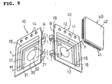
- small protrusions 22 extend in the same direction from the end portions of arms 21 which extend from one side "A".
- the other arms 23 from the other side "B” have their end portions formed with openings 24, and the protrusions 22 are caused to elastically fit therein slidably and rotatively relative thereto.
- Those protrusions 22 and openings 24 constitute a hinge, and the following unit need be just be caused to slide along the leading unit in order to provide a junction between them at their arms, thus rendering easier the assembly of the band-shaped linked container.
- extremities of the protrusions 22 have a diameter slightly greater than that of the openings 24, though not shown in Fig. 9. Due to this feature, the protrusions will not be removed from the openings if handled in a usual manner.
- two arms 21 extend from one transverse side, and also two arms 23 extend from the other side.
- Transverse openings 22e and 24e are formed to penetrate end portions of those arms and are in alignment with one another to receive therethrough a pin 57, which similarly constitutes together with the openings a hinge-like junction.
- the pin 57 fits very tightly in the openings through the inner arms 21, but loosely in those through the outer arms 23 so as to be rotatable therein.
- Base portions of the two inner arms may be integral with each other, or alternatively a single arm may take place of the two inner arms. Since the pin is adopted and the joint resembles the well known hinges, not only the operation for manufacturing the band-shaped container is easy, but also it can be bent and stretched very smoothly between its adjacent units.
- Fig. 12 shows tabs 51 outwardly protruding from and integral with the opposite sides "A" and "B" of each unit so as to extend in parallel with a plane including the facing sides.
- a straight crease or fold 52 intervenes each side and the tab extending therefrom, and these tabs 51 and 51 respectively belonging to the adjacent units 10 and 10 are overlaid one on another and fixedly adjoined one to another.
- Those tabs 51 and crease 52 construct the hinge type junction.
- the means for adjoining those tabs may be the spot welding, or the button-hook shown in a modification shown in Fig. 13. In this modification, round button-like lugs 54 are formed on one tab so that they are forced into small holes 55 through the other tab.
- this band can be wound to have a smaller diameter if the bottoms are laid inside the flange. It is not necessary in the examples shown in Figs. 12 and 13 to form any arm having a transverse opening. Thus, the injection molding of the repeating units is easier in this case, and besides their connection is not difficult.
- Fig. 14 shows in part a repeating unit, in which each unit has two recesses 11 in a row between the transverse sides "A" and "B".
- each unit 10 has eight recesses 11 which are arranged to form two rows each comprising four recesses.
- the driven apertures 14 are formed at regular intervals along each lateral sides of the container. This repeating unit is advantageous when the IC chips are considerably small compared with the repeating unit of the container, because a plurality of them can be accommodated in one unit to thereby improve the efficiency in feeding them to an assembly line of precision instruments.
- the protrusions of the arms from one transverse side may extend to face one another.
- the repeating units, especially their chip receiving recesses may be of any different shapes so long as they have the same length in the longitudinal direction of the container.
- the present invention offers a linked band-like container which is composed of a series of repeating units of a sufficient thickness.
- the container provided herein is most suited as a container for the IC chips or the like which must be handled carefully and positioned accurately after delivered to users and when treated with by them.
- units each having a rigid pocket are connected one to another to form a band which can be stretched without causing any curvature to remain when the thus carried devices are fed to a surface mounting machine operating at high precision.
Landscapes
- Engineering & Computer Science (AREA)
- Manufacturing & Machinery (AREA)
- Microelectronics & Electronic Packaging (AREA)
- Physics & Mathematics (AREA)
- Condensed Matter Physics & Semiconductors (AREA)
- General Physics & Mathematics (AREA)
- Computer Hardware Design (AREA)
- Power Engineering (AREA)
- Packaging Frangible Articles (AREA)
- Packaging Of Annular Or Rod-Shaped Articles, Wearing Apparel, Cassettes, Or The Like (AREA)
Claims (7)
- Verketteter Behälter zum Transportieren von Präzisionsvorrichtungen, wobei der Behälter folgende Komponenten umfaßt:eine Reihe von sich wiederholenden Einheiten (10), die aus Plast bestehen und so geformt sind, daß sie in Aussparungen (11) die transportierten Geräte aufnehmen können;wobei jede Einheit an wenigstens einem von gegenüberliegenden seitlichen Rändern (12, 13) eine Reihe von Abschnitten (14) hat, die in regelmäßigen Abständen angeordnet sind, wobei Mitnehmerzapfen eines Schrittantriebs in die Abschnitte eingreifen und aus dem Eingriff mit diesen gebracht werden können;wobei jede Einheit (10) wenigstens eine der Aussparungen (11) bildet und gegenüberliegende Querseiten "A" und "B" hat;Verbindungen, die jeweils zwischen der Seite "A" der einen Einheit (10) und der Seite "B" der nächsten Einheit gebildet werden; und dadurch gekennzeichnet, daßjede Verbindung ein Gelenk (22, 24; 51, 52; oder 22e, 24e. 57) ist. das es den aneinanderliegenden angrenzenden Seiten "A" und "B" ermöglicht, sich relativ zu- und parallel miteinander zu drehen, und daß jede Aussparung (11) fingerförmige Ösen (34, 35) hat, die von dieser vorstehen, um zwischen diesen ein Gerät zu halten.
- Verketteter Behälter nach Anspruch 1, bei dem das Gelenk zwischen benachbarten Einheiten (10) zusammengesetzt ist aus: zwei Paaren von Armen (21, 23). die von jeder Einheit nach außen und längs der imaginären Linien "L" und "M", die senkrecht zu den Querseiten "A" und "B" stehen, verlaufen: einem kurzen säulenförmigen und querverlaufenden Vorsprung (22), der mit dem Endabschnitt jedes Armes (21) von einer Seite "A" ein Ganzes bildet. wobei sich diese Vorsprünge in entgegengesetzte Richtungen oder in die gleiche Richtung erstrecken: und einer Queröffnung (24), die durchführend im Endabschnitt jedes der anderen Arme (23) von der anderen Seite "B" gebildet wird, so daß die entsprechenden Vorsprünge (22) in die entsprechenden Öffnung (24) einschnappen.
- Verketteter Behälter nach Anspruch 1, bei dem das Gelenk zwischen den benachbarten Einheiten (10) zusammengesetzt ist aus: einer ringförmigen Kehle (22a). die um einen Quervorsprung (22) jedes der Arme (21), der von einer Querseite "A" ausgeht, gebildet wird; einem unteren Abschnitt jedes der anderen Arme (23) von der anderen Seite "B", wobei der untere Abschnitt eine nach unten offene Aussparung (24) hat; und wobei ein innerer Bereich (24b) dieser Aussparung in die Kehle (22a) eingepaßt wird, um im Verhältnis zu dieser drehbar zu sein, wobei sich anschließend an den inneren Bereich ein äußerer Bereich (24c) fortsetzt und geringfügig schmaler als dieser ist, so daß der letztgenannte Arm (23) mit dem erstgenannten Arm zum Eingriff einschnappt.
- Verketteter Behälter nach Anspruch 1, bei dem das Gelenk zwischen den benachbarten Einheiten (10) zusammengesetzt ist aus: einem kugelförmigen Vorsprung (22), der am Ende jedes der Arme (21) von einer Seite "A" der Einheit gebildet wird; einem Hohlraum, der in jedem der kubischen Arme (23) von der anderen Seite "B" gebildet wird, wobei jeder Hohlraum gebildet wird durch einen senkrechten äußeren Schlitz (24c) mit einer Breite, die geringfügig größer als der Durchmesser des erstgenannten Arms (23) ist. wobei sich der Schlitz (24c) jedes Armes (23) in einem inneren Bereich (24b) mit einer Breite fortsetzt, die geringfügig kleiner als der Durchmesser des kugelförmigen Vorsprungs (22) ist, und der innere Bereich einen vergrößerten und allgemein kugelförmigen Raum (24d) hat, der bei seiner mittleren Höhe gebildet wird und so dimensioniert ist, daß der Vorsprung darin eingepaßt werden kann.
- Verketteter Behälter nach Anspruch 1, bei dem das Gelenk zwischen den benachbarten Einheiten (10) zusammengesetzt ist aus: zwei Armen (21). die von einer Querseite "A" der Einheit ausgehen; wenigstens einem Arm (23). der von der anderen Seite "B" der Einheit ausgeht; Queröffnungen (22e) und (24e), die so geformt sind, daß sie in Endabschnitte dieser Arme eindringen und miteinander ausgerichtet sind; und einem Stift (57), der in die ausgerichteten Öffnungen (22e, 24e) eingeführt ist.
- Verketteter Behälter nach Anspruch 1, bei dem das Gelenk zwischen den benachbarten Einheiten (10) zusammengesetzt ist aus: Leisten (51), die von den gegenüberliegenden Seiten "A" und "B" jeder Einheit vorstehen und mit diesen aus einem Ganzen bestehen, so daß sie parallel zu einer Ebene verlaufen, welche die zueinander gerichteten Seiten einschließt; und einer geraden Sicke oder Falz (52), welche zwischen jeder Seite und der von dieser ausgehenden Leiste liegt, wobei diese Leisten (51), die jeweils zu den angrenzenden Einheiten (10) gehören, sich gegenseitig überlagern und aneinander befestigt werden.
- Verketteter Behälter nach einem der Ansprüche 1 bis 6, bei dem jede Einheit 10 wenigstens zwei Aussparungen 11 hat. die so angeordnet sind, daß sie wenigstens eine Reihe zwischen den Querseiten "A" und "B" bilden.
Applications Claiming Priority (10)
| Application Number | Priority Date | Filing Date | Title |
|---|---|---|---|
| JP148231/92 | 1992-05-13 | ||
| JP14823192A JP2603581B2 (ja) | 1992-05-13 | 1992-05-13 | 精密部品搬送用の連鎖型容器 |
| JP4358445A JPH0767953B2 (ja) | 1992-12-25 | 1992-12-25 | 精密部品搬送用の連鎖型容器 |
| JP358446/92 | 1992-12-25 | ||
| JP358447/92 | 1992-12-25 | ||
| JP4358446A JPH0771985B2 (ja) | 1992-12-25 | 1992-12-25 | 精密部品搬送用の連鎖型容器 |
| JP358444/92 | 1992-12-25 | ||
| JP4358447A JPH0771986B2 (ja) | 1992-12-25 | 1992-12-25 | 精密部品搬送用の連鎖型容器 |
| JP4358444A JPH0710704B2 (ja) | 1992-12-25 | 1992-12-25 | 精密部品搬送用の連鎖型容器 |
| JP358445/92 | 1992-12-25 |
Publications (2)
| Publication Number | Publication Date |
|---|---|
| EP0570128A1 EP0570128A1 (de) | 1993-11-18 |
| EP0570128B1 true EP0570128B1 (de) | 1996-06-19 |
Family
ID=27527833
Family Applications (1)
| Application Number | Title | Priority Date | Filing Date |
|---|---|---|---|
| EP93303289A Expired - Lifetime EP0570128B1 (de) | 1992-05-13 | 1993-04-27 | Verketteter Behälter zum Transportieren von Präzisionsvorrichtungen |
Country Status (4)
| Country | Link |
|---|---|
| US (1) | US5333733A (de) |
| EP (1) | EP0570128B1 (de) |
| KR (1) | KR100285655B1 (de) |
| DE (1) | DE69303230D1 (de) |
Cited By (1)
| Publication number | Priority date | Publication date | Assignee | Title |
|---|---|---|---|---|
| DE102008042195A1 (de) | 2007-12-20 | 2009-06-25 | Patek Philippe Sa | Transportvorrichtung für Werkstücke |
Families Citing this family (36)
| Publication number | Priority date | Publication date | Assignee | Title |
|---|---|---|---|---|
| EP0660655B1 (de) * | 1993-12-27 | 1998-01-28 | GOLD INDUSTRIES Co. Ltd. | Behältereinrichtungen-Zusammenbau zum Transportieren von Präzisionsvorrichtung |
| JP3526625B2 (ja) * | 1994-07-20 | 2004-05-17 | 松下電器産業株式会社 | 部品集合体とその供給装置 |
| JPH09133121A (ja) * | 1995-11-10 | 1997-05-20 | Matsushita Electric Ind Co Ltd | 部品保持体 |
| US5664680A (en) * | 1996-04-09 | 1997-09-09 | Caritech Inc. | Pockets for microchip carriers |
| US5964353A (en) * | 1996-05-20 | 1999-10-12 | Ilinois Tool Works Inc. | Energy absorbing carrier tape |
| EP0950620B1 (de) * | 1996-11-18 | 2003-02-26 | Matsushita Electric Industrial Co., Ltd. | BAUTEILBEHäLTER |
| US5988394A (en) * | 1996-11-28 | 1999-11-23 | Kabushiki Kaisha Toshiba | Tray for containing parts for storage and transportation |
| JP3039424B2 (ja) | 1997-02-17 | 2000-05-08 | 信越ポリマー株式会社 | エンボスキャリアテープ |
| KR100300642B1 (ko) * | 1997-08-29 | 2001-09-06 | 오까다 마사하루 | 경화처리장치 |
| US6003676A (en) * | 1997-12-05 | 1999-12-21 | Tek Pak, Inc. | Product carrier and method of making same |
| US5913425A (en) * | 1997-12-08 | 1999-06-22 | Peak International, Inc. | Component carrier having anti-reflective pocket |
| US5956925A (en) * | 1997-12-31 | 1999-09-28 | Bmi, Inc. | Carrier tape and method for washing of components in carrier tape |
| US6158575A (en) * | 1998-04-28 | 2000-12-12 | Berg Technology, Inc. | Links for forming a connector transport chain |
| US6109445A (en) * | 1998-06-24 | 2000-08-29 | Tek Pak, Inc. | Modular tray system |
| DE19856102C2 (de) * | 1998-12-04 | 2003-11-20 | Tyco Electronics Logistics Ag | Transportsystem für Kleinbauteile |
| US6079565A (en) * | 1998-12-28 | 2000-06-27 | Flouroware, Inc. | Clipless tray |
| US6056124A (en) * | 1999-01-19 | 2000-05-02 | Kaneko; Toshiko | Carrier tape |
| US6484881B1 (en) * | 1999-02-05 | 2002-11-26 | Alvite Joseph G. | Electronic component package for standard and odd form components |
| US20020095166A1 (en) * | 2001-01-16 | 2002-07-18 | Jaime Vargas | Incision tensioning system and method for using the same |
| US7413481B2 (en) * | 2003-09-26 | 2008-08-19 | Redmond Iii Frank E | Systems for and methods of circuit construction |
| EP1701384A1 (de) * | 2005-03-08 | 2006-09-13 | Sun Microsystems France S.A. | Netzwerkplanung mit Halbleiterchips für Gitternetzkommunikation |
| KR100775866B1 (ko) | 2006-02-27 | 2007-11-13 | (주) 핸들러월드 | 반도체 디바이스 적재용 포켓케이스 |
| DE102006041675A1 (de) * | 2006-09-06 | 2008-03-27 | Robert Bosch Gmbh | Transportvorrichtung für Bestückelemente und Handhabungsvorrichtung zur Bestückung der Transportvorrichtung |
| KR20090071595A (ko) * | 2006-10-17 | 2009-07-01 | 쓰리엠 이노베이티브 프로퍼티즈 컴파니 | 부품 캐리어 및 그 제조 방법 |
| US8770409B2 (en) * | 2007-06-07 | 2014-07-08 | Coeur, Inc. | Dual pack container |
| US20090071868A1 (en) * | 2007-09-17 | 2009-03-19 | Contes Andrew N | Carrier Tape Segment Including Mechanical Interlocking Features Thereon |
| US9048272B2 (en) * | 2008-09-25 | 2015-06-02 | Illinois Tool Works Inc. | Devices and method for handling microelectronics assemblies |
| DE102008044368B3 (de) * | 2008-12-05 | 2009-11-12 | Hilti Aktiengesellschaft | Befestigungselemente-Magazinstreifen |
| US9603599B2 (en) | 2011-12-16 | 2017-03-28 | Ethicon Endo-Surgery, Llc | Feature to reengage safety switch of tissue stapler |
| TWI598721B (zh) * | 2015-07-13 | 2017-09-11 | 鴻騰精密科技股份有限公司 | 電子裝置 |
| JP6916661B2 (ja) * | 2016-07-27 | 2021-08-11 | 太陽誘電株式会社 | 電子部品収納テープ用のキャリアテープ、電子部品収納テープ、ならびに、電子部品収納テープの製造方法 |
| US10384860B2 (en) * | 2016-07-27 | 2019-08-20 | Taiyo Yuden Co., Ltd. | Carrier tape for electronic component storage tape, electronic component storage tape, and method for manufacturing electronic component storage tape |
| US10542981B2 (en) | 2016-11-14 | 2020-01-28 | Ethicon Llc | Atraumatic stapling head features for circular surgical stapler |
| US10315821B2 (en) | 2016-11-15 | 2019-06-11 | Nxp B.V. | Component carrier |
| USD871233S1 (en) * | 2018-02-12 | 2019-12-31 | Advantek, Inc. | Carrier tape |
| USD876963S1 (en) * | 2018-03-30 | 2020-03-03 | Advantek, Inc. | Carrier tape |
Family Cites Families (12)
| Publication number | Priority date | Publication date | Assignee | Title |
|---|---|---|---|---|
| US3021001A (en) * | 1960-09-01 | 1962-02-13 | Silver Creek Prec Corp | Package for an individual portion |
| US3184054A (en) * | 1962-07-13 | 1965-05-18 | Rca Corp | Package |
| US3605374A (en) * | 1969-04-02 | 1971-09-20 | American Can Co | Method of making multi-unit packages |
| US3701079A (en) * | 1970-07-10 | 1972-10-24 | James E Bowden | Interconnecting carrier bodies for semiconductor devices |
| FR2129213A5 (de) * | 1971-03-12 | 1972-10-27 | Grandi Rene | |
| US3719272A (en) * | 1971-11-03 | 1973-03-06 | Midwec Corp | Interlocking case for electronic components |
| US4133445A (en) * | 1977-04-05 | 1979-01-09 | Isidore Mandelbaum | Pill dispensing and storage device |
| US4225042A (en) * | 1978-06-16 | 1980-09-30 | Minnesota Mining And Manufacturing Company | Continuous film carrier wire connecting system |
| JPH0433608Y2 (de) * | 1986-04-14 | 1992-08-12 | ||
| DE8804458U1 (de) * | 1988-04-05 | 1988-06-09 | Siemens Ag, 1000 Berlin Und 8000 Muenchen, De | |
| JP2888360B2 (ja) * | 1990-02-08 | 1999-05-10 | 松下電器産業株式会社 | 部品収納体 |
| US5170328A (en) * | 1990-04-24 | 1992-12-08 | Delco Electronics Corporation | Packaging for molded carriers of integrated circuits |
-
1993
- 1993-04-27 DE DE69303230T patent/DE69303230D1/de not_active Expired - Lifetime
- 1993-04-27 EP EP93303289A patent/EP0570128B1/de not_active Expired - Lifetime
- 1993-05-07 US US08/057,965 patent/US5333733A/en not_active Expired - Fee Related
- 1993-05-12 KR KR1019930008087A patent/KR100285655B1/ko not_active IP Right Cessation
Cited By (2)
| Publication number | Priority date | Publication date | Assignee | Title |
|---|---|---|---|---|
| DE102008042195A1 (de) | 2007-12-20 | 2009-06-25 | Patek Philippe Sa | Transportvorrichtung für Werkstücke |
| DE102008042195B4 (de) * | 2007-12-20 | 2017-05-24 | Patek Philippe Sa Geneve | Transportvorrichtung für Werkstücke |
Also Published As
| Publication number | Publication date |
|---|---|
| KR940006240A (ko) | 1994-03-23 |
| US5333733A (en) | 1994-08-02 |
| DE69303230D1 (de) | 1996-07-25 |
| KR100285655B1 (ko) | 2001-04-02 |
| EP0570128A1 (de) | 1993-11-18 |
Similar Documents
| Publication | Publication Date | Title |
|---|---|---|
| EP0570128B1 (de) | Verketteter Behälter zum Transportieren von Präzisionsvorrichtungen | |
| US5361901A (en) | Carrier tape | |
| US5526936A (en) | Tray assembly for transporting precision devices | |
| US20060118458A1 (en) | Carrier tape for electronic components | |
| US4724958A (en) | Tape-like electronic component package | |
| EP0560373B1 (de) | Trägerband für elektronische Bauteile für Durchgangslochmontage | |
| US4852737A (en) | Packaging system for electrical connectors | |
| JPH0656168A (ja) | 特有のポケットを有する電子部品輸送テープ | |
| JP2603581B2 (ja) | 精密部品搬送用の連鎖型容器 | |
| US20240174461A1 (en) | Molded part, molded part supporting structure, and molded part conveyance method | |
| JPH07165287A (ja) | 精密部品搬送用トレー | |
| JPH0771985B2 (ja) | 精密部品搬送用の連鎖型容器 | |
| JPH0771986B2 (ja) | 精密部品搬送用の連鎖型容器 | |
| JPH0710704B2 (ja) | 精密部品搬送用の連鎖型容器 | |
| JPH0767953B2 (ja) | 精密部品搬送用の連鎖型容器 | |
| JPH0710705B2 (ja) | 精密部品搬送用連鎖型容器の製法 | |
| EP0571510B1 (de) | Verpackungsband | |
| JP2019147610A (ja) | キャリアテープ、キャリアテープの製造方法、テープ状包装体、テープ状包装体の製造方法 | |
| JPH06219489A (ja) | 精密部品搬送用トレー | |
| JP2577074Y2 (ja) | コネクタ用梱包トレイ | |
| JPH0769391A (ja) | 精密部品搬送用トレー | |
| KR200169136Y1 (ko) | 메터리얼 볼 그리드 어레이 패키지 보트(Material ball grid array package boat) | |
| JP3113966B2 (ja) | 精密部品搬送用の連鎖型容器 | |
| JPH0631679A (ja) | 自動組立て装置 | |
| JPH0785834B2 (ja) | はんだ付け用治具 |
Legal Events
| Date | Code | Title | Description |
|---|---|---|---|
| PUAI | Public reference made under article 153(3) epc to a published international application that has entered the european phase |
Free format text: ORIGINAL CODE: 0009012 |
|
| AK | Designated contracting states |
Kind code of ref document: A1 Designated state(s): DE FR GB |
|
| 17P | Request for examination filed |
Effective date: 19940330 |
|
| 17Q | First examination report despatched |
Effective date: 19950518 |
|
| GRAH | Despatch of communication of intention to grant a patent |
Free format text: ORIGINAL CODE: EPIDOS IGRA |
|
| GRAG | Despatch of communication of intention to grant |
Free format text: ORIGINAL CODE: EPIDOS AGRA |
|
| GRAH | Despatch of communication of intention to grant a patent |
Free format text: ORIGINAL CODE: EPIDOS IGRA |
|
| GRAA | (expected) grant |
Free format text: ORIGINAL CODE: 0009210 |
|
| AK | Designated contracting states |
Kind code of ref document: B1 Designated state(s): DE FR GB |
|
| PG25 | Lapsed in a contracting state [announced via postgrant information from national office to epo] |
Ref country code: FR Effective date: 19960619 |
|
| REF | Corresponds to: |
Ref document number: 69303230 Country of ref document: DE Date of ref document: 19960725 |
|
| PG25 | Lapsed in a contracting state [announced via postgrant information from national office to epo] |
Ref country code: DE Effective date: 19960920 |
|
| EN | Fr: translation not filed | ||
| PLBE | No opposition filed within time limit |
Free format text: ORIGINAL CODE: 0009261 |
|
| STAA | Information on the status of an ep patent application or granted ep patent |
Free format text: STATUS: NO OPPOSITION FILED WITHIN TIME LIMIT |
|
| 26N | No opposition filed | ||
| REG | Reference to a national code |
Ref country code: GB Ref legal event code: IF02 |
|
| PGFP | Annual fee paid to national office [announced via postgrant information from national office to epo] |
Ref country code: GB Payment date: 20050427 Year of fee payment: 13 |
|
| PG25 | Lapsed in a contracting state [announced via postgrant information from national office to epo] |
Ref country code: GB Free format text: LAPSE BECAUSE OF NON-PAYMENT OF DUE FEES Effective date: 20060427 |
|
| GBPC | Gb: european patent ceased through non-payment of renewal fee |
Effective date: 20060427 |