EP0566929A1 - Verfahren zum Herstellen von mikromechanischen Strukturen in einkristallinem Halbleitermaterial - Google Patents
Verfahren zum Herstellen von mikromechanischen Strukturen in einkristallinem Halbleitermaterial Download PDFInfo
- Publication number
- EP0566929A1 EP0566929A1 EP93105737A EP93105737A EP0566929A1 EP 0566929 A1 EP0566929 A1 EP 0566929A1 EP 93105737 A EP93105737 A EP 93105737A EP 93105737 A EP93105737 A EP 93105737A EP 0566929 A1 EP0566929 A1 EP 0566929A1
- Authority
- EP
- European Patent Office
- Prior art keywords
- saw
- grooves
- silicon
- semiconductor material
- etched
- Prior art date
- Legal status (The legal status is an assumption and is not a legal conclusion. Google has not performed a legal analysis and makes no representation as to the accuracy of the status listed.)
- Ceased
Links
Images

Classifications
-
- G—PHYSICS
- G02—OPTICS
- G02B—OPTICAL ELEMENTS, SYSTEMS OR APPARATUS
- G02B6/00—Light guides; Structural details of arrangements comprising light guides and other optical elements, e.g. couplings
- G02B6/24—Coupling light guides
- G02B6/36—Mechanical coupling means
- G02B6/3628—Mechanical coupling means for mounting fibres to supporting carriers
- G02B6/3684—Mechanical coupling means for mounting fibres to supporting carriers characterised by the manufacturing process of surface profiling of the supporting carrier
- G02B6/3692—Mechanical coupling means for mounting fibres to supporting carriers characterised by the manufacturing process of surface profiling of the supporting carrier with surface micromachining involving etching, e.g. wet or dry etching steps
-
- H—ELECTRICITY
- H01—ELECTRIC ELEMENTS
- H01L—SEMICONDUCTOR DEVICES NOT COVERED BY CLASS H10
- H01L21/00—Processes or apparatus adapted for the manufacture or treatment of semiconductor or solid state devices or of parts thereof
- H01L21/02—Manufacture or treatment of semiconductor devices or of parts thereof
- H01L21/04—Manufacture or treatment of semiconductor devices or of parts thereof the devices having potential barriers, e.g. a PN junction, depletion layer or carrier concentration layer
- H01L21/18—Manufacture or treatment of semiconductor devices or of parts thereof the devices having potential barriers, e.g. a PN junction, depletion layer or carrier concentration layer the devices having semiconductor bodies comprising elements of Group IV of the Periodic Table or AIIIBV compounds with or without impurities, e.g. doping materials
- H01L21/30—Treatment of semiconductor bodies using processes or apparatus not provided for in groups H01L21/20 - H01L21/26
- H01L21/302—Treatment of semiconductor bodies using processes or apparatus not provided for in groups H01L21/20 - H01L21/26 to change their surface-physical characteristics or shape, e.g. etching, polishing, cutting
- H01L21/304—Mechanical treatment, e.g. grinding, polishing, cutting
- H01L21/3043—Making grooves, e.g. cutting
-
- H—ELECTRICITY
- H01—ELECTRIC ELEMENTS
- H01L—SEMICONDUCTOR DEVICES NOT COVERED BY CLASS H10
- H01L21/00—Processes or apparatus adapted for the manufacture or treatment of semiconductor or solid state devices or of parts thereof
- H01L21/02—Manufacture or treatment of semiconductor devices or of parts thereof
- H01L21/04—Manufacture or treatment of semiconductor devices or of parts thereof the devices having potential barriers, e.g. a PN junction, depletion layer or carrier concentration layer
- H01L21/18—Manufacture or treatment of semiconductor devices or of parts thereof the devices having potential barriers, e.g. a PN junction, depletion layer or carrier concentration layer the devices having semiconductor bodies comprising elements of Group IV of the Periodic Table or AIIIBV compounds with or without impurities, e.g. doping materials
- H01L21/30—Treatment of semiconductor bodies using processes or apparatus not provided for in groups H01L21/20 - H01L21/26
- H01L21/302—Treatment of semiconductor bodies using processes or apparatus not provided for in groups H01L21/20 - H01L21/26 to change their surface-physical characteristics or shape, e.g. etching, polishing, cutting
- H01L21/306—Chemical or electrical treatment, e.g. electrolytic etching
- H01L21/30604—Chemical etching
Definitions
- the invention relates to a method for producing micromechanical structures in single-crystal semiconductor material, in which the high accuracy of mask technology and anisotropic etching is used.
- US Pat. No. 4,604,161 describes a method in which saw cuts are used in conjunction with anisotropic etching in order to achieve defined breaking edges in the (111) direction in the case of a silicon wafer.
- a V-groove is created on the active surface of the silicon wafer by structured masking with subsequent anisotropic etching.
- a saw cut is made in the back of the wafer in parallel, but slightly offset from the V-groove.
- a defined break in the (111) direction between the V-groove and the saw cut can now be created by the action of a force.
- a method is also known from US Pat. No. 4,522,682, in which structured masking, saw cuts and anisotropic etching are used in order to produce self-supporting structures, PNP transistors which are dielectrically insulated from the substrate.
- silicon, gallium arsenide or indium phosphide can be used as semiconductor materials.
- Silicon wafers, often as 4 '' wafers, are masked with silicon dioxide and silicon nitride, for example.
- the mask structure specifies the geometries and dimensions of the grooves to be etched.
- the silicon wafers can be anisotropically etched with a highly concentrated potassium hydroxide solution.
- the grooves obtained by this known procedure can now be modified by machining with a precision saw. This can be done both before the etching and after a first etching step and before a second etching step.
- the position and the depth of the saw cut influence and define the geometry of the grooves. Since saw cuts can be made with high precision in silicon, it is possible to produce grooves with a constant cross-section. This enables optical components to be fixed.
- the method according to the invention can be used both with silicon wafers whose surface coincides with a (100) plane and with silicon wafers whose surface coincides with a (110) plane.
- Other single-crystalline semiconductor materials can also be anisotropically etched and processed with a precision saw. The method can be used in the same way for these.
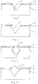
- FIGS. 1 to 11 each show a cross section through a silicon wafer 1, in particular a 4 ′′ wafer made of single-crystal silicon.
- the silicon wafer is provided with a mask, which is composed of a silicon oxide layer 3, for example 50 nm thick, and a silicon nitride layer, for example 140 nm thick.
- the surface of the silicon wafer 1 has masked and unmasked areas 4. If anisotropically etched such a masked silicon wafer 1 with a highly concentrated potassium hydroxide solution, V-shaped grooves 5 are formed in cross section in unmasked area 4 to modify the cross-sectionally V-shaped groove by repeated etching.
- the result is a groove with a diamond cross section 7, the geometry of which can be predetermined by the depth of the saw cut. ( Figures 1 to 4).
- the saw cutting depth and the sawing position must be observed very precisely and can be set, for example, with a precision saw.
- the precision saw used must be suitable for silicon materials. For example, a 40 ⁇ m thick diamond saw blade can be used. If you change the position of the saw cut, the cross section of the groove also changes.
- FIGS. 5 and 6 show a changed position of a saw cut 8 and the groove 9 formed after anisotropic etching.
- the saw cut and the groove symmetry axis do not match.
- the surface of the silicon wafer 1 corresponds to a (100) plane and the bounding edges correspond to the (111) planes which are inclined at 54.7 ° to the (100) plane and are distinguished by the fact that the etching rate perpendicular to these planes is very low compared to the etching rate perpendicular to other crystal planes.
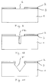
- FIG. 4 shows how an optical waveguide 10, a fiber, can be fixed in the modified groove with a diamond-shaped cross section.
- the groove should be a few centimeters long.
- the fixing properties of such a groove shape are improved compared to that of FIG. 2 by the elimination of a degree of freedom in the vertical direction to the fiber longitudinal axis. It is necessary that the groove cross section does not change over the entire area.
- FIG. 8 shows a movable slide made of silicon 11, on which, for example, an active optical component is mounted, which is movably inserted into a groove.
- Such an arrangement can serve, for example, as an optical switch in an electro-optical module.
- FIGS. 9 to 11 it is assumed that the masked silicon wafer is not etched in the first processing step, but is first provided with a saw cut 12.
- the saw cut is made in an unmasked area 4 of the surface of the silicon wafer 1.
- Anisotropic etching creates a groove 7 ', which then is diamond-shaped if the saw cut 12 has a corresponding saw cut depth.
Landscapes
- Engineering & Computer Science (AREA)
- Physics & Mathematics (AREA)
- General Physics & Mathematics (AREA)
- Computer Hardware Design (AREA)
- Condensed Matter Physics & Semiconductors (AREA)
- Manufacturing & Machinery (AREA)
- Microelectronics & Electronic Packaging (AREA)
- Power Engineering (AREA)
- Optics & Photonics (AREA)
- Chemical & Material Sciences (AREA)
- Chemical Kinetics & Catalysis (AREA)
- General Chemical & Material Sciences (AREA)
- Micromachines (AREA)
- Mechanical Coupling Of Light Guides (AREA)
Applications Claiming Priority (2)
| Application Number | Priority Date | Filing Date | Title |
|---|---|---|---|
| DE4213118 | 1992-04-21 | ||
| DE19924213118 DE4213118C1 (enExample) | 1992-04-21 | 1992-04-21 |
Publications (1)
| Publication Number | Publication Date |
|---|---|
| EP0566929A1 true EP0566929A1 (de) | 1993-10-27 |
Family
ID=6457170
Family Applications (1)
| Application Number | Title | Priority Date | Filing Date |
|---|---|---|---|
| EP93105737A Ceased EP0566929A1 (de) | 1992-04-21 | 1993-04-07 | Verfahren zum Herstellen von mikromechanischen Strukturen in einkristallinem Halbleitermaterial |
Country Status (2)
| Country | Link |
|---|---|
| EP (1) | EP0566929A1 (enExample) |
| DE (1) | DE4213118C1 (enExample) |
Cited By (3)
| Publication number | Priority date | Publication date | Assignee | Title |
|---|---|---|---|---|
| WO1995016192A1 (en) * | 1993-12-10 | 1995-06-15 | Pharmacia Biotech Ab | Method of producing cavity structures |
| WO1996034305A1 (en) * | 1995-04-27 | 1996-10-31 | Telefonaktiebolaget Lm Ericsson (Publ) | A silicon substrate having a recess for receiving an element, and a method of producing such a recess |
| DE19716480B4 (de) * | 1997-04-19 | 2004-03-25 | Micronas Semiconductor Holding Ag | Verfahren zum Herstellen einer Vorrichtung mit einem Hohlraum zur Aufnahme eines Lichtwellenleiters |
Families Citing this family (2)
| Publication number | Priority date | Publication date | Assignee | Title |
|---|---|---|---|---|
| GB2297626A (en) * | 1995-01-27 | 1996-08-07 | Cambridge Consultants | Miniature mounting grooved substrate |
| CN112397616A (zh) * | 2020-12-03 | 2021-02-23 | 宣城睿晖宣晟企业管理中心合伙企业(有限合伙) | 一种晶体硅电池片的切割方法及结构 |
Citations (3)
| Publication number | Priority date | Publication date | Assignee | Title |
|---|---|---|---|---|
| GB1246022A (en) * | 1968-09-14 | 1971-09-15 | Hitachi Ltd | Method of manufacturing semiconductor devices |
| US4522682A (en) * | 1982-06-21 | 1985-06-11 | Rockwell International Corporation | Method for producing PNP type lateral transistor separated from substrate by O.D.E. for minimal interference therefrom |
| US4604161A (en) * | 1985-05-02 | 1986-08-05 | Xerox Corporation | Method of fabricating image sensor arrays |
-
1992
- 1992-04-21 DE DE19924213118 patent/DE4213118C1/de not_active Expired - Fee Related
-
1993
- 1993-04-07 EP EP93105737A patent/EP0566929A1/de not_active Ceased
Patent Citations (3)
| Publication number | Priority date | Publication date | Assignee | Title |
|---|---|---|---|---|
| GB1246022A (en) * | 1968-09-14 | 1971-09-15 | Hitachi Ltd | Method of manufacturing semiconductor devices |
| US4522682A (en) * | 1982-06-21 | 1985-06-11 | Rockwell International Corporation | Method for producing PNP type lateral transistor separated from substrate by O.D.E. for minimal interference therefrom |
| US4604161A (en) * | 1985-05-02 | 1986-08-05 | Xerox Corporation | Method of fabricating image sensor arrays |
Non-Patent Citations (1)
| Title |
|---|
| PROCEEDINGS OF THE IEEE Bd. 70, Nr. 5, Mai 1982, NEW YORK US Seiten 420 - 457 K. E. PETERSEN 'Silicon as a mechanical material' paragraphs III and IV * |
Cited By (6)
| Publication number | Priority date | Publication date | Assignee | Title |
|---|---|---|---|---|
| WO1995016192A1 (en) * | 1993-12-10 | 1995-06-15 | Pharmacia Biotech Ab | Method of producing cavity structures |
| US5690841A (en) * | 1993-12-10 | 1997-11-25 | Pharmacia Biotech Ab | Method of producing cavity structures |
| WO1996034305A1 (en) * | 1995-04-27 | 1996-10-31 | Telefonaktiebolaget Lm Ericsson (Publ) | A silicon substrate having a recess for receiving an element, and a method of producing such a recess |
| US6100576A (en) * | 1995-04-27 | 2000-08-08 | Telefonaktiebolaget Lm Ericsson | Silicon substrate having a recess for receiving an element |
| US6482663B1 (en) | 1995-04-27 | 2002-11-19 | Telefonaktiebolaget Lm Ericsson (Publ) | Silicon substrate having a recess for receiving an element, and a method of producing such a recess |
| DE19716480B4 (de) * | 1997-04-19 | 2004-03-25 | Micronas Semiconductor Holding Ag | Verfahren zum Herstellen einer Vorrichtung mit einem Hohlraum zur Aufnahme eines Lichtwellenleiters |
Also Published As
| Publication number | Publication date |
|---|---|
| DE4213118C1 (enExample) | 1993-06-24 |
Similar Documents
| Publication | Publication Date | Title |
|---|---|---|
| DE69717635T2 (de) | Verfahren zur herstellung eines schneideinsatzes für schneidwerkzeug | |
| DE69204828T2 (de) | Herstellung von Laserdioden mit durch Spaltung erzeugten Stirnflächen auf einem vollständigen Wafer. | |
| DE69624099T2 (de) | Miniatur-haltevorrichtung | |
| DE3686923T2 (de) | Verfahren zur sichtbarkeitsverbesserung von ausrichtmarkierungen erster ordnung. | |
| EP0631159A1 (de) | Anordnung zur optischen Kopplung eines planaren optischen Wellenleiters und einer optischen Faser und Verfahren zur Herstellung eines für eine solche Anordnung geeigneten planaren Wellenleiters | |
| DE69711478T2 (de) | Herstellungsverfahren für III/V Halbleiterlaser | |
| EP0565999A2 (de) | Anordnung zur optischen Kopplung von zwei Gruppen von Wellenleitern | |
| DE69011751T2 (de) | Verfahren und Vorrichtung zur Markierung und Spaltung von monokristallinen halbleitenden Plättchen. | |
| EP0723670B9 (de) | Verfahren zur herstellung von prismen, insbesondere von mikroprismen und strahlungsteilern | |
| EP0012188A1 (de) | Verfahren zur Herstellung einer Lichtwellenleiterverzweigung | |
| EP0286855A1 (de) | Verfahren zum Aetzen von Vertiefungen in ein Siliziumsubstrat | |
| EP0711420B1 (de) | Verfahren zum herstellen eines silizium-halbleitersubstrats mit integriertem wellenleiter und daran angekoppelter optischer faser | |
| DE4213118C1 (enExample) | ||
| DE102014211555B4 (de) | Verfahren zum Ausbilden einer Kavität und Bauelement mit einer Kavität | |
| EP0509342B1 (de) | Verfahren zur Herstellung keilförmiger Strukturen | |
| DE4133885C2 (de) | Dreidimensionale Silizium-Struktur | |
| DE112018002065T5 (de) | Chip-herstellungsverfahren und siliziumchip | |
| DE19526711A1 (de) | Verfahren zur Bearbeitung von Siliciumwafern | |
| WO1999017349A1 (de) | Verfahren zur herstellung einer offenen dreidimensionalen microstruktur | |
| EP1042794A1 (de) | Verfahren zur herstellung einer porösen schicht mit hilfe eines elektrochemischen ätzprozesses | |
| EP0524179B1 (de) | Verfahren zum konfektionieren eines lichtwellenleiterschalters | |
| DE4133150A1 (de) | Verfahren zum abtrennen eines halbleiter-plaettchens aus einem halbleiter-plaettchenverband | |
| EP0798576A2 (de) | Optisches Bauelement mit Justiermarke und Verfahren zur Herstellung | |
| DE2358881C2 (de) | Verfahren zur Herstellung einer Ankopplungsoptik an einem Lichtwellenleiter | |
| DE4445835C2 (de) | Thermooptischer Schalter, insbesondere Richtkoppler, sowie Verfahren zu seiner Herstellung |
Legal Events
| Date | Code | Title | Description |
|---|---|---|---|
| PUAI | Public reference made under article 153(3) epc to a published international application that has entered the european phase |
Free format text: ORIGINAL CODE: 0009012 |
|
| 17P | Request for examination filed |
Effective date: 19930730 |
|
| AK | Designated contracting states |
Kind code of ref document: A1 Designated state(s): DE DK ES FR GB GR IT NL SE |
|
| 17Q | First examination report despatched |
Effective date: 19931201 |
|
| 18R | Application refused |
Effective date: 19951001 |