EP0566773A2 - Système de modulation en sauts de fréquence - Google Patents
Système de modulation en sauts de fréquence Download PDFInfo
- Publication number
- EP0566773A2 EP0566773A2 EP92111707A EP92111707A EP0566773A2 EP 0566773 A2 EP0566773 A2 EP 0566773A2 EP 92111707 A EP92111707 A EP 92111707A EP 92111707 A EP92111707 A EP 92111707A EP 0566773 A2 EP0566773 A2 EP 0566773A2
- Authority
- EP
- European Patent Office
- Prior art keywords
- data
- transmission
- pulse
- pulses
- signal
- Prior art date
- Legal status (The legal status is an assumption and is not a legal conclusion. Google has not performed a legal analysis and makes no representation as to the accuracy of the status listed.)
- Granted
Links
- 230000005540 biological transmission Effects 0.000 claims abstract description 53
- 238000000034 method Methods 0.000 claims abstract description 25
- 230000033228 biological regulation Effects 0.000 claims description 4
- 230000001360 synchronised effect Effects 0.000 claims description 4
- 101100295841 Arabidopsis thaliana OPT3 gene Proteins 0.000 claims description 3
- 230000008569 process Effects 0.000 claims description 2
- 230000001934 delay Effects 0.000 description 4
- 230000000630 rising effect Effects 0.000 description 3
- 238000011156 evaluation Methods 0.000 description 2
- 230000008929 regeneration Effects 0.000 description 2
- 238000011069 regeneration method Methods 0.000 description 2
- 230000007704 transition Effects 0.000 description 2
- 230000001960 triggered effect Effects 0.000 description 2
- 230000002457 bidirectional effect Effects 0.000 description 1
- 230000008859 change Effects 0.000 description 1
- 230000001419 dependent effect Effects 0.000 description 1
- 230000002349 favourable effect Effects 0.000 description 1
- 238000001914 filtration Methods 0.000 description 1
- 230000003287 optical effect Effects 0.000 description 1
- 230000010355 oscillation Effects 0.000 description 1
- 230000009467 reduction Effects 0.000 description 1
- 238000007493 shaping process Methods 0.000 description 1
- 238000001228 spectrum Methods 0.000 description 1
- 230000001629 suppression Effects 0.000 description 1
Images


Classifications
-
- H—ELECTRICITY
- H04—ELECTRIC COMMUNICATION TECHNIQUE
- H04L—TRANSMISSION OF DIGITAL INFORMATION, e.g. TELEGRAPHIC COMMUNICATION
- H04L27/00—Modulated-carrier systems
- H04L27/18—Phase-modulated carrier systems, i.e. using phase-shift keying
- H04L27/24—Half-wave signalling systems
Definitions
- the present invention relates to a method according to the preamble of claim 1 and a circuit arrangement for carrying out the method according to claims 6 and 7.
- Digital data which are to be transmitted from a transmitter to a receiver, are often converted in a first stage into a low-frequency signal, the frequency of which is changed or shifted between the values fh and ft (fh> ft) in accordance with the logical states of the input signal.
- This modulation method is known as "Frequency Shift Keying" (FSK).
- FSK Frequency Shift Keying
- the (FSK) modulated low-frequency signal is superimposed on a high-frequency carrier channel for the transmission of the digital data over longer electrical or optical lines or by means of directional radio.
- the radio frequency signal is demodulated at the receiving end.
- the (FSK) modulated low-frequency signal is recovered, which is demodulated in a discriminator stage.
- the final stage is usually the regeneration of the digital data.
- Such modulation and demodulation of the low-frequency signal which takes place in a modem, is known, for example, from P. Bocker, Data Transmission, Kunststoff 1976, Volume 2, pages 30-32.
- a frequency-keyed oscillator with an oscillating circuit is shown, the resonance frequency of which changes depending on the data to be transmitted.
- a demodulator with resonant circuit demodulator is shown, which regenerates the transmitted data signal.
- the course of the data occurring in the modem is shown on page 31, Figure 7.11.
- the frequency-modulated signal (2) has about 3.5 oscillations of the frequency fh or ft for a logic "1" of the transmission data and about 1.5 for a logic "0".
- the transmission or baud rate of the data signal is therefore approximately 3.5 times lower than the frequency fh.
- a high frequency fh leads to a correspondingly high bandwidth requirement when modulating a carrier channel.
- the transmission rate is therefore limited to a relatively low value given a fixed bandwidth.
- the transmission rate can be increased accordingly by reducing the vibrations per data bit.
- twice the bandwidth as for the data bits "0" is always required for the transmission of the data bits "1".
- the described method always results in a relatively low transmission rate in relation to the bandwidth required.
- the attenuation is often not constant over the frequency range of a transmission system and the phase is often not linearly increasing, so that signal deformations occur during transmission.
- group delays occur which lead to signal distortions, which normally leads to an increased error rate. With this method, signal distortions must therefore be reduced by means of complex equalization devices.
- DE-OS 2 008 897 also discloses a method for transmitting binary-coded data on a high-frequency channel, in which the binary coding is carried out by data-dependent keying of the carrier frequency.
- This method enables a transmission rate to be achieved which is significantly higher in the baseband range compared to the frequency shift keying described above.
- Radios in which the keying of the carrier frequency is provided allow the supply of a data signal to be transmitted in digital form. To carry out this hard frequency shift keying, however, special measures are necessary in the radio, which are not available in commercially available devices.
- the binary data signal is to be fed to the modulator via a DC voltage input, which is often not permitted in accordance with national regulations in order to keep the permitted frequency channels free of harmonics which would be supplied via such inputs and modulated onto the carrier channel.
- the present invention is therefore based on the object of providing a method and a circuit arrangement for carrying it out, by means of which data signals can be transmitted over an channel at an optimal transmission rate.
- the frequency of errors in data transmission is also to be reduced.
- data transmission should be possible via commercially available radio devices that can be used with little or no adjustments.
- the signal to be transmitted should be able to be fed to the radio via an AC voltage input.
- the method according to the invention achieves a transmission rate that is twice or four times as high as the frequency of the signal with which the carrier signal is modulated.
- the ratio of the transmission rate to the channel bandwidth is therefore optimal.
- the signal modulated with the binary data has only a single frequency, which eliminates distortions caused by group delays.
- the error rate is therefore reduced without having to use an equalizer as in the known methods.
- the method can also be used in conjunction with conventional radio equipment. Radios that have been in operation for a long time can be operated with the new method practically without additional measures.
- the transmission rate of these devices in use can be increased with a predetermined bandwidth and the error rate can be reduced.
- the transmission rate can be increased further (factor 4) with further measures and with a good signal-to-noise ratio.
- the circuit arrangement according to the invention enables the modulation and demodulation of a baseband signal, has a cost-effective structure and permits optimum shaping of the signals to be transmitted or optimal evaluation of the transmitted signals. Errors that have arisen in conventional discriminator stages, in particular as a result of interference signals, are largely eliminated.
- a baseband signal is again formed in accordance with the sequence "1101010011100" shown in FIG. 1a.
- a data bit "1" is assigned a positive or negative half-wave, for example with the frequency fh. It is provided that there is a change in polarity from half-wave to half-wave.
- the data bits "0” are assigned a DC voltage component of zero volts.
- pulses with a narrow-band frequency spectrum are often used instead of the half-waves shown, in which only "soft”"Transitions are provided.
- the bandwidth of the transmission channel can thus be restricted to a relatively small value without pulse deformations occurring.
- Cos2-shaped pulses are preferably selected which meet the requirements described.
- the transmission rate can be increased even further.
- Two half-waves or pulses of different amplitudes are provided, with which the baseband signal is modulated in accordance with the bit combinations "11", “10” and “0” or “11", “01” and “0".
- the bit combinations "11” and “10” or “11” and “01” are assigned the half-waves of different amplitudes and the bit "0” is assigned a signal component of zero volts and half the length of a half-wave.
- the data units "0" and “1” could also be interchanged.
- the combination "11” is assigned a half wave with an amplitude 1 and the combination "10" a half wave with the amplitude 0.5.
- a transmission rate that is twice as high as compared to the type of modulation shown in FIG. 1b and four times as high as compared to the type of modulation shown in FIG. 1a can be achieved.
- Appropriate decision thresholds or decision criteria must be provided for the signals of different amplitudes in the associated demodulation stage.
- FIG. 2a shows a circuit arrangement which is provided for the modulation and demodulation of a baseband signal.
- This modem is connected to a transmission line (not shown in FIG. 2) or to a radio device which, according to national regulations, normally has only one AC voltage input and output.
- a bidirectional data bus DB via a processor CPU, a digital / analog converter D / A, a bandpass filter BPS and an output transformer TFA with the input and via the processor CPU, a comparator COMP, another bandpass filter BPE and an input transformer TFE with connected to the output of the radio.
- Data arriving via the data bus DB are converted into sequences of data words by the processor CPU and applied to the converter D / A in such a way that a positive or negative half-wave alternates at the output of the converter D for each data bit “1” in accordance with the method described at the beginning / A is delivered.
- the generated analog signal is sent to the AC voltage input of the radio via the output transformer TFA, any harmonics are eliminated in the bandpass filter BPS in order to avoid interference with neighboring radio channels.
- a modulation of the carrier signal proportional to the input signal takes place in the radio.
- the comparator COMP therefore outputs a data bit "1" to the processor CPU.
- the processor CPU and the converter D / A can produce the desired pulse shapes only in a relatively rough approximation, which, for example, can result in insufficient suppression of inter-symbol interference.
- the data bus DB is therefore via a signal processor DSP, a counter CTRS, a pulse width modulator PWMS, an optocoupler OPT1 and a pulse width demodulator PWD with the input and via the signal processor DSP, another counter CTRE, another optocoupler OPT2 and another Pulse width modulator PWME connected to the output of the radio.
- the pulse width modulator PWME is connected to a control unit CL via a further optocoupler OPT3, the signal processor DSP and the counter units CTR.
- the digital signal processor DSP has an expanded bus structure compared to conventional processors, which means that various operations (calculations, reads and saves) can be carried out simultaneously. Such processors DSP, which have an extremely high working speed, are particularly well suited for signal processing.
- the start and stop signals that determine the pulse width or only the stop signals can be output from the counter CTRS to the modulator PWMS.
- the counter CTRS has to be synchronized with a reference frequency; otherwise the counter CTRS and the modulator PWMS are to be clocked periodically, for example by the control unit CL.
- the modulated square-wave signal or the modulated pulses are subsequently output via the optocoupler OPT1 to the demodulator PWD, which converts the pulses into an analog signal.
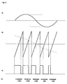
- Fig. 3d are the 8-bit data words output by the signal processor DSP which determines how high the counter should run and which, as is known, can take decimal values between 0 and 256.
- the counter CTRS which (with 8-bit words) can count up to a maximum of 256 within the period of the square wave signal, counts up to the counter reading specified by the data word.
- the time consumed in this case corresponds exactly to the pulse duration ti, as a result of which the width of the pulses shown in FIG. 3c is determined.
- the square-wave signals are filtered via a filter (low-pass filter of the n-th order), which produces the analog signal shown in FIG. 3a, which is emitted by the demodulator PWD to the radio.
- the signal processor DSP can be used to form any pulse shape by means of which a low inter-symbol interference can be achieved.
- a sequence of 8-bit data words corresponding to the desired pulse shape is therefore stored in the signal processor DSP and is read out as soon as a data bit "1" to be transmitted occurs.
- Values from 128 to 256 are provided for positive pulses (for 8-bit data words) and values from 0 to 128 for the data words for negative pulses.
- the width of the impulses is therefore determined in the transmission path depending on the data words present.
- the pulse width is determined in the reception path as a function of an analog signal emitted by the radio.
- the respective pulse width ti of the rectangular pulses is determined by comparing the sawtooth voltage shown in FIG. 3b with the analog signal supplied to the demodulator PWME by the radio. The intersection of both signals results in the falling edge of the modulated pulses.
- the rising edges of both signals (sawtooth and square wave signal) and the start of the start or trigger signal for the downstream counter CTRE are again synchronized. When the rising edge of the rectangular pulse occurs, the counter CTRE begins to count and is stopped by the falling edge of the rectangular signal after the pulse duration ti has elapsed.
- the counted value which (in the case of 8-bit data words) is again between 0 and 256, is subsequently transferred from the counter CTRE to the signal processor DSP.
- a pulse received by the radio is therefore converted into a sequence of 8-bit data words by the receiving circuit described and fed to the signal processor DSP, which can process and evaluate the received data words.
- Extreme changes in individual pulse widths or corresponding data words caused by disturbances can be averaged out and corrected. That is, spikes that would be converted into data bits "1" in the comparator circuit COMP according to FIG. 2a normally only falsify a pulse from the entire sequence in the circuits according to FIGS. 2b and 2c that can be easily corrected.
- the error rate can therefore be significantly reduced with these circuits. This enables data transmission over longer distances or even under less favorable conditions.
- the optocouplers OPT1, OPT2 and OPT3 decouple the input and output of the modem in terms of DC voltage.
- the counters CTRS and CTRE could at best be replaced by a single counter operating in time-division multiplex mode. There is also the possibility of integrating the functions of the counters CTRS, CTRE and the pulse width modulation stage PWMS in the processor DSP.
- the line shown in dashed lines in FIG. 2b indicates that the modules CL, CTRE, CTRS and PWMS contained therein can also be implemented in software.
- the circuit arrangement according to FIG. 2c has the same function as the circuit arrangement according to FIG. 2b.
- the DC decoupling of the input and output of the modem is carried out via two transformers TFE and TFA.
- the regeneration of a signal clock with which a sequence of signal samples or of data words to be transferred to the signal processor is triggered is possible in various ways. It is advantageous to send fewer synchronization pulses, by means of which a clock generator, which is preferably provided in the control unit CL, is triggered. To prevent the clock pulses of the generator and the transmitted signals from diverging, it is provided that the clock generator is restarted with each pulse received. So that the divergence of the clocks is also prevented if a longer series of data bits "0" is transmitted, e.g. a sync pulse is inserted after every nth data bit.
Landscapes
- Engineering & Computer Science (AREA)
- Computer Networks & Wireless Communication (AREA)
- Signal Processing (AREA)
- Digital Transmission Methods That Use Modulated Carrier Waves (AREA)
- Dc Digital Transmission (AREA)
- Communication Control (AREA)
Applications Claiming Priority (3)
| Application Number | Priority Date | Filing Date | Title |
|---|---|---|---|
| CH131592 | 1992-04-23 | ||
| CH1315/92 | 1992-04-23 | ||
| CH1315/92A CH684860A5 (de) | 1992-04-23 | 1992-04-23 | Verfahren und Schaltungsanordnung zur Uebertragung von binären Datenfolgen. |
Publications (3)
| Publication Number | Publication Date |
|---|---|
| EP0566773A2 true EP0566773A2 (fr) | 1993-10-27 |
| EP0566773A3 EP0566773A3 (fr) | 1994-01-12 |
| EP0566773B1 EP0566773B1 (fr) | 2000-03-08 |
Family
ID=4207573
Family Applications (1)
| Application Number | Title | Priority Date | Filing Date |
|---|---|---|---|
| EP92111707A Expired - Lifetime EP0566773B1 (fr) | 1992-04-23 | 1992-07-09 | Procédé et dispositif pour la transmission de données binaires |
Country Status (6)
| Country | Link |
|---|---|
| US (1) | US5623518A (fr) |
| EP (1) | EP0566773B1 (fr) |
| AT (1) | ATE190447T1 (fr) |
| CH (1) | CH684860A5 (fr) |
| DE (1) | DE59209817D1 (fr) |
| ES (1) | ES2142806T3 (fr) |
Families Citing this family (27)
| Publication number | Priority date | Publication date | Assignee | Title |
|---|---|---|---|---|
| TW256900B (fr) * | 1993-11-25 | 1995-09-11 | Alps Electric Co Ltd | |
| FR2719175B1 (fr) * | 1994-04-20 | 1996-05-31 | Cit Alcatel | Procédé de transmission optique présentant une sensibilité réduite à la dispersion, et système de transmission pour la mise en Óoeuvre de ce procédé. |
| JP2968706B2 (ja) * | 1995-07-26 | 1999-11-02 | 日本電気エンジニアリング株式会社 | 移動無線機 |
| US5748902A (en) * | 1996-07-19 | 1998-05-05 | Compaq Computer Corporation | Polarity switched data bus for reduced electromagnetic interference |
| US6351489B1 (en) * | 1996-09-30 | 2002-02-26 | Rosemount Inc. | Data bus communication technique for field instrument |
| DE19716323A1 (de) * | 1997-04-18 | 1998-10-22 | Alsthom Cge Alcatel | Modulationseinrichtung zur Modulation digitaler Signale |
| US6002279A (en) * | 1997-10-24 | 1999-12-14 | G2 Networks, Inc. | Clock recovery circuit |
| US6104732A (en) * | 1997-10-24 | 2000-08-15 | G-2 Networks, Inc. | Integrated signal routing circuit |
| US6577687B2 (en) | 1998-12-23 | 2003-06-10 | Maxtor Corporation | Method for transmitting data over a data bus with minimized digital inter-symbol interference |
| US6188314B1 (en) | 1999-02-03 | 2001-02-13 | Trw Inc. | Energy distribution and communication system and method utilizing a communication message frame for a multi-device vehicle occupant protection system |
| US6044113A (en) * | 1999-02-17 | 2000-03-28 | Visx, Inc. | Digital pulse width modulator |
| US6697375B1 (en) * | 1999-08-04 | 2004-02-24 | Atheros Communications, Inc. | Method and apparatus for bandwidth and frequency management in the U-NII band |
| US7095796B1 (en) * | 2002-01-07 | 2006-08-22 | Vixs, Inc. | Low power radio transmitter using pulse transmissions |
| US7127017B1 (en) | 2002-07-19 | 2006-10-24 | Rambus, Inc. | Clock recovery circuit with second order digital filter |
| US7158594B2 (en) * | 2002-08-21 | 2007-01-02 | Intel Corporation | Receivers for controlled frequency signals |
| US7224739B2 (en) * | 2002-08-21 | 2007-05-29 | Intel Corporation | Controlled frequency signals |
| US6836226B2 (en) * | 2002-11-12 | 2004-12-28 | Pulse-Link, Inc. | Ultra-wideband pulse modulation system and method |
| WO2004102818A2 (fr) * | 2003-01-27 | 2004-11-25 | Xg Technology, Llc | Modulation a sauts de frequence par cycles entiers pour l'emission hertzienne de donnees a grande vitesse |
| CA2531009C (fr) * | 2003-06-24 | 2014-10-28 | Xg Technology, Llc | Modulation de cycle de nombre entier a trois etats |
| US7305023B2 (en) * | 2003-07-23 | 2007-12-04 | Intel Corporation | Receivers for cycle encoded signals |
| US7308025B2 (en) * | 2003-07-23 | 2007-12-11 | Intel Corporation | Transmitters providing cycle encoded signals |
| US7126435B2 (en) * | 2003-09-23 | 2006-10-24 | Rambus Inc. | Voltage controlled oscillator amplitude control circuit |
| US20050271150A1 (en) * | 2004-06-07 | 2005-12-08 | Steve Moore | Digital modulation system and method |
| US7864889B2 (en) * | 2004-06-15 | 2011-01-04 | Robert Bosch Gmbh | Method and system for establishing an adaptable offset for a receiver |
| JP2006211451A (ja) * | 2005-01-31 | 2006-08-10 | General Res Of Electronics Inc | Fsk信号発生回路 |
| US8774291B2 (en) * | 2009-12-09 | 2014-07-08 | Georgia Tech Research Corporation | Pulse harmonic modulation systems and methods |
| US8894020B2 (en) * | 2011-02-28 | 2014-11-25 | Harvey J. Rosener | Block module for model train layout control |
Citations (5)
| Publication number | Priority date | Publication date | Assignee | Title |
|---|---|---|---|---|
| US3560856A (en) * | 1966-12-29 | 1971-02-02 | Nippon Electric Co | Multilevel signal transmission system |
| DE3133397A1 (de) * | 1981-08-24 | 1983-03-31 | Josef Ing.(grad.) 8000 München Dirr | Verfahren fuer das digitale bildfernsprechen |
| US4417349A (en) * | 1979-11-08 | 1983-11-22 | Digital Broadcasting Corporation | SCA Data transmission system with a raised cosine filter |
| EP0344615A2 (fr) * | 1988-06-03 | 1989-12-06 | National Semiconductor Corporation | Emetteur numérique pour signaux codés en 2B1Q à grande précision et à réponse linéaire dans le domaine temporel |
| WO1991002403A1 (fr) * | 1989-08-07 | 1991-02-21 | Motorola, Inc. | Systeme de modulation fm numerique a efficacite spectrale |
Family Cites Families (17)
| Publication number | Priority date | Publication date | Assignee | Title |
|---|---|---|---|---|
| US3697874A (en) * | 1966-12-29 | 1972-10-10 | Nippon Electric Co | Multilevel code conversion system |
| DE2008897A1 (fr) * | 1970-02-26 | 1971-09-02 | Bosch Elektronik Gmbh | |
| US4357634A (en) * | 1979-10-01 | 1982-11-02 | Chung David H | Encoding and decoding digital information utilizing time intervals between pulses |
| US4425665A (en) * | 1981-09-24 | 1984-01-10 | Advanced Micro Devices, Inc. | FSK Voiceband modem using digital filters |
| US4489222A (en) * | 1982-09-13 | 1984-12-18 | The Board Of Trustees Of The Leland Stanford, Junior University | Telephone line interface |
| US4627078A (en) * | 1983-08-25 | 1986-12-02 | The Microperipheral Corporation | Data communication system |
| US4689801A (en) * | 1983-10-11 | 1987-08-25 | American Standard Inc. | Microprocessor FSK data communications module |
| US4644561A (en) * | 1985-03-20 | 1987-02-17 | International Mobile Machines Corp. | Modem for RF subscriber telephone system |
| US5185765A (en) * | 1986-05-08 | 1993-02-09 | Walker Harold R | High speed data communication system using phase shift key coding |
| US4871987A (en) * | 1987-03-28 | 1989-10-03 | Kabushiki Kaisha Kenwood | FSK or am modulator with digital waveform shaping |
| US4926444A (en) * | 1988-04-29 | 1990-05-15 | Scientific-Atlanta, Inc. | Data transmission method and apparatus by period shift keying (TSK) |
| US5132957A (en) * | 1988-11-07 | 1992-07-21 | Teac Corporation | Information signal recording and reproducing system capable of recording an information signal on a medium having a limited recording band width |
| US5237590A (en) * | 1989-03-13 | 1993-08-17 | Hitachi, Ltd. | Timing extraction circuit and communication system utilizing the same |
| US5202900A (en) * | 1989-08-07 | 1993-04-13 | Motorola, Inc. | Spectrally efficient digital FM modulated transmitter |
| US5103463A (en) * | 1990-08-30 | 1992-04-07 | Comacs, Ltd. | Method and system for encoding and decoding frequency shift keying signals |
| US5227741A (en) * | 1992-01-22 | 1993-07-13 | Glenayre Electronics Ltd. | Variable speed asynchronous modem |
| US5406584A (en) * | 1992-09-01 | 1995-04-11 | X-Com, Inc. | Time shift keying digital communications system |
-
1992
- 1992-04-23 CH CH1315/92A patent/CH684860A5/de not_active IP Right Cessation
- 1992-07-09 AT AT92111707T patent/ATE190447T1/de not_active IP Right Cessation
- 1992-07-09 ES ES92111707T patent/ES2142806T3/es not_active Expired - Lifetime
- 1992-07-09 DE DE59209817T patent/DE59209817D1/de not_active Expired - Fee Related
- 1992-07-09 EP EP92111707A patent/EP0566773B1/fr not_active Expired - Lifetime
-
1993
- 1993-04-16 US US08/047,193 patent/US5623518A/en not_active Expired - Lifetime
Patent Citations (5)
| Publication number | Priority date | Publication date | Assignee | Title |
|---|---|---|---|---|
| US3560856A (en) * | 1966-12-29 | 1971-02-02 | Nippon Electric Co | Multilevel signal transmission system |
| US4417349A (en) * | 1979-11-08 | 1983-11-22 | Digital Broadcasting Corporation | SCA Data transmission system with a raised cosine filter |
| DE3133397A1 (de) * | 1981-08-24 | 1983-03-31 | Josef Ing.(grad.) 8000 München Dirr | Verfahren fuer das digitale bildfernsprechen |
| EP0344615A2 (fr) * | 1988-06-03 | 1989-12-06 | National Semiconductor Corporation | Emetteur numérique pour signaux codés en 2B1Q à grande précision et à réponse linéaire dans le domaine temporel |
| WO1991002403A1 (fr) * | 1989-08-07 | 1991-02-21 | Motorola, Inc. | Systeme de modulation fm numerique a efficacite spectrale |
Non-Patent Citations (2)
| Title |
|---|
| IEEE JOURNAL OF SOLID-STATE CIRCUITS Bd. 24, Nr. 6 , Dezember 1989 , NEW YORK US Seiten 1614 - 1623 XP100493 R. P. COLBECK ET AL.: 'A Single-Chip 2B1Q U-Interface Transceiver.' * |
| International Telecommunications Symposium ITS '90, Rio de Janeiro, BR, 03.- 06.09.1990, pages 525-528, IEEE, New York, US; XP245474; J. A. DELGADO-PENIN / A. CORREAS-CORCOBADO: 'Power Spectral Density of a novel Adaptive Multilevel Line Code.' * |
Also Published As
| Publication number | Publication date |
|---|---|
| ES2142806T3 (es) | 2000-05-01 |
| EP0566773A3 (fr) | 1994-01-12 |
| ATE190447T1 (de) | 2000-03-15 |
| CH684860A5 (de) | 1995-01-13 |
| EP0566773B1 (fr) | 2000-03-08 |
| US5623518A (en) | 1997-04-22 |
| DE59209817D1 (de) | 2000-04-13 |
Similar Documents
| Publication | Publication Date | Title |
|---|---|---|
| EP0566773B1 (fr) | Procédé et dispositif pour la transmission de données binaires | |
| DE69429779T2 (de) | Digitale kommunikationseinrichtung unter verwendung einer vierfachen differenzfrequenzumtastung | |
| DE69534625T2 (de) | Mehrschwellendetektion für 0.3-GMSK | |
| DE69313802T2 (de) | Empfangsgerät für ein bandgespreiztes Signal | |
| DE2045794A1 (de) | Datendemodulator mit Verwendung von Vergleichen | |
| DE10301637A1 (de) | Sende-/Empfangseinrichtung für eine an ein Kommunikations-Netzwerk angeschlossene Komponente eines Kraftfahrzeugs | |
| DE2245189B2 (de) | Vorrichtung zur Übertragung eines restseitenbandträgermodulierten Mehrpegelsignals und eines Synchronisier-Pilotsignals | |
| EP1051816A1 (fr) | Dispositif pour la transmission de signaux avec un faible niveau de brouillage | |
| DE69527937T2 (de) | Empfänger mit einstellbarem symbolentscheider | |
| DE2101076A1 (de) | Digitales Datenubertragungssystem rmt hoher Arbeitsgeschwindigkeit | |
| AT401838B (de) | Verfahren zur aufbereitung von signalen für die signalübertragung im basisband | |
| EP1419583A1 (fr) | Procede de filtrage adaptatif et filtres permettant de filtrer un signal radio dans un systeme de communication radiomobile | |
| DE2155958B2 (de) | Schaltungsanordnung zur Ent zerrung eines Signals | |
| EP1490962B1 (fr) | Demodulation d'un signal de reception analogique module en frequence numeriquement par evaluation des ecarts temporels entre les passages par zero | |
| DE10157392C2 (de) | Empfänger mit Offsetkompensation | |
| EP0797334B1 (fr) | Transmission de données en employant simultanément MDF et MDA | |
| DE1591810A1 (de) | Nachrichtenuebertragungssystem mit differentieller Phasenmodulation | |
| DE3730399A1 (de) | Verfahren und vorrichtung zur uebertragung eines digitalsignals | |
| DE69015041T2 (de) | Einrichtung zur Korrektur der Übertragungsverzerrungen eines Datensignals in Abhängigkeit von Übertragungskodeverletzungen. | |
| EP1018221B1 (fr) | Procede et circuit pour la transmission de messages en utilisant des approximations de fonctions hermitiennes | |
| DE3010537A1 (de) | Anordnung zur uebertragung digitaler daten | |
| DE4402512C1 (de) | Verfahren zur schnellen und störsicheren Übertragung von Nutzdaten zwischen zwei Datenpumpen | |
| DE4136205C1 (en) | Signal processing circuit for cordless telephone - reduces signal harmonics in data transmission using Manchester decoder to extract information from received triangular signal | |
| DE3245244C1 (de) | Methode zur simultanen Übertragung von binären Daten und Telefonsprechsignalen innerhalb des Sprachbandes eines Telefon-Übertragungskanals | |
| EP0093819A1 (fr) | Système pour la transmission radiophonique d'un signal en code binaire |
Legal Events
| Date | Code | Title | Description |
|---|---|---|---|
| PUAI | Public reference made under article 153(3) epc to a published international application that has entered the european phase |
Free format text: ORIGINAL CODE: 0009012 |
|
| 17P | Request for examination filed |
Effective date: 19930112 |
|
| AK | Designated contracting states |
Kind code of ref document: A2 Designated state(s): AT BE CH DE ES FR GB IT LI NL PT SE |
|
| PUAL | Search report despatched |
Free format text: ORIGINAL CODE: 0009013 |
|
| AK | Designated contracting states |
Kind code of ref document: A3 Designated state(s): AT BE CH DE ES FR GB IT LI NL PT SE |
|
| RHK1 | Main classification (correction) |
Ipc: H04L 27/24 |
|
| 17Q | First examination report despatched |
Effective date: 19961025 |
|
| GRAG | Despatch of communication of intention to grant |
Free format text: ORIGINAL CODE: EPIDOS AGRA |
|
| GRAG | Despatch of communication of intention to grant |
Free format text: ORIGINAL CODE: EPIDOS AGRA |
|
| GRAH | Despatch of communication of intention to grant a patent |
Free format text: ORIGINAL CODE: EPIDOS IGRA |
|
| GRAH | Despatch of communication of intention to grant a patent |
Free format text: ORIGINAL CODE: EPIDOS IGRA |
|
| GRAA | (expected) grant |
Free format text: ORIGINAL CODE: 0009210 |
|
| STAA | Information on the status of an ep patent application or granted ep patent |
Free format text: STATUS: THE PATENT HAS BEEN GRANTED |
|
| AK | Designated contracting states |
Kind code of ref document: B1 Designated state(s): AT BE CH DE ES FR GB IT LI NL PT SE |
|
| PG25 | Lapsed in a contracting state [announced via postgrant information from national office to epo] |
Ref country code: SE Free format text: THE PATENT HAS BEEN ANNULLED BY A DECISION OF A NATIONAL AUTHORITY Effective date: 20000308 |
|
| REF | Corresponds to: |
Ref document number: 190447 Country of ref document: AT Date of ref document: 20000315 Kind code of ref document: T |
|
| REG | Reference to a national code |
Ref country code: CH Ref legal event code: EP |
|
| REF | Corresponds to: |
Ref document number: 59209817 Country of ref document: DE Date of ref document: 20000413 |
|
| REG | Reference to a national code |
Ref country code: ES Ref legal event code: FG2A Ref document number: 2142806 Country of ref document: ES Kind code of ref document: T3 |
|
| GBT | Gb: translation of ep patent filed (gb section 77(6)(a)/1977) |
Effective date: 20000413 |
|
| ITF | It: translation for a ep patent filed | ||
| PG25 | Lapsed in a contracting state [announced via postgrant information from national office to epo] |
Ref country code: PT Free format text: LAPSE BECAUSE OF FAILURE TO SUBMIT A TRANSLATION OF THE DESCRIPTION OR TO PAY THE FEE WITHIN THE PRESCRIBED TIME-LIMIT Effective date: 20000608 |
|
| ET | Fr: translation filed | ||
| PLBE | No opposition filed within time limit |
Free format text: ORIGINAL CODE: 0009261 |
|
| 26N | No opposition filed | ||
| REG | Reference to a national code |
Ref country code: GB Ref legal event code: IF02 |
|
| REG | Reference to a national code |
Ref country code: CH Ref legal event code: PFA Free format text: HAENI PROLECTRON AG TRANSFER- SIEMENS TRANSIT TELEMATIC SYSTEMS AG Ref country code: CH Ref legal event code: NV Representative=s name: SIEMENS SCHWEIZ AG |
|
| NLT1 | Nl: modifications of names registered in virtue of documents presented to the patent office pursuant to art. 16 a, paragraph 1 |
Owner name: SIEMENS TRANSIT TELEMATICS SYSTEMS AG |
|
| REG | Reference to a national code |
Ref country code: ES Ref legal event code: PC2A |
|
| PGFP | Annual fee paid to national office [announced via postgrant information from national office to epo] |
Ref country code: NL Payment date: 20030708 Year of fee payment: 12 |
|
| PGFP | Annual fee paid to national office [announced via postgrant information from national office to epo] |
Ref country code: ES Payment date: 20030730 Year of fee payment: 12 |
|
| REG | Reference to a national code |
Ref country code: FR Ref legal event code: CD |
|
| PG25 | Lapsed in a contracting state [announced via postgrant information from national office to epo] |
Ref country code: ES Free format text: LAPSE BECAUSE OF NON-PAYMENT OF DUE FEES Effective date: 20040710 |
|
| PGFP | Annual fee paid to national office [announced via postgrant information from national office to epo] |
Ref country code: BE Payment date: 20040713 Year of fee payment: 13 |
|
| PGFP | Annual fee paid to national office [announced via postgrant information from national office to epo] |
Ref country code: FR Payment date: 20040716 Year of fee payment: 13 |
|
| PG25 | Lapsed in a contracting state [announced via postgrant information from national office to epo] |
Ref country code: NL Free format text: LAPSE BECAUSE OF NON-PAYMENT OF DUE FEES Effective date: 20050201 |
|
| NLV4 | Nl: lapsed or anulled due to non-payment of the annual fee |
Effective date: 20050201 |
|
| PG25 | Lapsed in a contracting state [announced via postgrant information from national office to epo] |
Ref country code: IT Free format text: LAPSE BECAUSE OF NON-PAYMENT OF DUE FEES;WARNING: LAPSES OF ITALIAN PATENTS WITH EFFECTIVE DATE BEFORE 2007 MAY HAVE OCCURRED AT ANY TIME BEFORE 2007. THE CORRECT EFFECTIVE DATE MAY BE DIFFERENT FROM THE ONE RECORDED. Effective date: 20050709 |
|
| PG25 | Lapsed in a contracting state [announced via postgrant information from national office to epo] |
Ref country code: BE Free format text: LAPSE BECAUSE OF NON-PAYMENT OF DUE FEES Effective date: 20050731 |
|
| REG | Reference to a national code |
Ref country code: CH Ref legal event code: PFA Owner name: SIEMENS VDO AUTOMOTIVE AG Free format text: SIEMENS TRANSIT TELEMATIC SYSTEMS AG#INDUSTRIESTRASSE 4#9552 BRONSCHHOFEN (CH) -TRANSFER TO- SIEMENS VDO AUTOMOTIVE AG#INDUSTRIEPLATZ 3#8212 NEUHAUSEN AM RHEINFALL (CH) |
|
| REG | Reference to a national code |
Ref country code: ES Ref legal event code: FD2A Effective date: 20040710 |
|
| REG | Reference to a national code |
Ref country code: GB Ref legal event code: 732E |
|
| PG25 | Lapsed in a contracting state [announced via postgrant information from national office to epo] |
Ref country code: FR Free format text: LAPSE BECAUSE OF NON-PAYMENT OF DUE FEES Effective date: 20060331 |
|
| REG | Reference to a national code |
Ref country code: FR Ref legal event code: ST Effective date: 20060331 |
|
| BERE | Be: lapsed |
Owner name: *SIEMENS TRANSIT TELEMATIC SYSTEMS A.G. Effective date: 20050731 |
|
| REG | Reference to a national code |
Ref country code: CH Ref legal event code: PFA Owner name: CONTINENTAL AUTOMOTIVE SWITZERLAND AG Free format text: SIEMENS VDO AUTOMOTIVE AG#INDUSTRIEPLATZ 3#8212 NEUHAUSEN AM RHEINFALL (CH) -TRANSFER TO- CONTINENTAL AUTOMOTIVE SWITZERLAND AG#INDUSTRIEPLATZ 3#8212 NEUHAUSEN AM RHEINFALL (CH) |
|
| REG | Reference to a national code |
Ref country code: CH Ref legal event code: PCAR Free format text: SIEMENS SCHWEIZ AG;INTELLECTUAL PROPERTY FREILAGERSTRASSE 40;8047 ZUERICH (CH) |
|
| PGFP | Annual fee paid to national office [announced via postgrant information from national office to epo] |
Ref country code: DE Payment date: 20090731 Year of fee payment: 18 |
|
| PGFP | Annual fee paid to national office [announced via postgrant information from national office to epo] |
Ref country code: CH Payment date: 20100726 Year of fee payment: 19 |
|
| PGFP | Annual fee paid to national office [announced via postgrant information from national office to epo] |
Ref country code: AT Payment date: 20100714 Year of fee payment: 19 |
|
| PGFP | Annual fee paid to national office [announced via postgrant information from national office to epo] |
Ref country code: GB Payment date: 20100722 Year of fee payment: 19 |
|
| PG25 | Lapsed in a contracting state [announced via postgrant information from national office to epo] |
Ref country code: DE Free format text: LAPSE BECAUSE OF NON-PAYMENT OF DUE FEES Effective date: 20110201 |
|
| REG | Reference to a national code |
Ref country code: DE Ref legal event code: R119 Ref document number: 59209817 Country of ref document: DE Effective date: 20110201 |
|
| REG | Reference to a national code |
Ref country code: CH Ref legal event code: PL |
|
| GBPC | Gb: european patent ceased through non-payment of renewal fee |
Effective date: 20110709 |
|
| REG | Reference to a national code |
Ref country code: AT Ref legal event code: MM01 Ref document number: 190447 Country of ref document: AT Kind code of ref document: T Effective date: 20110709 |
|
| PG25 | Lapsed in a contracting state [announced via postgrant information from national office to epo] |
Ref country code: LI Free format text: LAPSE BECAUSE OF NON-PAYMENT OF DUE FEES Effective date: 20110731 Ref country code: CH Free format text: LAPSE BECAUSE OF NON-PAYMENT OF DUE FEES Effective date: 20110731 |
|
| PG25 | Lapsed in a contracting state [announced via postgrant information from national office to epo] |
Ref country code: GB Free format text: LAPSE BECAUSE OF NON-PAYMENT OF DUE FEES Effective date: 20110709 |
|
| PG25 | Lapsed in a contracting state [announced via postgrant information from national office to epo] |
Ref country code: AT Free format text: LAPSE BECAUSE OF NON-PAYMENT OF DUE FEES Effective date: 20110709 |