EP0565054A2 - N-typ-Antimonbasis-Übergitterstruktur mit Spannungsschicht und Verfahren zur Herstellung - Google Patents
N-typ-Antimonbasis-Übergitterstruktur mit Spannungsschicht und Verfahren zur Herstellung Download PDFInfo
- Publication number
- EP0565054A2 EP0565054A2 EP93105687A EP93105687A EP0565054A2 EP 0565054 A2 EP0565054 A2 EP 0565054A2 EP 93105687 A EP93105687 A EP 93105687A EP 93105687 A EP93105687 A EP 93105687A EP 0565054 A2 EP0565054 A2 EP 0565054A2
- Authority
- EP
- European Patent Office
- Prior art keywords
- layer
- layers
- base
- strained
- compound
- Prior art date
- Legal status (The legal status is an assumption and is not a legal conclusion. Google has not performed a legal analysis and makes no representation as to the accuracy of the status listed.)
- Withdrawn
Links
Images
Classifications
-
- H—ELECTRICITY
- H10—SEMICONDUCTOR DEVICES; ELECTRIC SOLID-STATE DEVICES NOT OTHERWISE PROVIDED FOR
- H10D—INORGANIC ELECTRIC SEMICONDUCTOR DEVICES
- H10D62/00—Semiconductor bodies, or regions thereof, of devices having potential barriers
- H10D62/10—Shapes, relative sizes or dispositions of the regions of the semiconductor bodies; Shapes of the semiconductor bodies
- H10D62/13—Semiconductor regions connected to electrodes carrying current to be rectified, amplified or switched, e.g. source or drain regions
- H10D62/149—Source or drain regions of field-effect devices
- H10D62/151—Source or drain regions of field-effect devices of IGFETs
-
- H—ELECTRICITY
- H10—SEMICONDUCTOR DEVICES; ELECTRIC SOLID-STATE DEVICES NOT OTHERWISE PROVIDED FOR
- H10D—INORGANIC ELECTRIC SEMICONDUCTOR DEVICES
- H10D30/00—Field-effect transistors [FET]
- H10D30/01—Manufacture or treatment
- H10D30/015—Manufacture or treatment of FETs having heterojunction interface channels or heterojunction gate electrodes, e.g. HEMT
-
- H—ELECTRICITY
- H10—SEMICONDUCTOR DEVICES; ELECTRIC SOLID-STATE DEVICES NOT OTHERWISE PROVIDED FOR
- H10D—INORGANIC ELECTRIC SEMICONDUCTOR DEVICES
- H10D30/00—Field-effect transistors [FET]
- H10D30/40—FETs having zero-dimensional [0D], one-dimensional [1D] or two-dimensional [2D] charge carrier gas channels
- H10D30/47—FETs having zero-dimensional [0D], one-dimensional [1D] or two-dimensional [2D] charge carrier gas channels having two-dimensional [2D] charge carrier gas channels, e.g. nanoribbon FETs or high electron mobility transistors [HEMT]
- H10D30/471—High electron mobility transistors [HEMT] or high hole mobility transistors [HHMT]
- H10D30/473—High electron mobility transistors [HEMT] or high hole mobility transistors [HHMT] having confinement of carriers by multiple heterojunctions, e.g. quantum well HEMT
- H10D30/4732—High electron mobility transistors [HEMT] or high hole mobility transistors [HHMT] having confinement of carriers by multiple heterojunctions, e.g. quantum well HEMT using Group III-V semiconductor material
-
- H—ELECTRICITY
- H10—SEMICONDUCTOR DEVICES; ELECTRIC SOLID-STATE DEVICES NOT OTHERWISE PROVIDED FOR
- H10D—INORGANIC ELECTRIC SEMICONDUCTOR DEVICES
- H10D62/00—Semiconductor bodies, or regions thereof, of devices having potential barriers
- H10D62/10—Shapes, relative sizes or dispositions of the regions of the semiconductor bodies; Shapes of the semiconductor bodies
- H10D62/13—Semiconductor regions connected to electrodes carrying current to be rectified, amplified or switched, e.g. source or drain regions
- H10D62/149—Source or drain regions of field-effect devices
- H10D62/161—Source or drain regions of field-effect devices of FETs having Schottky gates
-
- H—ELECTRICITY
- H10—SEMICONDUCTOR DEVICES; ELECTRIC SOLID-STATE DEVICES NOT OTHERWISE PROVIDED FOR
- H10D—INORGANIC ELECTRIC SEMICONDUCTOR DEVICES
- H10D62/00—Semiconductor bodies, or regions thereof, of devices having potential barriers
- H10D62/80—Semiconductor bodies, or regions thereof, of devices having potential barriers characterised by the materials
- H10D62/81—Semiconductor bodies, or regions thereof, of devices having potential barriers characterised by the materials of structures exhibiting quantum-confinement effects, e.g. single quantum wells; of structures having periodic or quasi-periodic potential variation
- H10D62/815—Semiconductor bodies, or regions thereof, of devices having potential barriers characterised by the materials of structures exhibiting quantum-confinement effects, e.g. single quantum wells; of structures having periodic or quasi-periodic potential variation of structures having periodic or quasi-periodic potential variation, e.g. superlattices or multiple quantum wells [MQW]
- H10D62/8161—Semiconductor bodies, or regions thereof, of devices having potential barriers characterised by the materials of structures exhibiting quantum-confinement effects, e.g. single quantum wells; of structures having periodic or quasi-periodic potential variation of structures having periodic or quasi-periodic potential variation, e.g. superlattices or multiple quantum wells [MQW] potential variation due to variations in composition or crystallinity, e.g. heterojunction superlattices
- H10D62/8162—Semiconductor bodies, or regions thereof, of devices having potential barriers characterised by the materials of structures exhibiting quantum-confinement effects, e.g. single quantum wells; of structures having periodic or quasi-periodic potential variation of structures having periodic or quasi-periodic potential variation, e.g. superlattices or multiple quantum wells [MQW] potential variation due to variations in composition or crystallinity, e.g. heterojunction superlattices having quantum effects only in the vertical direction, i.e. layered structures having quantum effects solely resulting from vertical potential variation
- H10D62/8164—Semiconductor bodies, or regions thereof, of devices having potential barriers characterised by the materials of structures exhibiting quantum-confinement effects, e.g. single quantum wells; of structures having periodic or quasi-periodic potential variation of structures having periodic or quasi-periodic potential variation, e.g. superlattices or multiple quantum wells [MQW] potential variation due to variations in composition or crystallinity, e.g. heterojunction superlattices having quantum effects only in the vertical direction, i.e. layered structures having quantum effects solely resulting from vertical potential variation comprising only semiconductor materials
-
- H—ELECTRICITY
- H10—SEMICONDUCTOR DEVICES; ELECTRIC SOLID-STATE DEVICES NOT OTHERWISE PROVIDED FOR
- H10D—INORGANIC ELECTRIC SEMICONDUCTOR DEVICES
- H10D64/00—Electrodes of devices having potential barriers
- H10D64/01—Manufacture or treatment
- H10D64/011—Manufacture or treatment of electrodes ohmically coupled to a semiconductor
- H10D64/0116—Manufacture or treatment of electrodes ohmically coupled to a semiconductor to Group III-V semiconductors
-
- Y—GENERAL TAGGING OF NEW TECHNOLOGICAL DEVELOPMENTS; GENERAL TAGGING OF CROSS-SECTIONAL TECHNOLOGIES SPANNING OVER SEVERAL SECTIONS OF THE IPC; TECHNICAL SUBJECTS COVERED BY FORMER USPC CROSS-REFERENCE ART COLLECTIONS [XRACs] AND DIGESTS
- Y10—TECHNICAL SUBJECTS COVERED BY FORMER USPC
- Y10S—TECHNICAL SUBJECTS COVERED BY FORMER USPC CROSS-REFERENCE ART COLLECTIONS [XRACs] AND DIGESTS
- Y10S148/00—Metal treatment
- Y10S148/16—Superlattice
-
- Y—GENERAL TAGGING OF NEW TECHNOLOGICAL DEVELOPMENTS; GENERAL TAGGING OF CROSS-SECTIONAL TECHNOLOGIES SPANNING OVER SEVERAL SECTIONS OF THE IPC; TECHNICAL SUBJECTS COVERED BY FORMER USPC CROSS-REFERENCE ART COLLECTIONS [XRACs] AND DIGESTS
- Y10—TECHNICAL SUBJECTS COVERED BY FORMER USPC
- Y10S—TECHNICAL SUBJECTS COVERED BY FORMER USPC CROSS-REFERENCE ART COLLECTIONS [XRACs] AND DIGESTS
- Y10S438/00—Semiconductor device manufacturing: process
- Y10S438/938—Lattice strain control or utilization
Definitions
- This invention relates to superlattice semiconductor devices, and more particularly to antimony-based superlattices that are doped n-type with silicon or tin, and to related fabrication methods.
- Antimony (Sb)-based compounds have shown considerable potential for far-infrared detector applications and as heterojunction materials that can be used with InAs channel high electron mobility transistors (HEMTs). Certain antimony-based compounds have a small bandgap energy and a corresponding high electron mobility, making them useful for high speed devices. Group III-Sb compounds, particularly GaSb and AlGaSb are of particular interest.
- Silicon is the most commonly used n-type dopant for Group III-V molecular beam epitaxy (MBE) growth processes; tin is another suitable n-type dopant. Silicon's low vapor pressure makes it easily controllable in the normal flux source temperature range used in standard MBE processing. However, silicon is not amphoteric in antimony compounds, but acts as a p-type dopant, and cannot be used to produce n-type material. On the other hand, Group VI impurities such as S, Te and Se are well-behaved n-type impurities for GaSb and other III-Sb compounds.
- Captive source configurations are currently used in which the Group VI impurity is evaporated from a lower vapor pressure compound, such as Te from a PbTe source.
- a lower vapor pressure compound such as Te from a PbTe source.
- Group VI n-type dopants is discussed in Sunder et al., "Czochralski Growth and Characterization of GaSb", Journal of Crystal Growth , Vol. 78, No. 9, 1986, pages 9-18.
- Group VI materials have very high vapor pressures, and accordingly have a strong tendency to leave residual amounts of the Group VI material in the MBE apparatus. This residue contaminates the MBE machine and interferes with later p-type processing with the same machine.
- the dopant impurity is introduced directly into the material to be doped by opening shutters for both the dopant and for the material being doped during the MBE growth process.
- a modified doping technique that has been used for HEMTs is referred to as modulation doping, and is described in Dingle et al., "Electron mobilities in modulation-doped semiconductor heterojunction superlattice", Applied Physics Letters , Vol. 33, No. 7, 1 October 1978, pages 665-667.
- the typical application of modulation doping is in the n-type doping of GaAs. It would be desirable to dope the GaAs with silicon, but silicon doping produces impurity scattering in the GaAs.
- alternating layers of GaAs and a generally lattice matched material, typically AlGaAs, are grown.
- the AlGaAs layers, but not the GaAs layers, are doped with silicon. This produces a concentration of mobile electrons in the AlGaAs that, because of the higher electron affinities of the adjacent GaAs layers, drift into those layers.
- the drift of electrons into the GaAs layers avoids the impurity scattering associated with a direct doping of the GaAs with silicon, and thereby increases the device's mobility and speed.
- this type of doping is not directly applicable to Group III-Sb compounds, since such compounds are not closely lattice matched with either GaAs or AlGaAs.
- the rather large lattice mismatches are accommodated by elastic deformations in the thin heterostructure layers, with a lattice-mismatched InGaAs channel grown on either GaAs or InP substrates; AlSb/InAs quantum well HFETs have also been realized.
- the relatively thin channel layer that has been elastically deformed is referred to as a strained layer.
- this type of strained layer device does not solve the problem of n-type doping for antimony based compounds used for the source and drain layers.
- the present invention seeks to provide an n-type doping of Group III-Sb compounds without the MBE contaminating effects of Group VI dopants.
- an n-doped strained layer of a Group III-V compound is formed upon a Group III-Sb base layer such as Al x Ga 1-x Sb, with the III-V compound having a lower electron affinity and higher conduction band energy level than the base layer.
- the III-V compound comprises a binary or ternary compound having a single Group V component, such as Al y Ga 1-y As.
- the strained layer is preferably doped with either silicon or tin by MBE.
- a superlattice of alternating base and strained layers is built up, with mobile electrons from the doped strained layers drifting into the lower bandgap base layers.
- the thickness of the strained layers is restricted so that they do not exceed the critical thickness for coherently strained layers with the particular materials used, while the base layers are preferably about 25-100 Angstroms thick for Al x Ga 1-x Sb.
- the Sb-based doped superlattice When applied to a HEMT, the Sb-based doped superlattice is employed for the electron supply layer of the device.
- the channel For high speed operation, the channel may be formed from In z Ga 1-z As.
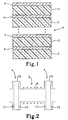
- FIG. 1 illustrates a superlattice structure consisting primarily of an n-doped Group III-Sb material, in which the doping is achieved in accordance with the invention without the use of a Group VI dopant material and its accompanying contamination of the MBE apparatus.
- the structure consists of a series of Group III-Sb base layers 2 that alternate with doping layers 4 formed from a Group III-V compound that has been doped with a suitable n-type dopant, such as silicon or tin.
- the layers are preferably grown with a conventional MBE system, with the growth period for the doping layers 4 considerably shorter than for the base layers 2 so that the doping layers are substantially thinner than the base layers.
- the doping layers 4 are kept thin enough so that, even though their lattices are not closely matched with the lattice structure of the base layers 2, they are established as strained layers that assume the lattice dimensions of the base layers 2 at the junction between the two materials. As described below, mobile electrons from the doping layers 4 drift into the original undoped base layers 2, producing a doping throughout the entire superlattice structure.
- the superlattice characteristics are predominantly III-Sb, since that is the majority material.
- the base layers 2 can consist of any Group III-Sb compound, with Al x Ga 1-x Sb being the preferred formulation for present applications, where x can vary from 0 to 1.0.
- Other compounds such as InGaSb and InAlSb can also be used for the base layers, with varying proportions of In/Ga and In/Al.
- the doping layers 4 have the desired property of accepting a silicon or tin impurity as an n-type dopant, in contrast to the p-type doping action of these impurities in the Sb-compound base layers 2.
- the doping layers 4 are preferably of the form Al y Ga1 ⁇ y As, where y can vary from 0 to 1.0.
- the thicknesses of the doping layers 4 is restricted so they do not exceed the critical thickness above which dislocations are formed at the junctions between the base and doping layers.
- the critical thickness varies with differential materials, but is generally on the order of 2-5 monolayers, with each monolayer typically about 3 Angstroms thick.
- the critical thickness for GaAs on GaSb is about 2-3 monolayers, as compared with a critical thickness of about 5 monolayers for InP on GaSb.
- MBE with InP requires a gas source rather than the solid source used for GaAs, and thus requires more complicated and expensive MBE equipment to implement.
- Group III-V doping layers It may be possible to use virtually any Group III-V combination for the doping layers. However, it is presently uncertain whether compounds with two Group V components, such as GaAsSb or GaPSb, would be doped n-type or p-type by silicon (Sb, As and p are in Group V, while Ga, Al and In are in Group III). Binary or ternary Group III-V doping layers with only a single Group V component are accordingly preferred.
- the overall superlattice 6 is typically several hundred Angstroms thick, with the base layers each about 25-100 Angstroms thick for GaSb; 5-10 base/doping layer periods are typical.
- FIG. 2 is an energy diagram that illustrates the process by which the entire superlattice is doped n-type when the silicon or tin is originally added to only the doping layers 4.
- the base layers 2 are selected to have a lower conduction band energy level, indicated by trace 8, than the conduction band energy level of the doping layers 4, indicated by trace 10.
- the lower conduction band energy base layers have a greater electron affinity, allowing mobile electrons from the doping layers to drift into the base layers and dope them n-type without the addition of any dopant impurities into the base layers.
- the portions 12 of the doping layers immediately adjacent the base layers are preferably left undoped to avoid the risk of the dopant material spilling over into the base layers; the undoped sections of the doping layers are indicated as being bounded by dashed lines in FIG. 2.
- the invention thus makes it possible to produce n-type doping in a Group III-Sb material such as GaSb with a silicon dopant, despite the fact that no non-antimony containing semiconductor materials are presently known that have both a larger conduction band energy than GaSb and a close lattice match with GaSb.
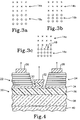
- FIG. 3a illustrates two materials 14a and 16a, whose atoms are indicated respectively by x's and o's, that are closely latticed matched. Their lattice sites match up with each other, and one material can be grown upon the other material by MBE with indefinite thicknesses for both materials.
- the two materials 14b and 16b are not closely lattice matched; material 16b normally has a smaller lattice dimension than material 14b.
- material 16b normally has a smaller lattice dimension than material 14b.
- the lattice structure of material 16b will stretch in the x, y plane parallel to the junction between the two materials, so that the lattices of the two materials align along this junction. This is accompanied by a contraction of the lattice structure for material 16b in the z direction perpendicular to the junction between the two materials.
- FIG. 3c The third situation is illustrated in FIG. 3c.
- material 16c again has a smaller lattice structure than material 14c.
- material 16c is grown to a thickness greater than its critical thickness. This results in the formation of dislocations, consisting of extra columns 18 of material 16c atoms in the z direction, and degrades the electron mobility in the 16c material.
- a strained layer that exhibits such dislocations is referred to as an incoherently strained layer, as opposed to the coherently strained layer of FIG. 3b.
- the thicknesses of the doping layers 4 are preferably restricted as described above so that these layers are coherently strained.
- silicon and tin are the only presently known n-type dopants that work well with MBE.
- the dopant can be combined with the Group III-V material of the doping layers 4 either by opening a silicon or a tin shutter in the MBE apparatus as the doping layers are being grown (except for the undoped portions 12), or by a conventional delta doping technique in which a thin silicon layer is grown in the middle of the doping layer.
- the dopant concentration in the doping layers 6 will typically be within the range of about 1 ⁇ 1016 - 1 ⁇ 1020cm ⁇ 3, which produces a doping concentration in the overall superlattice in the range of about 1 ⁇ 1015 - 1 ⁇ 1019cm ⁇ 3.
- the superlattice itself can form the dopant source for another Group III-Sb compound with which it is fairly closely lattice matched.
- the superlattice base layers 2 are of the form Al x Ga 1-x Sb
- the superlattice can be grown adjacent another layer of Al z Ga 1-z Sb, where z is less than x. Since the reduction in the aluminum content of the second material from x to z also reduces its bandgap energy level, mobile electrons in the superlattice will drift into the adjacent Al z Ga 1-z Sb material and dope it as well.
- FIG. 4 An FET 20 that makes use of the invention is illustrated in FIG. 4.
- the device's source 22 and drain 24 are formed from a doped superlattice as described above, with respective metallized source and drain contacts 26 and 28.
- the central portion of the superlattice between the source and drain is removed, or the two superlattices can be grown separately in the first place with the use of appropriate masks.
- An undoped semiconductor or SiO2 insulating oxide layer 30 capped by a gate contact 32 is then formed over the channel between the two superlattices.
- the superlattice consists of AlGaSb base layers and silicon-doped AlGaAs doping layers, with a total thickness of about 100-300 Angstroms.
- a thin spacer layer 34 is formed between the underside of the superlattice and a channel layer 36.
- the spacer layer which may be AlGaSb, isolates the superlattice dopant from the underlying channel but is thin enough (on the order of 30 Angstroms) so as to not significantly interrupt electron flow between the source and drain and the channel.
- the channel 36 is itself undoped, and may consist of a high mobility material such as In z Ga 1-z As about 120 Angstroms thick, where z is from 0 to 1.0.
- the channel 36 is formed on a buffer layer 38, which is preferably GaSb for AlGaSb base layers in the superlattice, and on the order of 4,000 Angstroms thick.
- the buffer layer in turn is formed on a semi-insulating GaSb substrate 40 that is normally considerably thicker.
- a two-dimensional electron gas (2Deg) is formed along the surface of the channel between the source and drain superlattices in the conventional manner.
- the electron concentration was 2.9 x 1016 cm ⁇ 3, and the electron mobility was 2,704 cm2/v-s.
- the calculated silicon doping densities within the GaAs doping layers were 3.2 ⁇ 1017, 4.9 ⁇ 1017, 3.8 ⁇ 1017, and 4.3 ⁇ 1017cm ⁇ 3 for the first through fourth samples, respectively.
- the observed electron mobility compared favorably with a calculated electron mobility in lightly doped n-type GaSb of about 4,000 cm2/v-s, and further improvements can be expected.
- the invention thus makes it possible to realize heterostructures and superlattices of n-doped, MBE grown Sb compounds without the contamination of the MBE system that results from the conventional use of Group VI dopants. While several illustrative embodiments of the invention have been described, numerous variations and alternate embodiments will occur to those skilled in the art. Such variations and alternate embodiments are contemplated, and can be made without departing from the spirit and scope of the invention as defined in the appended claims.
Landscapes
- Junction Field-Effect Transistors (AREA)
- Physical Deposition Of Substances That Are Components Of Semiconductor Devices (AREA)
Applications Claiming Priority (2)
| Application Number | Priority Date | Filing Date | Title |
|---|---|---|---|
| US86637292A | 1992-04-09 | 1992-04-09 | |
| US866372 | 2001-05-25 |
Publications (2)
| Publication Number | Publication Date |
|---|---|
| EP0565054A2 true EP0565054A2 (de) | 1993-10-13 |
| EP0565054A3 EP0565054A3 (en) | 1994-07-27 |
Family
ID=25347470
Family Applications (1)
| Application Number | Title | Priority Date | Filing Date |
|---|---|---|---|
| EP19930105687 Withdrawn EP0565054A3 (en) | 1992-04-09 | 1993-04-06 | N-type antimony-based strained layer superlattice and fabrication method |
Country Status (3)
| Country | Link |
|---|---|
| US (2) | US5420442A (de) |
| EP (1) | EP0565054A3 (de) |
| JP (1) | JPH0661270A (de) |
Cited By (5)
| Publication number | Priority date | Publication date | Assignee | Title |
|---|---|---|---|---|
| EP0585003A3 (en) * | 1992-08-24 | 1996-01-31 | American Telephone & Telegraph | Group iii-v compound semiconductor device including a group iv element doped region |
| US7224041B1 (en) | 2003-09-30 | 2007-05-29 | The Regents Of The University Of California | Design and fabrication of 6.1-Å family semiconductor devices using semi-insulating A1Sb substrate |
| US20180061973A1 (en) * | 2016-08-25 | 2018-03-01 | Fujitsu Limited | Compound semiconductor device and method of manufacturing the compound semiconductor device |
| EP3314667A4 (de) * | 2015-06-27 | 2019-02-27 | INTEL Corporation | Dotierung einer selbstausgerichteten amphoteren finfet-spitze mit geringer schädigung |
| US10546858B2 (en) | 2015-06-27 | 2020-01-28 | Intel Corporation | Low damage self-aligned amphoteric FINFET tip doping |
Families Citing this family (7)
| Publication number | Priority date | Publication date | Assignee | Title |
|---|---|---|---|---|
| US5668387A (en) * | 1995-10-26 | 1997-09-16 | Trw Inc. | Relaxed channel high electron mobility transistor |
| JP2718406B2 (ja) * | 1995-12-19 | 1998-02-25 | 日本電気株式会社 | 電界効果トランジスタ |
| US5940695A (en) | 1996-10-11 | 1999-08-17 | Trw Inc. | Gallium antimonide complementary HFET |
| US6380552B2 (en) | 1999-05-28 | 2002-04-30 | Hrl Laboratories, Llc | Low turn-on voltage InP Schottky device and method |
| JP3371871B2 (ja) * | 1999-11-16 | 2003-01-27 | 日本電気株式会社 | 半導体装置の製造方法 |
| US7812339B2 (en) * | 2007-04-23 | 2010-10-12 | Mears Technologies, Inc. | Method for making a semiconductor device including shallow trench isolation (STI) regions with maskless superlattice deposition following STI formation and related structures |
| US9214518B1 (en) * | 2014-07-18 | 2015-12-15 | Taiwan Semiconductor Manufacturing Company Limited and National Taiwan University | Using molecular beam epitaxy in a semiconductor structure with a high K/GaSb interface |
Family Cites Families (7)
| Publication number | Priority date | Publication date | Assignee | Title |
|---|---|---|---|---|
| US4517047A (en) * | 1981-01-23 | 1985-05-14 | The United States Of America As Represented By The Secretary Of The Army | MBE growth technique for matching superlattices grown on GaAs substrates |
| DE3480631D1 (de) * | 1983-06-24 | 1990-01-04 | Nec Corp | Halbleiterstruktur mit uebergitter hoher traegerdichte. |
| US4607272A (en) * | 1983-10-06 | 1986-08-19 | The United States Of America As Represented By The United States Department Of Energy | Electro-optical SLS devices for operating at new wavelength ranges |
| US4797716A (en) * | 1984-04-04 | 1989-01-10 | The United States Of America As Represented By The United States Department Of Energy | Field-effect transistor having a superlattice channel and high carrier velocities at high applied fields |
| US4780748A (en) * | 1986-06-06 | 1988-10-25 | American Telephone & Telegraph Company, At&T Bell Laboratories | Field-effect transistor having a delta-doped ohmic contact |
| JP2822547B2 (ja) * | 1990-03-06 | 1998-11-11 | 富士通株式会社 | 高電子移動度トランジスタ |
| JPH03288446A (ja) * | 1990-04-05 | 1991-12-18 | Nec Corp | 2次元電子ガス電界効果トランジスタ |
-
1993
- 1993-04-06 EP EP19930105687 patent/EP0565054A3/en not_active Withdrawn
- 1993-04-09 JP JP5083667A patent/JPH0661270A/ja active Pending
-
1994
- 1994-04-05 US US08/223,373 patent/US5420442A/en not_active Expired - Lifetime
- 1994-04-14 US US08/223,496 patent/US5489549A/en not_active Expired - Lifetime
Cited By (7)
| Publication number | Priority date | Publication date | Assignee | Title |
|---|---|---|---|---|
| EP0585003A3 (en) * | 1992-08-24 | 1996-01-31 | American Telephone & Telegraph | Group iii-v compound semiconductor device including a group iv element doped region |
| US7224041B1 (en) | 2003-09-30 | 2007-05-29 | The Regents Of The University Of California | Design and fabrication of 6.1-Å family semiconductor devices using semi-insulating A1Sb substrate |
| EP3314667A4 (de) * | 2015-06-27 | 2019-02-27 | INTEL Corporation | Dotierung einer selbstausgerichteten amphoteren finfet-spitze mit geringer schädigung |
| US10546858B2 (en) | 2015-06-27 | 2020-01-28 | Intel Corporation | Low damage self-aligned amphoteric FINFET tip doping |
| US20180061973A1 (en) * | 2016-08-25 | 2018-03-01 | Fujitsu Limited | Compound semiconductor device and method of manufacturing the compound semiconductor device |
| EP3291306A1 (de) * | 2016-08-25 | 2018-03-07 | Fujitsu Limited | Verbundhalbleiterbauelement und verfahren zur herstellung eines verbundhalbleiterbauelements |
| US10134889B2 (en) * | 2016-08-25 | 2018-11-20 | Fujitsu Limited | Compound semiconductor device and method of manufacturing the compound semiconductor device |
Also Published As
| Publication number | Publication date |
|---|---|
| JPH0661270A (ja) | 1994-03-04 |
| US5420442A (en) | 1995-05-30 |
| EP0565054A3 (en) | 1994-07-27 |
| US5489549A (en) | 1996-02-06 |
Similar Documents
| Publication | Publication Date | Title |
|---|---|---|
| Daembkes et al. | The n-channel SiGe/Si modulation-doped field-effect transistor | |
| US5663583A (en) | Low-noise and power ALGaPSb/GaInAs HEMTs and pseudomorpohic HEMTs on GaAs substrate | |
| US4163237A (en) | High mobility multilayered heterojunction devices employing modulated doping | |
| EP0312237A2 (de) | Anreicherung der Grenzschichtladung in einer delta-dotierten Heterostruktur | |
| US7951684B2 (en) | Semiconductor device method of manfacturing a quantum well structure and a semiconductor device comprising such a quantum well structure | |
| US6489639B1 (en) | High electron mobility transistor | |
| US9991172B2 (en) | Forming arsenide-based complementary logic on a single substrate | |
| JP3224437B2 (ja) | Iii−v族化合物半導体装置 | |
| US5548140A (en) | High-Speed, low-noise millimeterwave hemt and pseudomorphic hemt | |
| EP0199435B1 (de) | Feldeffekt-Halbleiteranordnung | |
| EP0594442A2 (de) | Schottky-Übergang Anordnung | |
| US5420442A (en) | N-type antimony-based strained layer superlattice | |
| EP0381396A1 (de) | Verbindungshalbleiteranordnungen | |
| US5952672A (en) | Semiconductor device and method for fabricating the same | |
| US6100542A (en) | InP-based HEMT with superlattice carrier supply layer | |
| US20150364547A1 (en) | High-mobility semiconductor heterostructures | |
| US4600932A (en) | Enhanced mobility buried channel transistor structure | |
| Kuech et al. | Field‐effect transistor structure based on strain‐induced polarization charges | |
| EP0602671A2 (de) | Heteroübergangsfeldeffekttransistor mit verbesserter Transistorseigenschaft | |
| Kudo et al. | MBE growth of Si-doped InAlAsSb layers lattice-matched with InAs | |
| JP2557373B2 (ja) | 化合物半導体装置 | |
| JPH01143270A (ja) | 半導体装置 | |
| JPH08213594A (ja) | 電界効果トランジスタ | |
| JP2994863B2 (ja) | ヘテロ接合半導体装置 | |
| JPH06244217A (ja) | ヘテロ接合半導体装置 |
Legal Events
| Date | Code | Title | Description |
|---|---|---|---|
| PUAI | Public reference made under article 153(3) epc to a published international application that has entered the european phase |
Free format text: ORIGINAL CODE: 0009012 |
|
| AK | Designated contracting states |
Kind code of ref document: A2 Designated state(s): DE FR IT |
|
| PUAL | Search report despatched |
Free format text: ORIGINAL CODE: 0009013 |
|
| AK | Designated contracting states |
Kind code of ref document: A3 Designated state(s): DE FR IT |
|
| 18D | Application deemed to be withdrawn |
Effective date: 19950128 |