EP0564364A2 - Method for selectively exposing an uneven substrate surface - Google Patents
Method for selectively exposing an uneven substrate surface Download PDFInfo
- Publication number
- EP0564364A2 EP0564364A2 EP93400856A EP93400856A EP0564364A2 EP 0564364 A2 EP0564364 A2 EP 0564364A2 EP 93400856 A EP93400856 A EP 93400856A EP 93400856 A EP93400856 A EP 93400856A EP 0564364 A2 EP0564364 A2 EP 0564364A2
- Authority
- EP
- European Patent Office
- Prior art keywords
- portions
- prismatic element
- substrate surface
- substrate
- photosensitive material
- Prior art date
- Legal status (The legal status is an assumption and is not a legal conclusion. Google has not performed a legal analysis and makes no representation as to the accuracy of the status listed.)
- Withdrawn
Links
- 239000000758 substrate Substances 0.000 title claims abstract description 85
- 238000000034 method Methods 0.000 title claims abstract description 32
- 239000011248 coating agent Substances 0.000 claims abstract description 28
- 238000000576 coating method Methods 0.000 claims abstract description 28
- 239000000463 material Substances 0.000 claims description 49
- 229920002120 photoresistant polymer Polymers 0.000 abstract description 14
- 230000003287 optical effect Effects 0.000 description 4
- 238000000926 separation method Methods 0.000 description 4
- 239000012799 electrically-conductive coating Substances 0.000 description 3
- 239000012530 fluid Substances 0.000 description 3
- 230000002238 attenuated effect Effects 0.000 description 2
- 230000007423 decrease Effects 0.000 description 2
- 239000011521 glass Substances 0.000 description 2
- 239000004973 liquid crystal related substance Substances 0.000 description 2
- 239000007787 solid Substances 0.000 description 2
- VYPSYNLAJGMNEJ-UHFFFAOYSA-N Silicium dioxide Chemical compound O=[Si]=O VYPSYNLAJGMNEJ-UHFFFAOYSA-N 0.000 description 1
- 238000010521 absorption reaction Methods 0.000 description 1
- 239000003795 chemical substances by application Substances 0.000 description 1
- 230000003247 decreasing effect Effects 0.000 description 1
- 239000008367 deionised water Substances 0.000 description 1
- 229910021641 deionized water Inorganic materials 0.000 description 1
- 230000000694 effects Effects 0.000 description 1
- 239000005350 fused silica glass Substances 0.000 description 1
- AMGQUBHHOARCQH-UHFFFAOYSA-N indium;oxotin Chemical compound [In].[Sn]=O AMGQUBHHOARCQH-UHFFFAOYSA-N 0.000 description 1
- 239000007788 liquid Substances 0.000 description 1
- 230000000873 masking effect Effects 0.000 description 1
- QSHDDOUJBYECFT-UHFFFAOYSA-N mercury Chemical compound [Hg] QSHDDOUJBYECFT-UHFFFAOYSA-N 0.000 description 1
- 238000002360 preparation method Methods 0.000 description 1
- 230000005855 radiation Effects 0.000 description 1
- 239000012858 resilient material Substances 0.000 description 1
- 239000002904 solvent Substances 0.000 description 1
- XLYOFNOQVPJJNP-UHFFFAOYSA-N water Chemical compound O XLYOFNOQVPJJNP-UHFFFAOYSA-N 0.000 description 1
Images

Classifications
-
- G—PHYSICS
- G03—PHOTOGRAPHY; CINEMATOGRAPHY; ANALOGOUS TECHNIQUES USING WAVES OTHER THAN OPTICAL WAVES; ELECTROGRAPHY; HOLOGRAPHY
- G03F—PHOTOMECHANICAL PRODUCTION OF TEXTURED OR PATTERNED SURFACES, e.g. FOR PRINTING, FOR PROCESSING OF SEMICONDUCTOR DEVICES; MATERIALS THEREFOR; ORIGINALS THEREFOR; APPARATUS SPECIALLY ADAPTED THEREFOR
- G03F7/00—Photomechanical, e.g. photolithographic, production of textured or patterned surfaces, e.g. printing surfaces; Materials therefor, e.g. comprising photoresists; Apparatus specially adapted therefor
- G03F7/20—Exposure; Apparatus therefor
- G03F7/2002—Exposure; Apparatus therefor with visible light or UV light, through an original having an opaque pattern on a transparent support, e.g. film printing, projection printing; by reflection of visible or UV light from an original such as a printed image
-
- Y—GENERAL TAGGING OF NEW TECHNOLOGICAL DEVELOPMENTS; GENERAL TAGGING OF CROSS-SECTIONAL TECHNOLOGIES SPANNING OVER SEVERAL SECTIONS OF THE IPC; TECHNICAL SUBJECTS COVERED BY FORMER USPC CROSS-REFERENCE ART COLLECTIONS [XRACs] AND DIGESTS
- Y10—TECHNICAL SUBJECTS COVERED BY FORMER USPC
- Y10S—TECHNICAL SUBJECTS COVERED BY FORMER USPC CROSS-REFERENCE ART COLLECTIONS [XRACs] AND DIGESTS
- Y10S438/00—Semiconductor device manufacturing: process
- Y10S438/942—Masking
- Y10S438/948—Radiation resist
- Y10S438/949—Energy beam treating radiation resist on semiconductor
Definitions
- the present invention relates to a method and apparatus for exposing to light selected portions of an uneven substrate surface without the use of a mask.
- the method may be used to remove a coating from either the upper or lower portions of the uneven substrate surface.
- patterns of light may be formed by directing light rays through a mask toward a flat surface.
- This masking method may also be used to selectively remove a photosensitive material from a flat surface: the photosensitive material is applied to the flat surface; the mask is placed on top of the photosensitive material; light is directed through the mask to the photosensitive material; and then either the exposed or unexposed photosensitive material is removed, depending upon whether a "positive” or "negative” type of photosensitive material is used.
- a mask may also be used to expose to light selected portions of a surface having upper and lower portions.
- a mask may also be used to expose to light selected portions of a surface having upper and lower portions.
- the disadvantage of this approach is that as the distances between the raised portions of the substrate surface become increasingly small (eg. on the order of 100 ⁇ m), the problem of aligning the mask and substrate surface becomes increasingly large.
- U.S. Patent No. 4,670,095 to Negishi discloses a maskless method for selectively exposing the sides of a sawtoothed-ridged surface (such as a fresnel plate).
- a photosensitive agent may be selectively removed from the sides of the sawtoothed ridges by projecting light rays toward the photosensitive-covered surface at an oblique angle so that the sides of the ridges which face the light are exposed, while the opposite sides of the ridges are not exposed. While this method may be useful for removing photosensitive material from the sides of sawtoothed-shaped ridges, the method is less effective at removing photosensitive material from the tops of rectangular-shaped ridges (ie.
- ridges having substantially vertical walls and a horizontal top because the oblique light would not be normal to the horizontal surface of the tops of the rectangular ridges, thus decreasing the efficiency of the exposure, as well as exposing the sides of the ridges which face the light source, which may be undesirable.
- this "shadow" method becomes increasingly less effective as the distance between the ridges increases and the height of the ridges decreases, making it difficult to expose the tops of the ridges without also exposing the lower surface of the substrate between the ridges. It would be desirable to have an effective method for exposing the raised portions of a substrate surface without exposing the lower portions of the surface, even where the height of the raised portions is small compared with the distance between them.
- the present invention is a method for selectively removing a coating (such as an electrically conductive coating) from either the upper or lower portions of an uneven surface by: applying a layer of photosensitive material over the coated substrate; placing a prismatic element on the photosensitive-covered, substrate surface; projecting light rays through the prismatic element toward the substrate surface so that the portions of the photosensitive material proximate the prismatic element are exposed to the light rays, while the portions of the photosensitive material not proximate the prismatic element are left unexposed; removing those portions of the photosensitive material which are soluble in developer; and removing those portions of the coating which are no longer covered by the photosensitive material.
- the photosensitive material which remains may also be removed.
- One embodiment of the present invention includes a method for selectively exposing portions of a substrate surface having upper and lower portions, including: (1) placing a prismatic element adjacent a substrate surface having upper and lower portions; and (2) projecting light rays from a light source through the prismatic element toward the substrate surface so that the portions of the substrate surface proximate the prismatic element are exposed to said light rays, while the portions of the substrate not proximate the prismatic element are left unexposed.
- the light source may be any conventional source emitting radiation to which the photosensitive material is sensitive.
- the light source may be a laser which can be used to melt or ablate the portions of the substrate surface which are exposed to the light rays.
- Another embodiment of the present invention includes an apparatus for selectively exposing portions of a substrate surface in a step and repeat mode. Yet another embodiment of the present invention includes an apparatus for selectively exposing portions of a flexible substrate surface in a continuous mode.
- the present invention finds particular utility in the preparation of liquid crystal substrates containing integral spacing elements, such as a series of parallel ridges, where it is desired to have a previously applied electrically conductive coating selectively removed from the top surface of the spacing elements.
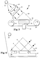
- a substrate 12 having a series of raised, parallel, rectangular ridges 16 covered with a coating 14 is shown in FIGURE 1.
- substrate 12 can be a half-cell for a liquid crystal display device
- coating 14 can be an electrically conductive coating, such as indium tin oxide (ITO) wherein coating 14 is applied to the surface of the substrate to form electrodes for switching the device.
- ITO indium tin oxide
- the half-cell is then mated with another similar half-cell to form a display device having an X-Y array of electrodes.
- the method of the present invention is particularly wuited to this purpose.
- the first step of the present invention involves applying a layer of photosensitive material 18 over coating 14, as shown in FIGURE 4.
- Prismatic element 20 is then placed in contact with the coated ridges 16 of substrate 12.
- Prismatic element 20 preferably is a right-angle (or 45-45-90) prism in which the light enters generally normal to a face opposite to a 45° angle, is totally reflected at the hypotenuse face, and leaves by the third face, thus having been totally reflected through 90°.
- a light source 22 directs collimated light perpendicular to the surface of prismatic element 20, as shown in FIGURE 4.
- a ray of light traveling in a generally downward direction in prismatic element 20 will be totally reflected at the lower surface thereof provided that the sine of the angle between ray A and a normal to the lower surface of prismatic element 20 is greater than the ratio of the refractive index, n1, of the material below prismatic element 20 to the refractive index, n2, of prismatic element 20.
- light rays, such as A will be totally reflected wherever prismatic element 20 is not in contact with photosensitive material 18.
- ray A will be reflected at the prism/substrate interface, and the underlying photosensitive material 18 will not be exposed.
- the intensity of transmitted ray B'' may be increased by selecting a photosensitive material 18 having an index of refraction which is close to the index of refraction of prismatic element 20. The intensity of transmitted ray B'' should be high enough to cause the desired change in photosensitive material 18.
- the intensity of transmitted ray B'' will decrease (but will not become zero) if photosensitive layer 18 is separated from prismatic element 20 by a distance which is small compared with the wavelength of light being used. This is so because light is not totally internally reflected within a prism when there is an object within a distance from the prism that is smaller than the wavelength of light being used (where the object has an index of refraction greater than air, ie. greater than 1.0).
- the separation d between the prismatic element 20 and photosensitive material 18 is greater than about 0.4 ⁇ m (for light of wavelength 400 nm)
- the photosensitive material 18 will not be exposed.
- separations d of less than 0.4 ⁇ m some of the photosensitive material will be exposed, depending upon the magnitude of separation d, the length of the exposure time, and the intensity of light source 22.
- prismatic element 20 should be in contact with photosensitive layer 18 at all portions that are desired to be exposed.
- the separation d between the two should not exceed 0.2 ⁇ m.
- proximate will be used hereinafter to denote a distance of 0.2 ⁇ m or less.
- Substrate 12 may be held against prismatic element 20 by applying force to pressure pad 26, as shown in FIGURES 4 and 5.
- light ray B'' may continue through substrate 12 until it reaches the lower side of substrate 12. If the lower side of substrate 12 is adjacent a layer of air, ray B'' could be reflected back toward photosensitive material 18, where it could expose areas of the photosensitive material which were not intended to be exposed. The amount of light reflected depends on the fresnel coefficient of reflection for that interface. For this reason, a light absorbing layer 24 is preferably placed below substrate 12.
- Photosensitive material 18 on the tops of ridges 16 is exposed to light in the manner described above.
- Photosensitive material 18 is preferably a material commonly referred to as photoresist.
- photoresist is divided into two types: positive and negative.
- positive photoresist the portion of the photoresist on the tops of ridges 16 which was exposed to the light rays can be developed off, such as by dissolving with a solvent, revealing coating 14 underneath. Those portions between ridges 16 which are not exposed to light rays remain.
- the remaining photoresist is then rinsed with deionized water, dried, and oven baked to toughen it. Light rays having a wavelength in the range of 350-450 nm are preferred for most types of photoresist.
- the coating 14 on the tops and upper sides of ridges 16 revealed by the selective removal of photoresist layer 18 may now be etched off because those portions of coating 14 are no longer protected by the photoresist.
- the remaining photoresist may then be removed by methods familiar to those skilled in the art.
- the uniform coating 14 shown in FIGURE 1 is removed from the tops of ridges 16, as shown in FIGURE 2.
- portions of coating 14 located on the bottom of substrate 12 and on the lower sides of ridges 16 may be removed in a manner analogous to that described above by using negative photoresist or positive photoresist in the negative mode.
- those portions of coating 14 lying beneath the portions of the photoresist which are not exposed because they are not proximate prismatic element 20 may be removed.
- the result is that the uniform coating 14 shown in FIGURE 1 is removed from the bottom of substrate 12 (ie. between ridges 16), as shown in FIGURE 3.
- ridges 16 are oriented parallel to the apex of prismatic element 20. With this geometry, the photosensitive material 18 on the upper right side of the ridges 16 will be exposed to more light than the photosensitive material 18 on the left side. If, however, the right face of prismatic element 20 were also illuminated with collimated light from a second light source (not shown), then the photosensitive material 18 on the upper portion of both sides of ridges 16 would be exposed.
- the right face of prismatic element 20 may be aluminized to accomplish a similar result. If this were done, light rays A' and B' would be reflected back along their respective paths.
- An analysis of the light ray paths through photosensitive material 18 on the right side of ridges 16 shows that, for a typical case, light incident on the photoresist-air interface would be totally internally reflected. Some of the incident light rays would, however, be attenuated by optical absorption in coating 14.
- ridges 16 be perpendicular to the apex of prismatic element 20.
- light which is transmitted into photosensitive material 18 near the side walls of ridges 16 can expose the photosensitive material 18 on the side walls without being attenuated by passing through coating 14. This is advantageous where it is desired to remove coating 14 from the sides of ridges 16.
- the method of the present invention may also be used to etch the tops of ridges 16 on substrate 12, as shown in FIGURE 6.
- Light rays passing through prismatic element 20 will illuminate those portions of substrate 12 which are proximate to the prismatic element.
- light source 22 can be a laser which directs high intensity, collimated light rays through prismatic element 20 toward substrate 12 to the tops of ridges 16 (so long as the tops of the ridges are proximate the prismatic element).
- the laser can be used to melt or ablate the tops of ridges 16.
- This apparatus can also be used to melt or ablate a coating (not shown) on the tops of ridges 16 of substrate 12.
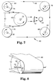
- the method of the present invention may be practiced on large area samples in a step and repeat mode with the use of apparatus 50, shown in FIGURE 5.
- Prismatic element 20 is suspended over adjustable table 30.
- Pressure pad 26 is placed on top of table 30 and is supported by rigid backing plate 32.
- Pressure pad 26 is made of a resilient material to ensure good physical contact between prismatic element 20 and the tops of ridges 16 on substrate 12.
- Table 30 is made adjustable through the use of pneumatic cylinder 34.
- Rollers 36 and 38 power transport belt 40, which is interposed between pressure pad 26 and prismatic element 20.
- condensing lens 42 which is preferably a large diameter plano-convex condenser lens made of PyrexTM or similar material which transmits light in the wavelength rage of 350-450 nm.
- Light source 22 is a high intensity, small area light source such as a high pressure mercury vapor lamp.
- An electrically operated shutter 44 may be used to control exposure duration.
- the sample to be treated (not shown) is placed on transport belt 38, which moves the sample into place between prismatic element 20 and pressure pad 26. Pneumatic cylinder 34 then forces pressure pad 26 up against belt 40, thus forcing the sample against prismatic element 20. (The force used should not be so great that the lower portions of the sample surface are forced against prismatic element 20.)
- the sample is illuminated by the prism method discussed earlier, and then cylinder 34 retracts, lowering the sample away from prismatic element 20. The sample then moves along on belt 40 to its next destination.
- Prismatic element 20 may be a solid glass prism made of a material such as BK7 (Schottglass). Alternatively, a hollow prism of fused silica plates cemented together on the edges and filled with an index matching fluid can be used. A suitable index matching fluid is made by R.P. Cargille Laboratories, Inc. (Specialty Optical Fluid No. 50350 or No. 06350). The principal advantage of a liquid-filled prism over a solid prism is cost. Alternatively, prismatic element 20 may be a series of tiny, parallel, adjacent prisms, such as ScotchTM Optical Lighting Film.
- the method of the present invention may be practiced on large area samples in a continuous mode with the use of apparatus 60, shown in FIGURE 7.
- Belt 82 is wound about rolls 62, 64, 66, 68, and 70, which are mounted for rotation about axes 72, 74, 76, 78, and 80, respectively.
- Belt 82 is a transparent film having a series of tiny, parallel adjacent prismatic elements, such as ScotchTM Optical Lighting Film.
- the surface of belt 82 having the prismatic elements faces toward light source 22 as the belt moves around roll 62.
- Substrate 16 is flexible and is wound about roll 62 and other rolls (not shown). The surface of substrate 16 to be exposed to light faces away from roll 62. Light source 22 and condensing lens 42 are located within the continuous loop formed by belt 82.
- one end of substrate 16 is drawn away from roll 62 by a motor (not shown). This forces a counter-clockwise rotation of roll 62 on its axis 72, which in turn draws additional portions of substrate 16 around and past the roll.
- belt 82 does not directly contact roll 62 but rather contacts the surface of substrate 16 to be exposed.
- the orientation of roll 62 with respect to rolls 64 and 70 forces belt 82 to press tightly against substrate 16 on the side of roll 62 which faces light source 22. This pressure prevents belt 82 from moving with respect to substrate 16 at the point of contact.
- the counter-clockwise rotation of roll 62 causes a clockwise rotation of rolls 64, 66, 68, and 70, which creates a generally clockwise path of travel for belt 82, as shown in FIGURE 7.
- Light rays from light source 22 are collimated by condensing lens 42 toward the tiny prisms on belt 18.
- Light rays from light source 22 expose the portions of the surface of substrate 16 which are proximate belt 18.
- the rate of rotation of the rolls, the tension of belt 82, and the intensity of light source 22 may be adjusted to create the desired exposure of substrate 16.
Landscapes
- Physics & Mathematics (AREA)
- General Physics & Mathematics (AREA)
- Exposure And Positioning Against Photoresist Photosensitive Materials (AREA)
- ing And Chemical Polishing (AREA)
Applications Claiming Priority (2)
| Application Number | Priority Date | Filing Date | Title |
|---|---|---|---|
| US07/863,402 US5292625A (en) | 1992-04-03 | 1992-04-03 | Method for selectively exposing an uneven substrate surface |
| US863402 | 1992-04-03 |
Publications (2)
| Publication Number | Publication Date |
|---|---|
| EP0564364A2 true EP0564364A2 (en) | 1993-10-06 |
| EP0564364A3 EP0564364A3 (enExample) | 1995-01-18 |
Family
ID=25341038
Family Applications (1)
| Application Number | Title | Priority Date | Filing Date |
|---|---|---|---|
| EP93400856A Withdrawn EP0564364A2 (en) | 1992-04-03 | 1993-04-02 | Method for selectively exposing an uneven substrate surface |
Country Status (4)
| Country | Link |
|---|---|
| US (1) | US5292625A (enExample) |
| EP (1) | EP0564364A2 (enExample) |
| JP (1) | JPH0649673A (enExample) |
| KR (1) | KR930022146A (enExample) |
Cited By (1)
| Publication number | Priority date | Publication date | Assignee | Title |
|---|---|---|---|---|
| US6077560A (en) * | 1997-12-29 | 2000-06-20 | 3M Innovative Properties Company | Method for continuous and maskless patterning of structured substrates |
Families Citing this family (7)
| Publication number | Priority date | Publication date | Assignee | Title |
|---|---|---|---|---|
| US5365356A (en) * | 1992-08-11 | 1994-11-15 | Minnesota Mining And Manufacturing Company | Method of fabricating an encapsulated liquid crystal display |
| US5629784A (en) * | 1994-04-12 | 1997-05-13 | Ois Optical Imaging Systems, Inc. | Liquid crystal display with holographic diffuser and prism sheet on viewer side |
| US5963284A (en) * | 1998-04-01 | 1999-10-05 | Ois Optical Imaging Systems, Inc. | LCD with diffuser having diffusing particles therein located between polarizers |
| EP1001311A1 (en) * | 1998-11-16 | 2000-05-17 | International Business Machines Corporation | Patterning device |
| US7354519B1 (en) | 2003-02-03 | 2008-04-08 | Hutchinson Technology Incorporated | Method and apparatus for fabricating a stent |
| US8097400B2 (en) * | 2005-02-22 | 2012-01-17 | Hewlett-Packard Development Company, L.P. | Method for forming an electronic device |
| US8803028B1 (en) | 2005-04-13 | 2014-08-12 | Genlyte Thomas Group, Llc | Apparatus for etching multiple surfaces of luminaire reflector |
Family Cites Families (8)
| Publication number | Priority date | Publication date | Assignee | Title |
|---|---|---|---|---|
| CA827832A (en) * | 1969-11-18 | E. Clark Harold | Image formation and projection | |
| DE1252061B (enExample) * | 1962-07-02 | |||
| NL7808899A (nl) * | 1978-08-30 | 1980-03-04 | Philips Nv | Weergeefinrichting met vloeibaar kristal. |
| US4218302A (en) * | 1979-08-02 | 1980-08-19 | U.S. Philips Corporation | Electrophoretic display devices |
| JPS60230601A (ja) * | 1984-05-01 | 1985-11-16 | Masayasu Negishi | 膜処理方法 |
| JPS61156003A (ja) * | 1984-12-27 | 1986-07-15 | Sharp Corp | 回折格子の製造方法 |
| CA1270934C (en) * | 1985-03-20 | 1990-06-26 | SPATIAL PHASE MODULATED MASKS AND METHODS FOR MAKING THESE MASKS AND PHASE DIFFRACTION GRATINGS | |
| GB8629223D0 (en) * | 1986-12-06 | 1987-01-14 | Emi Plc Thorn | Replication of carriers |
-
1992
- 1992-04-03 US US07/863,402 patent/US5292625A/en not_active Expired - Lifetime
-
1993
- 1993-04-02 EP EP93400856A patent/EP0564364A2/en not_active Withdrawn
- 1993-04-02 JP JP5076778A patent/JPH0649673A/ja active Pending
- 1993-04-02 KR KR1019930005570A patent/KR930022146A/ko not_active Withdrawn
Cited By (1)
| Publication number | Priority date | Publication date | Assignee | Title |
|---|---|---|---|---|
| US6077560A (en) * | 1997-12-29 | 2000-06-20 | 3M Innovative Properties Company | Method for continuous and maskless patterning of structured substrates |
Also Published As
| Publication number | Publication date |
|---|---|
| EP0564364A3 (enExample) | 1995-01-18 |
| KR930022146A (ko) | 1993-11-23 |
| JPH0649673A (ja) | 1994-02-22 |
| US5292625A (en) | 1994-03-08 |
Similar Documents
| Publication | Publication Date | Title |
|---|---|---|
| JP2718421B2 (ja) | 画像投射装置 | |
| US5292625A (en) | Method for selectively exposing an uneven substrate surface | |
| EP0913720A3 (en) | Irradiation device for an alignment layer of a liquid crystal cell element | |
| US12174547B2 (en) | Non-telecentric light guide elements | |
| KR100990074B1 (ko) | 경사 노광 리소그래피 시스템 | |
| US6262795B1 (en) | Apparatus and method for the improvement of illumination uniformity in photolithographic systems | |
| JP3384346B2 (ja) | 液晶表示素子の光配向用偏光光照射装置 | |
| NL1031824C2 (nl) | Een nieuwe inrichting en werkwijze voor immersie lithografie. | |
| US4904087A (en) | Method for aligning photomasks | |
| US5405733A (en) | Multiple beam laser exposure system for liquid crystal shutters | |
| TW200813660A (en) | Apparatus and method for alignment using multiple wavelengths of light | |
| JP3095855B2 (ja) | 外観検査用投光装置 | |
| JPH1082622A (ja) | 基板の検査装置 | |
| KR101040028B1 (ko) | 평판형 표시 장치의 도광판 제조 시스템 및 제조 방법 | |
| CN1320407C (zh) | 一种修复掩膜上的铬污染点的方法及其所采用的定位版 | |
| JPH11274060A5 (enExample) | ||
| CN212460305U (zh) | 一种半导体的制作治具及制作设备 | |
| JP3253942B2 (ja) | 外観検査用投光装置 | |
| KR19990031146A (ko) | 액정 표시 장치 및 그 제조 방법 | |
| JPS5854495B2 (ja) | 位置合わせ方法および光学装置 | |
| JP2622841B2 (ja) | 露光装置 | |
| JPH04109760U (ja) | 露光装置 | |
| KR20000064281A (ko) | 조망스크린및그제조방법 | |
| JPH0293536A (ja) | 半導体装置製造用液晶マスク | |
| JP4883467B2 (ja) | 光量計測装置、露光装置、およびデバイスの製造方法 |
Legal Events
| Date | Code | Title | Description |
|---|---|---|---|
| PUAI | Public reference made under article 153(3) epc to a published international application that has entered the european phase |
Free format text: ORIGINAL CODE: 0009012 |
|
| AK | Designated contracting states |
Kind code of ref document: A2 Designated state(s): DE FR NL |
|
| PUAL | Search report despatched |
Free format text: ORIGINAL CODE: 0009013 |
|
| AK | Designated contracting states |
Kind code of ref document: A3 Designated state(s): DE FR NL |
|
| STAA | Information on the status of an ep patent application or granted ep patent |
Free format text: STATUS: THE APPLICATION IS DEEMED TO BE WITHDRAWN |
|
| 18D | Application deemed to be withdrawn |
Effective date: 19950719 |