EP0563511B1 - Decoder für Informationsströme in einem synchronen digitalen Nachrichten-Transportsystem - Google Patents
Decoder für Informationsströme in einem synchronen digitalen Nachrichten-Transportsystem Download PDFInfo
- Publication number
- EP0563511B1 EP0563511B1 EP19930100460 EP93100460A EP0563511B1 EP 0563511 B1 EP0563511 B1 EP 0563511B1 EP 19930100460 EP19930100460 EP 19930100460 EP 93100460 A EP93100460 A EP 93100460A EP 0563511 B1 EP0563511 B1 EP 0563511B1
- Authority
- EP
- European Patent Office
- Prior art keywords
- byte
- module
- bits
- bytes
- counter
- Prior art date
- Legal status (The legal status is an assumption and is not a legal conclusion. Google has not performed a legal analysis and makes no representation as to the accuracy of the status listed.)
- Expired - Lifetime
Links
- 230000001360 synchronised effect Effects 0.000 title claims description 15
- 230000008878 coupling Effects 0.000 claims description 10
- 238000010168 coupling process Methods 0.000 claims description 10
- 238000005859 coupling reaction Methods 0.000 claims description 10
- 230000015654 memory Effects 0.000 claims description 8
- 230000001747 exhibiting effect Effects 0.000 claims 1
- 238000012163 sequencing technique Methods 0.000 claims 1
- 230000006870 function Effects 0.000 description 6
- 230000007246 mechanism Effects 0.000 description 6
- 230000005540 biological transmission Effects 0.000 description 4
- 238000010586 diagram Methods 0.000 description 2
- 238000011156 evaluation Methods 0.000 description 2
- RGNPBRKPHBKNKX-UHFFFAOYSA-N hexaflumuron Chemical compound C1=C(Cl)C(OC(F)(F)C(F)F)=C(Cl)C=C1NC(=O)NC(=O)C1=C(F)C=CC=C1F RGNPBRKPHBKNKX-UHFFFAOYSA-N 0.000 description 2
- 238000005259 measurement Methods 0.000 description 2
- 230000007704 transition Effects 0.000 description 2
- 241001136792 Alle Species 0.000 description 1
- 230000006978 adaptation Effects 0.000 description 1
- 230000008859 change Effects 0.000 description 1
- 238000004891 communication Methods 0.000 description 1
- 238000005516 engineering process Methods 0.000 description 1
- 238000007667 floating Methods 0.000 description 1
- 230000010354 integration Effects 0.000 description 1
- 238000000034 method Methods 0.000 description 1
- 238000012544 monitoring process Methods 0.000 description 1
- 230000003287 optical effect Effects 0.000 description 1
- 230000008569 process Effects 0.000 description 1
- 238000011160 research Methods 0.000 description 1
- 230000002123 temporal effect Effects 0.000 description 1
Images


Classifications
-
- H—ELECTRICITY
- H04—ELECTRIC COMMUNICATION TECHNIQUE
- H04Q—SELECTING
- H04Q11/00—Selecting arrangements for multiplex systems
- H04Q11/04—Selecting arrangements for multiplex systems for time-division multiplexing
- H04Q11/0428—Integrated services digital network, i.e. systems for transmission of different types of digitised signals, e.g. speech, data, telecentral, television signals
- H04Q11/0478—Provisions for broadband connections
-
- H—ELECTRICITY
- H04—ELECTRIC COMMUNICATION TECHNIQUE
- H04J—MULTIPLEX COMMUNICATION
- H04J3/00—Time-division multiplex systems
- H04J3/16—Time-division multiplex systems in which the time allocation to individual channels within a transmission cycle is variable, e.g. to accommodate varying complexity of signals, to vary number of channels transmitted
- H04J3/1605—Fixed allocated frame structures
- H04J3/1611—Synchronous digital hierarchy [SDH] or SONET
-
- H—ELECTRICITY
- H04—ELECTRIC COMMUNICATION TECHNIQUE
- H04J—MULTIPLEX COMMUNICATION
- H04J2203/00—Aspects of optical multiplex systems other than those covered by H04J14/05 and H04J14/07
- H04J2203/0001—Provisions for broadband connections in integrated services digital network using frames of the Optical Transport Network [OTN] or using synchronous transfer mode [STM], e.g. SONET, SDH
- H04J2203/0089—Multiplexing, e.g. coding, scrambling, SONET
Definitions
- the invention relates to a decoder for information streams in a synchronous digital message transport system according to the preamble of claim 1.
- SDH Synchronous Digital Hierarchy
- SONET Synchronous Optical Transmission Network
- the following figure shows the block format of a synchronous transport module (STM-1).
- SOH section Overhead
- the content can also consist of a multiplex of 3 smaller formats. These then transport the messages from one channel (A, B, C), and the pointer consisting of 6 bytes is divided into 3 pointers each 2 bytes long. The 6-byte variation range is also broken down into 3 parts, each 2 bytes long.
- the block formats of channels A, B, C are 87 lines long and can be used independently with one pointer each in the STM-1 be moved.
- Containers are together with additional system-internal information transmitted for the transmission path. This is called Path Overhead (POH). That from the container and the format composed of POH is called Virtual Container (VCx) designated.
- POH Path Overhead
- VCx Virtual Container
- the 261-line block format contains a so-called virtual container VC-4, in which there is a path overhead (POH) and the bit stream of a channel for the speed 139 264 kbit / s. 0001 POH 0262 POH 0523 POH 0784 POH 1045 POH 1306 POH 1567 POH 1828 POH 2089 POH 0002 C. 0263 C. 0524 C. 0785 C. 1046 C. 1307 C. 1568 c 1829 c 2090 C. 0003 C. 0264 C. 0525 C. 0786 C. 1047 C. 1308 C. 1569 c 1830 c 2091 C. 0261 C. 0522 C. 0783 C. 1044 C. 1305 C. 1566 c 1827 c 2088 C. 2349 C.
- POH path overhead
- the 87-line block format contains a virtual container VC-3, in which there is a path overhead (POH) and the bit stream of a channel for the speed 44 736 kbit / s or 34 368 kbit / s.
- POH path overhead
- the 85-line block format holds the virtual container VC-3, which contains a path overhead (POH) and the bit stream of a channel for the speed 44 736 kbit / s or 34 368 kbit / s.
- POH path overhead
- each of the 3 VC-3 in the VC-4 there can also be 7 VC-2. These are assigned to channels A, B, C, D, E, F, G.
- the format of the VC-2 and the VC-12 and VC-11 mentioned below are defined within 4 consecutive STM-1 frames F1 ... F4, namely a quad frame (QF).
- a multiframe indicator H4 in the POH (POS 1306) numbers the frames within the QF.
- Each VC-2 is preceded by a pointer byte in each frame, and the VC-3 pointer is replaced by a zero pointer indicator (NPI). So if z. B.
- the VC-3 channel C there are seven VC-2 channels, so are in pos. 0006, 0267, 0528 NPI bytes, and in the first positions of type CA, CB, CC, CD, CE, CF, CG the pointer bytes of VC-2 channels A, B, C, D, E, F, G.
- Each of the three 87-line VC-3s in the STM-1 can also accommodate 7 VC-2s. This then results in the following division of the VC-3 concerned:
- one VC-2 can be replaced by three VC-12 or 4 VC-11.
- the beginning of each of these formats is defined with a 2 byte pointer (PTR):
- the content of these formats is therefore 1 byte shorter in each subframe and 4 bytes shorter in the quadframe.
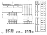
- Figure 3 shows the possible VC combinations in an STM-1.
- the Block formats are with clear, based on the block size Designations (BF %) provided. Variants of the same block size are included Distinguish lowercase letters (a, b ).
- EP-A-0 440 128 discloses a decoder for information streams in one Synchronous digital message transport system with the features of The preamble of claim 1.
- This known arrangement serves the purpose of Message transmission in the SDH system to form required channels in the Messages are entered and from which these are as true to the original as possible be returned again.
- This arrangement is for measuring and Surveillance tasks are not suitable as one suitable arrangement for the measurement technology also with regard to the adaptation to the existing hierarchical configuration in the case of measurement flexible, that is, light and must be clearly manageable.
- the invention is based, preferably to the task Measuring and monitoring purposes the contents of the overheads and decode individual user channels from the STM.
- a circuit structure has to be defined by loading appropriate programs of the variety of STM content can be adjusted and thus regarding the task the SDH architecture and similar architectures controlled. It is advantageous to recognize that it sufficient to decode a VC of a low hierarchical level only the chain of pointers too follow.
- a pointer is used for the implemented format to decode the overhead and to find the pointer for the format implemented there. The last pointer is used to find the format start for the desired one Channel. With this strategy, everyone is overhead Bytes and the content of the relevant channel from the STM byte sequence decodable.
- the counters can in the usual way with individual Binary memories (flip-flops) can be built up one below the other are combined with combinatorial gate logic.
- the counter structure must then be adjustable on a case-by-case basis that the necessary setting and counting functions each be carried out.
- the counters are each programmable Step switch realized that from a RAM (Random Access Memory) and an OWM (One Word Memory).
- the RAM is loaded and located with a certain content to carry out the desired function in the Reading mode.
- the OWM has an input and an output for a certain Briton and takes over with a control impulse the input word into memory, the stored one Content pending at its exit.
- the N bit wide output word of the OWM is on the address input of the RAM. This gives you a rear derailleur for a maximum of 2 ⁇ N states whose transitions through the RAM content can be defined.
- the value of the word of width N at the OWM output represents the current state of the corresponding value at the OWM input the next state. The transition is carried out with the switching pulse.
- P be the pointer value that specifies how many bytes after the last pointer byte the beginning of the block format to be decoded lies.
- the rear derailleur is designed as a reverse counter and immediately after the pointer value arrives at it set.
- the counter runs in an F byte long format cyclically with X MOD F in the range F-1 ... 0, thus reached P steps after the last pointer byte as the beginning of the block declared state O. Orientation to the Block content is given from the moment of setting.
- the word width for the transmission of the pointer value is limited to 10 bits. Since the range of values for a byte-by-byte definition is not sufficient, the pointer defines groups of three in the larger formats (tribytes). On the other hand, the switch mechanism should count single bytes. This discrepancy was taken into account by an embodiment according to the invention in that the counting position of the switching mechanism is set to four times the pointer value. This is done by coupling the pointer word with a 2-bit shift. For example, the decimal pointer value 782 corresponds to the binary number 11 0000 1110. This has 10 digits. Shifting the coupling by 2 bits causes 2 zeros to be appended.
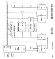
- FIG. 1 shows the function of an arrangement according to the invention on the basis of the function of the control stage for the STM-1 level and in relation to the hierarchical level below it.
- An STM byte former (SBF) which is not further broken down, receives the STM-1 bit stream, monitors it for the sync word, emits a sync pulse after the last byte of the 6 byte long sync word and then converts the bit stream into a byte sequence. Each valid byte is identified by a byte clock.
- the first counter 1 for the 2340 byte positions of the STM-1 consists of a RAM and an OWM. It is set by the synchronous pulse of the SBF. For the sync word can do this like a pointer with a fixed value to be viewed as.
- Counting is the counting sequence for the STM-1 0000 - 3239 - 3238 - 3236 - 3235 - 3234 - 3232 - ... and after the sixth byte must the value 3232 is set.
- the fixed tribyte pointer value is due to the by 2 Make offset coupling equal to the fourth part of the set value, i.e. 808.
- counter 1 defines for each byte position of the STM-1 a certain counting state. This means that it can have one RAM each Assign address for overhead bytes to be stored and a memory pulse release. This RAM then takes the bytes in question directly the STM-1 byte sequence.
- Counter 1 also controls a "Pointer Control” module. This takes from the STM-1 byte sequence the bytes of the to the beginning of / one in the STM-1 transported block format pointers, except the current value additionally the information of a value increment (1) or decrement (D) leads.
- the module counts the unchanged values and checks the admissibility a change in values. At the scheduled time, he sets the one RAM and an OWM existing second counter 3. Then this defines for each byte position of the block format contained in the STM-1 has a specific one Counting state.
- the "Transport.” Module also controlled by the first counter 1 Control "finally releases a counting pulse for the second counter 3, if the respective arriving STM-1 byte to the block format contained heard.
- the module takes into account changes in pointers using the Information I and D also the positions for positive and negative byte or Tribyte plug, d. H. the positions that normally carry useful information and can be stuffed with zero information and the positions that are usually empty and can be filled with useful information.
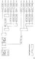
- FIG. 2 shows a block diagram for the implementation of the coupling and the counting function.
- the control input SET either the value NPS or the value Q is supplied to the input of the OWM 32 and stored in the OWM with a switching pulse CLK. It is therefore also available at the output of the OWM as the current count value APS. This is used as the address for the content of the RAM 31.
- a 12-bit word can be loaded in RAM for each of the 2 ⁇ 12 addresses. The word belonging to the respective address with the value N becomes effective as the next count value when it is switched through to the OWM input, because it is present at the RAM input after the next clock CLK.
- the counter is programmed to have 3 Passes through counted values.
- Figure 3 shows 3 cases in which the counter 2 immediately scans the user channel 11, 12, 13.
- the counter 2 scans a VC in which the user channel is located, a third counter is required to scan it is controlled by counter 2 in the same way becomes like counter 2 from counter 1.
- the system can therefore be arranged in the sense of the task be mastered.
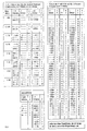
- FIG. 4 shows a table with all in System occurring patterns in which control bits C, c, Darning positions S, s and fixed information bits I occur. All positions that none of the above Properties assigned are marked with a period characterized. This is the table of I-C-S patterns. From this, the patterns with control bits (C, c) and the Patterns with I bits and stuffing positions (I, S, s) separated become. These are shown in special columns and numbered, as well as in another table after their Numbering compiled.
- a circuit structure according to the invention for generating a Bit stream in which all I bits excluding all bits not belonging to the user channel are collected shows Figure 5.
- the from the counter 5 and the assigned RAM existing control module 19 is the last in a chain of 2 or 3 such control modules. It runs through all byte positions the block from which the user bitstream is obtained becomes.
- a first task is to recognize the assignment of the tamping positions with the help of the control bits.
- all bytes containing control bits are fed to an M logic 12 via a C logic 11 specified in more detail in FIG.
- the switching mechanism controls the C logic in such a way that the maximum of 2 C bits per byte are supplied from their position in the byte to the two inputs of the M logic 12.
- the M logic is therefore programmed according to the case at hand.
- a second task consists of selecting the I bits the STM byte stream.
- the control module delivers 19 a code for the pattern for each byte position the bit position with I and S bits (I / S patterns) ROM 13 and also reports the number N of I bits in each Byte.
- the F logic 14 supplies the bit group for this via a U logic specified in more detail in FIG. 8 15 to a preferably 15 bit OWM 16 below Controlled by a ROM 17 and an OWM 18 existing adder, its function in Figure 9 in more detail is described.
- the adder keeps track of the filling level of the OWM 16 by storing the current level (U) and Addition of the size N of the bit group to be added.
Landscapes
- Engineering & Computer Science (AREA)
- Computer Networks & Wireless Communication (AREA)
- Signal Processing (AREA)
- Time-Division Multiplex Systems (AREA)
- Computer And Data Communications (AREA)
Description
| 1 | 2 | 3 | 4 | 5 | 6 | 7 | 8 | 9 |
| 0001 A1 | 0271 S | 0541 S | 0811 P | 1081 S | 1351 S | 1621 S | 1891 S | 2161 S |
| 0002 A1 | 0272 S | 0542 S | 0812 P | 1082 S | 1352 S | 1622 S | 1892 S | 2162 S |
| 0003 A1 | 0273 S | 0543 S | 0813 P | 1083 S | 1353 S | 1623 S | 1893 S | 2163 S |
| 0004 A2 | 0274 S | 0544 S | 0814 P | 1084 S | 1354 S | 1624 S | 1894 S | 2164 S |
| 0005 A2 | 0275 S | 0545 S | 0815 P | 1085 S | 1355 S | 1625 S | 1895 S | 2165 S |
| 0006 A2 | 0276 S | 0546 S | 0816 P | 1086 S | 1356 S | 1626 S | 1896 S | 2166 S |
| 0007 S | 0277 S | 0547 S | 0817 C- | 1087 S | 1357 S | 1627 S | 1897 S | 2167 S |
| 0008 S | 0278 S | 0548 S | 0818 C- | 1088 S | 135B S | 1628 S | 1898 S | 2168 S |
| 0009 S | 0279 S | 0549 S | 0819 C- | 1009 S | 1359 S | 1629 S | 1899 S | 2169 S |
| 0010 C | 0280 C | 0550 C | 0820 C+ | 1090 C | 1360 C | 1630 C | 1900 C | 2170 C |
| 0011 C | 0281 C | 0551 C | 0821 C+ | 1091 C | 1361 C | 1631 C | 1901 C | 2171 C |
| 0012 C | 0282 C | 0552 C | 0822 C+ | 1092 C | 1362 C | 1632 C | 1902 C | 2172 C |
| 0268 C | 0538 C | 0808 C | 1078 C | 1348 C | 1618 C | 1888 C | 2158 C | 2429 C |
| 0269 C | 0539 C | 0809 C | 1079 C | 1349 C | 1619 C | 1889 C | 2159 C | 2428 C |
| 0270 C | 0540 C | 0810 C | 1080 C | 1350 C | 1620 C | 1890 C | 2160 C | 2430 C |
| 1 | 2 | 3 | 4 | 5 | 6 | 7 | 8 | 9 |
| 0001 A1 | 0271 S | 0541 S | 0811 PA | 1081 S | 1351 S | 1621 S | 1891 S | 2161 S |
| 0003 A1 | 0272 S | 0542 S | 0812 PB | 1082 S | 1352 S | 1622 S | 1892 S | 2162 S |
| 0003 A1 | 0273 S | 0543 S | 0813 PC | 1083 S | 1353 S | 1623 S | 1893 S | 2163 S |
| 0004 A2 | 0274 S | 0544 S | 0814 PA | 1084 S | 1354 S | 1624 S | 1894 S | 2164 S |
| 0005 A2 | 0275 S | 0545 S | 0815 PB | 1085 S | 1355 S | 1625 S | 1895 S | 2165 S |
| 0006 A2 | 0276 S | 0546 S | 0816 PC | 1006 S | 1356 S | 1626 S | 1896 S | 2166 S |
| 0007 S | 0277 S | 0547 S | 0817 A- | 1087 S | 1357 S | 1627 S | 1897 S | 2167 S |
| 0008 S | 0278 S | 0548 S | 0818 D- | 1088 S | 1358 S | 1628 S | 1898 S | 2168 S |
| 0010 A | 0280 A | 0550 A | 0820 A+ | 1090 A | 1360 A | 1630 A | 1900 A | 2170 A |
| 0011 B | 0281 B | 0551 B | 0821 A+ | 1091 B | 1361 B | 1631 B | 1901 B | 2171 B |
| 0012 C | 0282 C | 0552 C | 0822 A+ | 1092 C | 1362 C | 1632 C | 1902 C | 2172 C |
| 0268 A | 0538 A | 0808 A | 1078 A | 1348 A | 1618 A | 1888 A | 2158 A | 2428 A |
| 0269 B | 0539 B | 0809 B | 1079 B | 1349 B | 1619 B | 1889 B | 2159 B | 2429 B |
| 0270 C | 0540 C | 0810 C | 1080 C | 1350 C | 1620 C | 1890 C | 2160 C | 2430 C |
| 0001 POH | 0262 POH | 0523 POH | 0784 POH | 1045 POH | 1306 POH | 1567 POH | 1828 POH | 2089 POH |
| 0002 C | 0263 C | 0524 C | 0785 C | 1046 C | 1307 C | 1568 C | 1829 C | 2090 C |
| 0003 C | 0264 C | 0525 C | 0786 C | 1047 C | 1308 C | 1569 C | 1830 C | 2091 C |
| 0261 C | 0522 C | 0783 C | 1044 C | 1305 C | 1566 C | 1827 C | 2088 C | 2349 C |
| 0001 POH | 0088 POH | 0175 POH | 0262 POH | 0349 POH | 0436 POH | 0523 POH | 0610 POH | 0697 POH |
| 0002 C | 0089 C | 0176 C | 0263 C | 0350 C | 0437 C | 0524 C | 0611 C | 0698 C |
| 0003 C | 0090 C | 0177 C | 0264 C | 0351 C | 0438 C | 0528 C | 0612 C | 0699 C |
| 0087 C | 0174 C | 0261 C | 0348 C | 0435 C | 0522 C | 0609 C | 0696 C | 0783 C |
| 0001 POH | 0262 POH | 0523 POH | 0784 POH | 1045 POH | 1306 POH | 1567 POH | 1820 POH | 2089 POH |
| 0002 * | 0263 * | 0524 * | 0785 * | 1046 * | 1307 * | 1568 * | 1829 * | 2090 * |
| 0003 * | 0264 * | 0525 * | 0786 * | 1047 * | 1308 * | 1559 * | 1830 * | 2091 * |
| 0004 PA | 0265 PA | 0526 A- | 0787 * | 1048 * | 1309 * | 1570 * | 1831 * | 2092 * |
| 0005 PB | 0266 PB | 0527 B- | 0788 * | 1049 * | 1310 * | 1571 * | 1832 * | 2093 * |
| 0006 PC | 0267 PC | 0528 C- | 0789 * | 1050 * | 1311 * | 1572 * | 1833 * | 2094 * |
| 0007 A | 0268 A | 0529 A+ | 0790 A | 1051 A | 1312 A | 1573 A | 1834 A | 2095 A |
| 0008 B | 0269 B | 0530 B+ | 0791 D | 1052 B | 1313 B | 1574 B | 1835 B | 2096 B |
| 0009 C | 0270 C | 0531 C+ | 0792 C | 1053 C | 1314 C | 1575 C | 1836 C | 2097 C |
| 0259 A | 0520 A | 0781 A | 1042 A | 1303 A | 1564 A | 1825 A | 2086 A | 2347 A |
| 0260 B | 0521 B | 0782 B | 1043 B | 1304 B | 1565 B | 1826 B | 2087 B | 2348 B |
| 0261 C | 0522 C | 0783 C | 1044 C | 1305 C | 1566 C | 1827 C | 2088 C | 2349 C |
| 0001 POH | 0086 POH | 0171 POH | 0256 POH | 0341 POH | 0426 POH | 0511 POH | 0596 POH | 0681 POH |
| 0002 C | 0087 C | 0172 C | 0257 C | 0342 C | 0427 C | 0512 C | 0597 C | 0682 C |
| 0003 C | 0088 C | 0173 C | 0258 C | 0343 C | 0428 C | 0513 C | 0598 C | 0683 C |
| 0085 C | 0170 C | 0255 C | 0340 C | 0425 C | 0510 C | 0595 C | 0680 C | 0765 C |


In Figur 1 ist die Funktion einer erfindungsgemäßen Anordnung anhand der Funktion der Steuerstufe für die STM-1 Ebene und in Bezug auf die darunter liegende Hierarchieebene dargestellt. Ein nicht weiter aufgeschlüsselter STM Byte Former (SBF) empfängt den STM-1 Bitstrom, überwacht ihn in bezug auf das Synchronwort, gibt nach dem letzten Byte des 6 Byte langen Synchronworts einen Synchron-Impuls ab und wandelt dann den Bitstrom in eine Bytefolge. Jedes gültige Byte wird mit einem Byte-Takt gekennzeichnet.
Dabei steuert das Schaltwerk die C-Logik so, daß die maximal 2 C-Bits pro Byte aus ihrer Position im Byte an die beiden Eingänge der M-Logik 12 geliefert werden. Es gibt Blockformate, in denen gleichzeitig 2 Stopfpositionen behandelt werden, so daß auch gleichzeitig 2 Folgen von C-Bits (C, c) beobachtet werden müssen. Bei Blockformaten mit nur einem gleichzeitig zu bearbeitenden Stopfbit gibt es andrerseits Bytes, in denen 2 Control Bits vorkommen. Die M-Logik wird deshalb entsprechend dem jeweils vorliegenden Fall programmiert. Sie zählt für 1 oder 2 Stopfbits die C-Bits mit Inhalt 1 und entscheidet über die Majorität bei 3 oder 5 C-Bits. Wenn für C oder c mehr Einsen als Nullen vorliegen, meldet die M-Logik für das mit C verknüpfte Stopfbit M=1 bzw. für das mit c verknüpfte Stopfbit m=1. Dies bedeutet, daß die Stopfposition nicht mit einem I-Bit belegt ist, sonst meldet die M-Logik M=0 bzw. m=0 zur Kennzeichnung einer mit einem 1-Bit belegten Stopfposition.
Claims (3)
- Decoder für Informationsströme in einem Synchronen Digitalen Nachrichten Transport System; das so ausgestaltet ist; daß die Informationsströme mehrerer Nachrichtenkanäle in einem Synchronen Transportmodul STM untergebracht werden können, in den Nachrichtenkanäle mit Hilfe von Virtuellen Containern VC definiert werden, und zwar innerhalb eines hierarchischen Systems von Blockformaten, bei dem Blockformate einer Hierarchie-Ebene als Träger für Blockformate der nächst niedrigen Ebene dienen; wobeiwobei der Decoderdas jeweilige Trägerformat einen Overhead enthält und ein oder mehrere Blockformate der nächst niedrigeren Ebene mit sich führt;ein mitgeführtes Blockformat auch über mehrere aufeinanderfolgende Synchrone Transportmodule STM verteilt sein kann;das Trägerformat für jedes mitgeführte Blockformat einen Pointer und eine Position bereitstellt, die mit einem Byte oder Tribyte belegt ist und leergelassen werden kann;der Pointer die Byteposition in seinem Blockformat definiert, wo das Format des betreffenden mitgeführten Blocks beginnt;der Wert eines Pointers inkrementiert oder dekrementiert werden kann und beim Dekrementieren die dafür vorgesehene Position zusätzlich belegt wird, beim Inkrementieren die dafür vorgesehene vorher belegte Position leerbleibt;das Blockformat der untersten Hierarchiestufe einen Virtual Container VC enthält, der Bit-Stopfpositionen aufweist, deren Zugehörigkeit zum User-Bitstrom von Control Bits definiert werden;der Informationsstrom in dem Synchronen Transportmodul STM in einem Bitstrom übertragen wird,- den Bitstrom mit Hilfe eines im Synchronen Transportmodul STM vorhandenen Synchronwortes in eine Bytefolge wandelt;- in Kette geschaltete Zähler (1), (3) zum Decodieren je eines Blockformats aufweist, die derart ausgestaltet sind, däß sie für jede Position einen eindeutigen Zustand definieren;- einen steuerbaren Modul (6) zur Entnahme von im Trägerformat fest positionierten Bytes aus dem STM-Bytestrom aufweist;- einen steuerbaren Modul (7) zur Entnahme von Pointerbytes, zur Ermittlung des Pointerwerts sowie von Pointeraktionen und zum Setzen des in der Kette folgenden Zählers auf den Pointerwert aufweist;- einen steuerbaren Modul (8) zur Freigabe eines Zählimpulses für den folgenden Zähler aufweist;- einen in der Kette letzten Zähler (5) aufweist zur Decodierung eines Virtual Containers und mit diesem Zähler verbundene steuerbare Module zur Entnahme von Bytes aus der STM-Bytefolge;- einen Modul (11) zur Entnahme von Bytes mit Control Bits und einen Modul (14) zur Entnahme von Bytes mit zum User-Kanal gehörenden Bits aufweist, und der Dekoder dadurch gekennzeichnet, ist daß jeder Zähler jedes Byte des in seiner Stufe vorhandenen Blockformats markiert, jedem Zähler, dem in der Kette ein weiterer folgt, ein programmierbarer Speicher (RAM 2, 4) zugeordnet ist, der abhängig vom Zählerstand einen Steuercode an den Modul (6) zur Entnahme von im Trägerformat fest positionierten Bytes aus dem STM-Bytestrom an den Modul (7) zur Entnahme von Pointerbytes zur Ermittlung des Pointerwerts und zur Ermittlung der Pointeraktion oder an den Modul (8) zur Freigabe eines Zählimpulses für den in der Kette folgenden Zähler abgibt, und dem letzten Zähler in der Kette (5) ein programmierbarer Speicher (RAM) zugeordnet ist, der zur Entnahme von Bytes aus dem zu decodierenden Virtual Container abhängig vom Zählerstand einen Steuercode an den Modul (11) zur Entnahme von Bytes mit Control Bits oder an den Modul (14) zur Entnahme von Bytes mit zum User-Kanal gehörenden Bits abgibt.
- Decoder nach Anspruch 1, gekennzeichnet durch einen steuerbaren F-Logik-Modul (14) zum Anreihen aller User Info Bits (I-Bits) eines STM-Bytes und durch einen steuerbaren U-Logik Modul (15) zum Verschieben der Einkopplung der so gewonnen I-Bit-Gruppen in ein 15 Bit breites OWM (16), das an seinem Ausgang 8 Bit breite User Bytes abgibt in deren Folge der I-Bit-Strom lückenlos vorliegt; wobei der U-Logik-Modul (15) von einem Addierer (17, 18) einen Wert U erhält, der die Einkoppelstelle für das OWM (16) definiert, wobei die ersten 8 Bits des OWM (16) den Bereich des anzukoppelnden User Bytes darstellen, wobei der Addierer (17, 18) bei Vorliegen eines kompletten User Byters ein Valid-Signal (V) abgibt, und der U-Logik-Modul (15) mit dem nächsten Einkoppeltakt einen nicht mehr in das gemeldete Byte passenden Bitgruppenrest wieder in das OWM (16) an den Anfang des nächsten U-Bytes lädt.
- Decoder nach Anspruch 2, gekennzeichnet durch eine Anordnung aus einem ersten ROM (13), einem zweiten ROM (17) und einem OWM (18), wobei ein programmierbares RAM ein das Pattern des STM-Bytes mit Info- und Stopfbits kennzeichnender Code (I) von der Majoritätslogik (12) die aus den Control Bits C, c gewonnen Ergebnisse M, m dem Adresseingang des ersten ROM vom Positionszähler (5) zuführt, wobei das erste ROM (13) aus dem Code I und den Werten M, m einen Code F zum Steuern der F-Logik (14) ermittelt und das Increment N für den Wert U entsprechend der Zahl der einzukoppelnden 1-Bits bildet, wobei das OWM (18) den jeweils aktuellen Wert U speichert, der die Einkoppelstelle für das OWM (16) definiert, wobei das zweite ROM (17) aus den zugeführten Werten N und U den nächsten Einkoppelwert für das OWM (18) bildet.
Applications Claiming Priority (2)
| Application Number | Priority Date | Filing Date | Title |
|---|---|---|---|
| DE4205238 | 1992-02-21 | ||
| DE19924205238 DE4205238C1 (de) | 1992-02-21 | 1992-02-21 |
Publications (3)
| Publication Number | Publication Date |
|---|---|
| EP0563511A2 EP0563511A2 (de) | 1993-10-06 |
| EP0563511A3 EP0563511A3 (en) | 1996-03-13 |
| EP0563511B1 true EP0563511B1 (de) | 2001-05-09 |
Family
ID=6452213
Family Applications (1)
| Application Number | Title | Priority Date | Filing Date |
|---|---|---|---|
| EP19930100460 Expired - Lifetime EP0563511B1 (de) | 1992-02-21 | 1993-01-14 | Decoder für Informationsströme in einem synchronen digitalen Nachrichten-Transportsystem |
Country Status (3)
| Country | Link |
|---|---|
| EP (1) | EP0563511B1 (de) |
| JP (1) | JPH0621911A (de) |
| DE (1) | DE4205238C1 (de) |
Families Citing this family (5)
| Publication number | Priority date | Publication date | Assignee | Title |
|---|---|---|---|---|
| JP2648711B2 (ja) * | 1986-11-07 | 1997-09-03 | 株式会社 ペトカ | ピッチ系炭素繊維三次元織物の製造法 |
| FI93287C (fi) * | 1993-03-16 | 1995-03-10 | Nokia Telecommunications Oy | Menetelmä toisiinsa kytkettyjen SDH- ja PDH-tietoliikenneverkkojen synkronoimiseksi |
| FI93289C (fi) * | 1993-03-16 | 1995-03-10 | Nokia Telecommunications Oy | Menetelmä ehdollisten kytkentöjen ohjaamiseksi synkronisessa digitaalisessa tietoliikennejärjestelmässä |
| FI93288C (fi) * | 1993-03-16 | 1995-03-10 | Nokia Telecommunications Oy | Menetelmä ehdollisten kytkentöjen ohjaamiseksi tietoliikennejärjestelmässä |
| JPH08102747A (ja) * | 1994-09-30 | 1996-04-16 | Toshiba Corp | 通信用lsi |
Family Cites Families (2)
| Publication number | Priority date | Publication date | Assignee | Title |
|---|---|---|---|---|
| DE4018687A1 (de) * | 1989-07-18 | 1991-01-31 | Siemens Ag | Verfahren und anordnung zur uebertragung eines blocks aus vier verwaltungseinheiten au-31 oder aus drei verwaltungseinheiten au-32 in einem synchronen transport-modul stm-1 |
| FR2657741B1 (fr) * | 1990-01-29 | 1992-04-03 | Cit Alcatel | Interface de restructuration de trames pour trains numeriques multiplexes par multiplexage temporel d'affluents numeriques a differents debits. |
-
1992
- 1992-02-21 DE DE19924205238 patent/DE4205238C1/de not_active Expired - Fee Related
-
1993
- 1993-01-14 EP EP19930100460 patent/EP0563511B1/de not_active Expired - Lifetime
- 1993-02-22 JP JP5031710A patent/JPH0621911A/ja active Pending
Also Published As
| Publication number | Publication date |
|---|---|
| DE4205238C1 (de) | 1993-01-07 |
| JPH0621911A (ja) | 1994-01-28 |
| EP0563511A3 (en) | 1996-03-13 |
| EP0563511A2 (de) | 1993-10-06 |
Similar Documents
| Publication | Publication Date | Title |
|---|---|---|
| EP0422443B1 (de) | Multiplexer und Demultiplexer, insbesondere für Nachrichtenübertragungs-Netze mit einer synchronen Hierarchie der Digitalsignale | |
| EP0429888B1 (de) | Verfahren zur Übertragung eines digitalen Breitbandsignals in einer Untersystemeinheitenkette über ein Netz einer Synchron-Digital-Multiplexhierarchie | |
| EP1158710B1 (de) | Verfahren zum Übertragen von synchronen Transportmodulen über ein synchrones Transportnetz | |
| DE69836157T2 (de) | Verfahren und Vorrichtung zum Demultiplexen digitaler Signalströme | |
| DE60213430T2 (de) | Stm-1 bis stm-64 sdh/sonet rahmenanpasser mit datenmultiplexen aus einer serie von konfigurierbaren e/a ports | |
| EP0507385A2 (de) | Übertragungssystem für die synchrone digitale Hierarchie | |
| EP0475498B1 (de) | Schaltungsanordnung zur Bitratenanpassung zweier digitaler Signale | |
| EP0639903A2 (de) | Übertragungssystem | |
| EP1051057A2 (de) | Transport von verknüpften Containern in einem synchronen Nachrichtenübertragungsnetz | |
| DE2825954C2 (de) | Digitale Zeitmultiplexanlage | |
| EP0598455B1 (de) | Übertragungssystem der synchronen digitalen Hierarchie | |
| EP0563511B1 (de) | Decoder für Informationsströme in einem synchronen digitalen Nachrichten-Transportsystem | |
| EP1083693B1 (de) | Verfahren und Vorrichtung zum Umwandeln eines SONET-Signals in ein SDH-Signal | |
| DE60320266T2 (de) | Synchroner übertragungsnetzknoten | |
| EP0415112B1 (de) | Kreuzschaltungsverfahren (Cross-Connect) für STM-1-Signale der Synchron-Digital-Multiplexhierarchie | |
| DE10047510A1 (de) | Transportmodul für SDH/SONET | |
| DE19627728A1 (de) | Netzelement und Ein-/Ausgabeeinheit für ein synchrones Übertragungssystem | |
| EP0006986B1 (de) | Datenübertragungssystem sowie Verfahren und Schaltungsanordnung zum Betreiben eines solchen Datenübertragunssystems | |
| EP0597349B1 (de) | Verfahren und Anordnung zur Rückgewinnung von in Funktionsdatenblöcken übertragenen plesiochronen Signalen | |
| EP0491064A1 (de) | Verfahren und Anordnung zum Teilen der Frequenz einer Wechselspannung mit einem nicht ganzzahligen Teilungsfaktor | |
| EP0993711B1 (de) | Verfahren und schaltungsanordnung zur adaption und durchschaltung eines datenstromes | |
| EP0434629A2 (de) | Verfahren und Anordnung zur Verarbeitung von Signalisierinformation in konfigurierbaren Multiplexern | |
| DE19608621C2 (de) | Telekommunikationsnetzwerk | |
| DE69829505T2 (de) | Einfügung einer mehrzahl virtueller container höherer ordnung in einen stm rahmen höherer ordnung innerhalb eines sdh systems | |
| DE4218207A1 (de) | Verfahren und Anordnung zum Transport vorgegebener Overhead-Bytes in einem Netzknoten der Synchron-Digital-Hierarchie |
Legal Events
| Date | Code | Title | Description |
|---|---|---|---|
| PUAI | Public reference made under article 153(3) epc to a published international application that has entered the european phase |
Free format text: ORIGINAL CODE: 0009012 |
|
| AK | Designated contracting states |
Kind code of ref document: A2 Designated state(s): DK FR GB IT |
|
| PUAL | Search report despatched |
Free format text: ORIGINAL CODE: 0009013 |
|
| AK | Designated contracting states |
Kind code of ref document: A3 Designated state(s): DK FR GB IT |
|
| 17P | Request for examination filed |
Effective date: 19960406 |
|
| 17Q | First examination report despatched |
Effective date: 19980706 |
|
| GRAG | Despatch of communication of intention to grant |
Free format text: ORIGINAL CODE: EPIDOS AGRA |
|
| RIC1 | Information provided on ipc code assigned before grant |
Free format text: 7H 04Q 11/04 A, 7H 04J 3/16 B |
|
| GRAG | Despatch of communication of intention to grant |
Free format text: ORIGINAL CODE: EPIDOS AGRA |
|
| GRAG | Despatch of communication of intention to grant |
Free format text: ORIGINAL CODE: EPIDOS AGRA |
|
| GRAH | Despatch of communication of intention to grant a patent |
Free format text: ORIGINAL CODE: EPIDOS IGRA |
|
| RIN1 | Information on inventor provided before grant (corrected) |
Inventor name: HEIDENREICH, KARL-HEINZ, DIPL.-ING. |
|
| GRAH | Despatch of communication of intention to grant a patent |
Free format text: ORIGINAL CODE: EPIDOS IGRA |
|
| GRAA | (expected) grant |
Free format text: ORIGINAL CODE: 0009210 |
|
| AK | Designated contracting states |
Kind code of ref document: B1 Designated state(s): DK FR GB IT |
|
| RAP2 | Party data changed (patent owner data changed or rights of a patent transferred) |
Owner name: ACTERNA ENINGEN GMBH |
|
| ITF | It: translation for a ep patent filed |
Owner name: BUGNION S.P.A. |
|
| PG25 | Lapsed in a contracting state [announced via postgrant information from national office to epo] |
Ref country code: DK Free format text: LAPSE BECAUSE OF FAILURE TO SUBMIT A TRANSLATION OF THE DESCRIPTION OR TO PAY THE FEE WITHIN THE PRESCRIBED TIME-LIMIT Effective date: 20010809 |
|
| GBT | Gb: translation of ep patent filed (gb section 77(6)(a)/1977) |
Effective date: 20010816 |
|
| ET | Fr: translation filed | ||
| PGFP | Annual fee paid to national office [announced via postgrant information from national office to epo] |
Ref country code: GB Payment date: 20011217 Year of fee payment: 10 |
|
| PGFP | Annual fee paid to national office [announced via postgrant information from national office to epo] |
Ref country code: FR Payment date: 20011218 Year of fee payment: 10 |
|
| REG | Reference to a national code |
Ref country code: GB Ref legal event code: IF02 |
|
| PLBE | No opposition filed within time limit |
Free format text: ORIGINAL CODE: 0009261 |
|
| STAA | Information on the status of an ep patent application or granted ep patent |
Free format text: STATUS: NO OPPOSITION FILED WITHIN TIME LIMIT |
|
| 26N | No opposition filed | ||
| PG25 | Lapsed in a contracting state [announced via postgrant information from national office to epo] |
Ref country code: GB Free format text: LAPSE BECAUSE OF NON-PAYMENT OF DUE FEES Effective date: 20030114 |
|
| GBPC | Gb: european patent ceased through non-payment of renewal fee | ||
| PG25 | Lapsed in a contracting state [announced via postgrant information from national office to epo] |
Ref country code: FR Free format text: LAPSE BECAUSE OF NON-PAYMENT OF DUE FEES Effective date: 20030930 |
|
| REG | Reference to a national code |
Ref country code: FR Ref legal event code: ST |
|
| PG25 | Lapsed in a contracting state [announced via postgrant information from national office to epo] |
Ref country code: IT Free format text: LAPSE BECAUSE OF NON-PAYMENT OF DUE FEES;WARNING: LAPSES OF ITALIAN PATENTS WITH EFFECTIVE DATE BEFORE 2007 MAY HAVE OCCURRED AT ANY TIME BEFORE 2007. THE CORRECT EFFECTIVE DATE MAY BE DIFFERENT FROM THE ONE RECORDED. Effective date: 20050114 |