EP0560261B1 - Vorrichtung zum Festlegen von Schaltungsplatinen in einem Gerätegehäuse - Google Patents
Vorrichtung zum Festlegen von Schaltungsplatinen in einem Gerätegehäuse Download PDFInfo
- Publication number
- EP0560261B1 EP0560261B1 EP93103690A EP93103690A EP0560261B1 EP 0560261 B1 EP0560261 B1 EP 0560261B1 EP 93103690 A EP93103690 A EP 93103690A EP 93103690 A EP93103690 A EP 93103690A EP 0560261 B1 EP0560261 B1 EP 0560261B1
- Authority
- EP
- European Patent Office
- Prior art keywords
- housing
- spring
- bracket
- flanges
- circuit boards
- Prior art date
- Legal status (The legal status is an assumption and is not a legal conclusion. Google has not performed a legal analysis and makes no representation as to the accuracy of the status listed.)
- Expired - Lifetime
Links
Images

Classifications
-
- H—ELECTRICITY
- H05—ELECTRIC TECHNIQUES NOT OTHERWISE PROVIDED FOR
- H05K—PRINTED CIRCUITS; CASINGS OR CONSTRUCTIONAL DETAILS OF ELECTRIC APPARATUS; MANUFACTURE OF ASSEMBLAGES OF ELECTRICAL COMPONENTS
- H05K7/00—Constructional details common to different types of electric apparatus
- H05K7/14—Mounting supporting structure in casing or on frame or rack
- H05K7/1401—Mounting supporting structure in casing or on frame or rack comprising clamping or extracting means
- H05K7/1402—Mounting supporting structure in casing or on frame or rack comprising clamping or extracting means for securing or extracting printed circuit boards
- H05K7/1408—Mounting supporting structure in casing or on frame or rack comprising clamping or extracting means for securing or extracting printed circuit boards by a unique member which latches several boards, e.g. locking bars
Definitions
- the invention relates to a device for fixing a plurality of circuit boards in a device housing, the circuit boards each being connected at one of their edges to a strip-shaped metal diaphragm directed perpendicular to the plane of the board, each of which has a right-angled flange at one of its longitudinal ends, and wherein the circuit boards can be inserted into the housing parallel to one another in such a way that the metal covers on the one hand and their flanges on the other are each in one plane.
- the electronic circuit boards or plug-in cards are connected to the edge cards Central processor (CPU) connected.
- CPU Central processor
- the interfaces (usually D-sub sockets) to the respective plug connection to the plug-in card are located on one of the above-mentioned metal panels, which in turn is connected to the device housing with a screw in a metallically conductive manner.
- the invention has for its object to provide an easy and safe to use device of the type mentioned, with which the plug-in cards and panels can be reliably fixed while ensuring electrical contact between the metal panels and the housing.
- a metal retaining bracket which extends between the housing walls directed parallel to the circuit boards perpendicular to the latter and extends over the flanges of the metal panels, can be connected to the housing in a positive and / or non-positive manner and is intended for bearing against the individual flanges Has spring elements.
- the retaining bracket is formed by a U-shaped rail made of spring steel, from whose U-transverse web intended for abutment on the flanges, spring tongues are punched out, which are bent obliquely outward from the plane of the U-transverse web in the open state of the retaining bracket.
- the spring elements are pressed back into the plane of the U-crossbar, scraping along the surface of the flanges and thereby creating reliable electrical contact between the bracket and the metal covers.
- the bracket By simply pulling the handle section of the spring clip, the bracket can be released again.
- the spring tongues are preferably punched out in such a way that their free ends point away from the longitudinal end of the holding bracket provided with the tongue. This causes the spring tongues to scrape along the flanges of the metal panels when the holding bracket is pivoted and to dig into the material.
- the holding bracket 10 shown in FIGS. 1 and 2 essentially consists of a U-shaped rail 12 made of spring steel with U-legs 14 and a U-cross bar 16. At one longitudinal end, the U-cross bar 16 has a tongue 18 formed integrally with it At its opposite end, an extension section of the U-cross bar 16 is bent into a spring clip 20. This includes a first spring leg 22, which is bent perpendicularly from the U-crosspiece 16 to the opposite side to the direction of extension of the U-leg 14, and a U-shaped bent back, compared to the spring leg 22 longer second spring leg 24, one at its free end has angled handle portion 26.
- Pairs of spring tongues 28 are punched out of the U-cross bar 16 and are angled outward from the plane of the U-cross leg 16, as can be seen in FIG. 2.
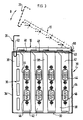
- FIG. 3 schematically shows a device housing 30 for receiving electronic circuit boards (not shown).
- the housing 30 comprises a base 32, side walls 34 and a grid-shaped rear wall 36, which in the present example is connected to the base 32 and comprises a number of struts 38 which are oriented parallel to the side walls 34 and which on their side Bottom 32 far end are interconnected by a web 40 bent outward at right angles.
- the circuit boards, not shown, are inserted into this housing in such a way that they are directed parallel to the side walls 34.
- a metal screen 42 is connected to each of the circuit boards via edge connectors, the surface of which is directed perpendicular to the plane of the respective circuit board.
- the metal panels 42 each carry plugs 44, 46 for connecting the circuit boards to other parts of the device or external devices.
- the arrangement of the circuit boards in the device housing 30 is such that the panels 42 with their plugs 44, 46 lie in the gaps between two struts 38 of the rear wall 36.
- the panels 42 each have a right-angled flange 48 which rests on the web 40 of the rear wall 36 when the plug-in card is fully inserted. So far, this flange 48 has been screwed to the web 40.
- the metal screens 42 and thus also the plug-in cards are fixed in the housing 30 with the aid of the holding bracket 10 described with reference to FIGS. 1 and 2. This is shown in FIG. 3 by solid lines in its closed position and by Dashed lines shown in an open position.
- the retaining bracket is inserted with the tongue 18 into a slot 50 of the right side wall 34 in FIG.
- bracket 10 can then be pivoted in the direction of the double arrow B in FIG. 3.
- this is pressed down against the flanges 48 of the metal panels 42, the spring tongues 28 being pressed back into the plane of the U-crosspiece 16 of the bracket 10 and thereby dig into the material of the flanges 48.
- the securing bracket 10 in the closed position shown by solid lines is done by inserting the spring clip 20 into a recess 52 in the web 40 of the housing rear wall 36. The spring legs of the spring clip 20 are compressed so that they are under pressure at the edges of the recess 52 rest and thus secure the bracket 10 in the closed position.
- the holding bracket 10 By simply pulling on the grip section 26, the holding bracket 10 can be pivoted away from the flanges 48 and the connection of the metal screens 42 to the housing 30 can thus be released. In this way, the replacement of plug-in cards can be done quickly and easily, without the risk that fasteners can fall into the device.
Landscapes
- Engineering & Computer Science (AREA)
- Microelectronics & Electronic Packaging (AREA)
- Casings For Electric Apparatus (AREA)
- Mounting Of Printed Circuit Boards And The Like (AREA)
- Multi-Conductor Connections (AREA)
Applications Claiming Priority (2)
| Application Number | Priority Date | Filing Date | Title |
|---|---|---|---|
| DE4207572A DE4207572C1 (enExample) | 1992-03-10 | 1992-03-10 | |
| DE4207572 | 1992-03-10 |
Publications (2)
| Publication Number | Publication Date |
|---|---|
| EP0560261A1 EP0560261A1 (de) | 1993-09-15 |
| EP0560261B1 true EP0560261B1 (de) | 1995-05-31 |
Family
ID=6453678
Family Applications (1)
| Application Number | Title | Priority Date | Filing Date |
|---|---|---|---|
| EP93103690A Expired - Lifetime EP0560261B1 (de) | 1992-03-10 | 1993-03-08 | Vorrichtung zum Festlegen von Schaltungsplatinen in einem Gerätegehäuse |
Country Status (3)
| Country | Link |
|---|---|
| EP (1) | EP0560261B1 (enExample) |
| DE (2) | DE4207572C1 (enExample) |
| ES (1) | ES2072782T3 (enExample) |
Families Citing this family (5)
| Publication number | Priority date | Publication date | Assignee | Title |
|---|---|---|---|---|
| DE4403907A1 (de) * | 1994-02-08 | 1995-08-10 | Vobis Microcomputer Ag | Personal-Computer mit einem Gehäuse, einer Hauptplatine, Steckkarten und einer Haltevorrichtung hierfür |
| FR2762500B1 (fr) * | 1997-04-23 | 1999-06-11 | Rodolphe Reisch | Meuble a racks |
| ES2169697B1 (es) * | 2000-11-03 | 2003-11-01 | Lear Automotive Eeds Spain | Dispositivo perfeccionado para fijacion de cajas de distribucion. |
| DE10064115C1 (de) * | 2000-12-21 | 2002-06-20 | Fujitsu Siemens Computers Gmbh | Anordnung zur Festlegung eines Slotwinkels |
| DE10209083C2 (de) * | 2002-03-01 | 2003-12-24 | Fujitsu Siemens Computers Gmbh | Anordnung zur Festlegung eines Slotwinkels |
Family Cites Families (4)
| Publication number | Priority date | Publication date | Assignee | Title |
|---|---|---|---|---|
| DE2757761A1 (de) * | 1977-12-23 | 1979-06-28 | Siemens Ag | Baugruppentraeger fuer elektronische baugruppen |
| CH667959A5 (en) * | 1985-07-26 | 1988-11-15 | Contraves Ag | Housing frame for electronic rack mounted circuit boards - has hinged front carrier unit that retains modules and provides handles for carrying |
| US5067041A (en) * | 1989-10-27 | 1991-11-19 | International Business Machines Corporation | Apparatus for reducing electromagnetic radiation from a computer device |
| DE9003253U1 (de) * | 1990-03-20 | 1991-08-01 | Siemens Nixdorf Informationssysteme AG, 4790 Paderborn | Halteeinrichtung für Steckkarten |
-
1992
- 1992-03-10 DE DE4207572A patent/DE4207572C1/de not_active Expired - Fee Related
-
1993
- 1993-03-08 DE DE59300225T patent/DE59300225D1/de not_active Expired - Fee Related
- 1993-03-08 ES ES93103690T patent/ES2072782T3/es not_active Expired - Lifetime
- 1993-03-08 EP EP93103690A patent/EP0560261B1/de not_active Expired - Lifetime
Also Published As
| Publication number | Publication date |
|---|---|
| ES2072782T3 (es) | 1995-07-16 |
| DE59300225D1 (de) | 1995-07-06 |
| EP0560261A1 (de) | 1993-09-15 |
| DE4207572C1 (enExample) | 1993-07-22 |
Similar Documents
| Publication | Publication Date | Title |
|---|---|---|
| DE69320016T2 (de) | Kartenrandverbinder | |
| DE602005000149T2 (de) | Anschlussanordnung eines elektrischen Gerätes | |
| DE2925938A1 (de) | Elektrischer flachsteckverbinder | |
| EP0793313A2 (de) | Abgewinkelter Einpress-Steck-verbinder zum Einpressen in Bohrungen einer Leiterplatte | |
| DE2409075A1 (de) | Elektrischer verbinder | |
| EP0898327A2 (de) | Leiterplattensteckbuchse | |
| EP0735615A2 (de) | Anschlusselement für elektrische Geräte | |
| DE29602740U1 (de) | Elektrischer Steckverbinder | |
| DE2931441A1 (de) | Erdvorrichtung | |
| DE102009019699A1 (de) | Anschlussklemme für Leiterplatten | |
| EP0780923B1 (de) | Klemme zum Verbinden eines Leiterendes mit einem Kontakt | |
| DE69307103T2 (de) | Verfahren zur Befestigung eines beweglichen auf einen festen Verbinder und Befestigungsteil dafür | |
| EP0822337B1 (de) | Haltevorrichtung für elektrische Lüfter, insbesondere Kleinstlüfter | |
| EP0666524A2 (de) | Personal-Computer mit einem Gehäuse, einer Hauptplatine, Steckkarten und einer Haltevorrichtung hierfür | |
| DE4000548A1 (de) | Steckerleiste | |
| EP0560261B1 (de) | Vorrichtung zum Festlegen von Schaltungsplatinen in einem Gerätegehäuse | |
| DE4433735A1 (de) | Verschwenkbarer Verbinder für planare elektronische Vorrichtungen | |
| EP0433688A1 (de) | Vorrichtung zum elektrischen Kontaktieren einer längs einer ihrer Seiten Anschlusspole aufweisenden, elektronischen Karte, insbesondere IC-Memory-Karte, mit einer Basisleiterplatte | |
| DE7011611U (de) | Gabelfoermige kontaktfeder. | |
| DE19830878B4 (de) | Elektrische Verbindungsanordnung zwischen zwei elektrischen Bauelementen für ein elektrisches Bauteil | |
| DE102005046053B4 (de) | Elektrische Vorrichtung mit einer Leiterplatte und einem Bauteil | |
| DE2644612A1 (de) | Einrichtung zur begrenzung der rueckfederung von rastzungen an kontaktelementen mehrpoliger elektrischer steckverbinder | |
| DE19610610A1 (de) | Anordnung zur Verbindung eines elektrischen Leiters mit einem Schneidklemmkontakt | |
| DE29618628U1 (de) | Abgeschirmter Baugruppenträger | |
| EP0121720A2 (de) | Kontaktanordnung zur Herstellung eines elektrischen Kontaktes zwischen aneinandergrenzenden Gehäuseteilen |
Legal Events
| Date | Code | Title | Description |
|---|---|---|---|
| PUAI | Public reference made under article 153(3) epc to a published international application that has entered the european phase |
Free format text: ORIGINAL CODE: 0009012 |
|
| AK | Designated contracting states |
Kind code of ref document: A1 Designated state(s): DE ES FR GB IT |
|
| 17P | Request for examination filed |
Effective date: 19940216 |
|
| 17Q | First examination report despatched |
Effective date: 19940926 |
|
| GRAA | (expected) grant |
Free format text: ORIGINAL CODE: 0009210 |
|
| AK | Designated contracting states |
Kind code of ref document: B1 Designated state(s): DE ES FR GB IT |
|
| REF | Corresponds to: |
Ref document number: 59300225 Country of ref document: DE Date of ref document: 19950706 |
|
| REG | Reference to a national code |
Ref country code: ES Ref legal event code: FG2A Ref document number: 2072782 Country of ref document: ES Kind code of ref document: T3 |
|
| ITF | It: translation for a ep patent filed | ||
| ET | Fr: translation filed | ||
| GBT | Gb: translation of ep patent filed (gb section 77(6)(a)/1977) |
Effective date: 19950814 |
|
| PGFP | Annual fee paid to national office [announced via postgrant information from national office to epo] |
Ref country code: ES Payment date: 19960311 Year of fee payment: 4 |
|
| PLBE | No opposition filed within time limit |
Free format text: ORIGINAL CODE: 0009261 |
|
| PGFP | Annual fee paid to national office [announced via postgrant information from national office to epo] |
Ref country code: DE Payment date: 19960520 Year of fee payment: 4 |
|
| 26N | No opposition filed | ||
| PGFP | Annual fee paid to national office [announced via postgrant information from national office to epo] |
Ref country code: GB Payment date: 19970224 Year of fee payment: 5 |
|
| PG25 | Lapsed in a contracting state [announced via postgrant information from national office to epo] |
Ref country code: ES Free format text: LAPSE BECAUSE OF NON-PAYMENT OF DUE FEES Effective date: 19970310 |
|
| PGFP | Annual fee paid to national office [announced via postgrant information from national office to epo] |
Ref country code: FR Payment date: 19970321 Year of fee payment: 5 |
|
| PG25 | Lapsed in a contracting state [announced via postgrant information from national office to epo] |
Ref country code: DE Free format text: LAPSE BECAUSE OF NON-PAYMENT OF DUE FEES Effective date: 19980101 |
|
| PG25 | Lapsed in a contracting state [announced via postgrant information from national office to epo] |
Ref country code: GB Free format text: LAPSE BECAUSE OF NON-PAYMENT OF DUE FEES Effective date: 19980308 |
|
| PG25 | Lapsed in a contracting state [announced via postgrant information from national office to epo] |
Ref country code: FR Free format text: THE PATENT HAS BEEN ANNULLED BY A DECISION OF A NATIONAL AUTHORITY Effective date: 19980331 |
|
| GBPC | Gb: european patent ceased through non-payment of renewal fee |
Effective date: 19980308 |
|
| REG | Reference to a national code |
Ref country code: FR Ref legal event code: ST |
|
| REG | Reference to a national code |
Ref country code: ES Ref legal event code: FD2A Effective date: 19990201 |
|
| PG25 | Lapsed in a contracting state [announced via postgrant information from national office to epo] |
Ref country code: IT Free format text: LAPSE BECAUSE OF NON-PAYMENT OF DUE FEES;WARNING: LAPSES OF ITALIAN PATENTS WITH EFFECTIVE DATE BEFORE 2007 MAY HAVE OCCURRED AT ANY TIME BEFORE 2007. THE CORRECT EFFECTIVE DATE MAY BE DIFFERENT FROM THE ONE RECORDED. Effective date: 20050308 |