EP0558712B2 - Elektrisches gerät, insbesondere schalt- und steuergerät für kraftfahrzeuge - Google Patents
Elektrisches gerät, insbesondere schalt- und steuergerät für kraftfahrzeuge Download PDFInfo
- Publication number
- EP0558712B2 EP0558712B2 EP92918773A EP92918773A EP0558712B2 EP 0558712 B2 EP0558712 B2 EP 0558712B2 EP 92918773 A EP92918773 A EP 92918773A EP 92918773 A EP92918773 A EP 92918773A EP 0558712 B2 EP0558712 B2 EP 0558712B2
- Authority
- EP
- European Patent Office
- Prior art keywords
- electrical device
- circuit board
- heat
- heat conductive
- printed circuit
- Prior art date
- Legal status (The legal status is an assumption and is not a legal conclusion. Google has not performed a legal analysis and makes no representation as to the accuracy of the status listed.)
- Expired - Lifetime
Links
Images
Classifications
-
- H—ELECTRICITY
- H05—ELECTRIC TECHNIQUES NOT OTHERWISE PROVIDED FOR
- H05K—PRINTED CIRCUITS; CASINGS OR CONSTRUCTIONAL DETAILS OF ELECTRIC APPARATUS; MANUFACTURE OF ASSEMBLAGES OF ELECTRICAL COMPONENTS
- H05K7/00—Constructional details common to different types of electric apparatus
- H05K7/20—Modifications to facilitate cooling, ventilating, or heating
- H05K7/20845—Modifications to facilitate cooling, ventilating, or heating for automotive electronic casings
- H05K7/20854—Heat transfer by conduction from internal heat source to heat radiating structure
-
- H—ELECTRICITY
- H05—ELECTRIC TECHNIQUES NOT OTHERWISE PROVIDED FOR
- H05K—PRINTED CIRCUITS; CASINGS OR CONSTRUCTIONAL DETAILS OF ELECTRIC APPARATUS; MANUFACTURE OF ASSEMBLAGES OF ELECTRICAL COMPONENTS
- H05K1/00—Printed circuits
- H05K1/02—Details
- H05K1/0201—Thermal arrangements, e.g. for cooling, heating or preventing overheating
- H05K1/0203—Cooling of mounted components
- H05K1/0209—External configuration of printed circuit board adapted for heat dissipation, e.g. lay-out of conductors, coatings
-
- H—ELECTRICITY
- H05—ELECTRIC TECHNIQUES NOT OTHERWISE PROVIDED FOR
- H05K—PRINTED CIRCUITS; CASINGS OR CONSTRUCTIONAL DETAILS OF ELECTRIC APPARATUS; MANUFACTURE OF ASSEMBLAGES OF ELECTRICAL COMPONENTS
- H05K7/00—Constructional details common to different types of electric apparatus
- H05K7/20—Modifications to facilitate cooling, ventilating, or heating
- H05K7/2089—Modifications to facilitate cooling, ventilating, or heating for power electronics, e.g. for inverters for controlling motor
- H05K7/209—Heat transfer by conduction from internal heat source to heat radiating structure
-
- H—ELECTRICITY
- H05—ELECTRIC TECHNIQUES NOT OTHERWISE PROVIDED FOR
- H05K—PRINTED CIRCUITS; CASINGS OR CONSTRUCTIONAL DETAILS OF ELECTRIC APPARATUS; MANUFACTURE OF ASSEMBLAGES OF ELECTRICAL COMPONENTS
- H05K1/00—Printed circuits
- H05K1/18—Printed circuits structurally associated with non-printed electric components
-
- H—ELECTRICITY
- H05—ELECTRIC TECHNIQUES NOT OTHERWISE PROVIDED FOR
- H05K—PRINTED CIRCUITS; CASINGS OR CONSTRUCTIONAL DETAILS OF ELECTRIC APPARATUS; MANUFACTURE OF ASSEMBLAGES OF ELECTRICAL COMPONENTS
- H05K2201/00—Indexing scheme relating to printed circuits covered by H05K1/00
- H05K2201/06—Thermal details
- H05K2201/066—Heatsink mounted on the surface of the printed circuit board [PCB]
-
- H—ELECTRICITY
- H05—ELECTRIC TECHNIQUES NOT OTHERWISE PROVIDED FOR
- H05K—PRINTED CIRCUITS; CASINGS OR CONSTRUCTIONAL DETAILS OF ELECTRIC APPARATUS; MANUFACTURE OF ASSEMBLAGES OF ELECTRICAL COMPONENTS
- H05K2201/00—Indexing scheme relating to printed circuits covered by H05K1/00
- H05K2201/09—Shape and layout
- H05K2201/09209—Shape and layout details of conductors
- H05K2201/0929—Conductive planes
- H05K2201/09354—Ground conductor along edge of main surface
-
- H—ELECTRICITY
- H05—ELECTRIC TECHNIQUES NOT OTHERWISE PROVIDED FOR
- H05K—PRINTED CIRCUITS; CASINGS OR CONSTRUCTIONAL DETAILS OF ELECTRIC APPARATUS; MANUFACTURE OF ASSEMBLAGES OF ELECTRICAL COMPONENTS
- H05K2201/00—Indexing scheme relating to printed circuits covered by H05K1/00
- H05K2201/09—Shape and layout
- H05K2201/09209—Shape and layout details of conductors
- H05K2201/09654—Shape and layout details of conductors covering at least two types of conductors provided for in H05K2201/09218 - H05K2201/095
- H05K2201/09781—Dummy conductors, i.e. not used for normal transport of current; Dummy electrodes of components
-
- H—ELECTRICITY
- H05—ELECTRIC TECHNIQUES NOT OTHERWISE PROVIDED FOR
- H05K—PRINTED CIRCUITS; CASINGS OR CONSTRUCTIONAL DETAILS OF ELECTRIC APPARATUS; MANUFACTURE OF ASSEMBLAGES OF ELECTRICAL COMPONENTS
- H05K2201/00—Indexing scheme relating to printed circuits covered by H05K1/00
- H05K2201/10—Details of components or other objects attached to or integrated in a printed circuit board
- H05K2201/10007—Types of components
- H05K2201/10166—Transistor
-
- H—ELECTRICITY
- H05—ELECTRIC TECHNIQUES NOT OTHERWISE PROVIDED FOR
- H05K—PRINTED CIRCUITS; CASINGS OR CONSTRUCTIONAL DETAILS OF ELECTRIC APPARATUS; MANUFACTURE OF ASSEMBLAGES OF ELECTRICAL COMPONENTS
- H05K2201/00—Indexing scheme relating to printed circuits covered by H05K1/00
- H05K2201/10—Details of components or other objects attached to or integrated in a printed circuit board
- H05K2201/10431—Details of mounted components
- H05K2201/10439—Position of a single component
- H05K2201/10446—Mounted on an edge
Definitions
- the invention relates to an electrical device according to the preamble of the main claim.
- a circuit board made of a plastic plate which has copper cladding on both sides. On one side electronic components are mounted, the other side is intended for the solder joints. Both sides are provided with tracks and with components. Two heat-conducting regions are provided on the side for mounting the components and on the side serving for the solder joints. The printed conductors and the heat-conducting regions are produced by the same method steps.
- a cooling element is mounted on the circuit board, wherein the metallic areas are thermally coupled to one or more devices. The layer thickness of the areas serving for the heat dissipation is greater than the layer thickness of the interconnects serving for electrical contacting.
- the electric sown according to the invention with the features of the main claim has the advantage that, the heat-conducting layer extends to the edge of the circuit board and that the cooling element rests on the edge of the circuit board on the heat-conducting layer, whereby the heat dissipation is improved. Due to the good heat dissipation and a higher ambient temperature is possible, as it prevails, for example, in the engine compartment of a motor vehicle.
- the housing of the electrical device can continue to be automatically equipped and soldered with a small number of manufacturing steps.
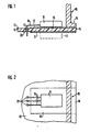
- FIG. 1 shows in FIG. 1 a partially shown control unit in longitudinal section and in FIG. 2 a plan view of a printed circuit board with cut represented housing.
- a layer 13 of good heat-conductive material is applied, which extends to the edge 14 of the circuit board.
- the layer 13 of good heat-conducting material is preferably metallic and may for example be a correspondingly formed conductor track, an umbrella surface for improving the electromagnetic compatibility (EMC), laminate, a copper cladding or the like.
- the power component 11 rests with its rear side 15 (largest surface) and is suitably bonded, for example glued, soldered, screwed.
- the resting rear side 15 of the power component 11 is smaller than the base area of the heat-conducting layer 13.
- the terminal electrodes 16 of the power device 11 initially run parallel to the printed circuit board 10, without touching the heat-conducting layer 13, and are bent outside thereof and guided into corresponding solder holes 17 of the circuit board. By soldering the power device is connected to the circuit.
- a hood-like cover 18 is placed, the peripheral edge 19 rests on the edge of the circuit board 10 on the same and thus also on the heat-conducting layer 13.
- the cover 18 or its edge 19 is suitably connected to the circuit board 10, for example, glued, screwed or soldered.
- the cover 18 is made of a heat-conducting material, preferably a metal, at least in the region of the heat-conducting layer 13, and serves as a cooling surface for the power component 11.
- the heat to be dissipated by the power component 11 is therefore conducted via the heat-conducting layer 13 to a cooling surface, the cover 17.
- a complex assembly of the power component on or on a special shape-matched cooling surface is eliminated.
- the cooling surface is therefore independent of the shape of the power device, that is, the shape of the power device affects neither the shape nor the location of the cooling surface.
- between the power device and the cooling surface need not exist a direct neighborhood situation.
- the bottom 20 can be equipped accordingly with power devices 11. These are then also on a heat-conducting layer 21, via which the heat to be dissipated is guided to a cooling surface, not shown.
- the surface of the heat-conducting layer can be structured accordingly.
- suitable measures for example, a solder layer or other heat-conducting layer can be embossed in a lattice structure, for example by a reflow soldering process.
- the respective metallic layers 13 should be insulated from one another, that is to say they do not touch one another.
- the cover of a housing or a - not shown - freely accessible cooling element e.g., cooling angle
- these are advantageously electrically insulated from the heat-conducting layer 13.
- either the cooling surface in the region of the contact point can be provided with an insulation layer, for example an anodized layer, a lacquer or the like.
- the corresponding cooling element can then also be used for cooling a plurality of power components.
- thermoelectric layer 13 It is also possible to provide the heat-conducting layer 13 with an insulating layer at least in the region of the cooling surface.
- an electrically conductive connection between the cooling surface and the heat-conducting layer 13 can also be useful for certain application stables, for example for improving the electromagnetic compatibility. These are then joined together without insulation
- a correspondingly broad conductor track or a shielding surface is used as the heat-conducting layer, it can be designed to improve the thermal conductivity correspondingly thicker (greater layer thickness).
- the layer thickness is increased to thicknesses above 50 ⁇ m, preferably to layer thicknesses of 100 ⁇ m to 200 ⁇ m.
- the printed circuit board 10 may be provided on both sides (page 12 or page 20) with heat-conducting layers which are interconnected via a known per se für Arichantechnik Thus, parallel heat dissipation paths are created.
- the surface of the heat-conducting layer 13 and the corresponding conductor track portion for a good assembly and contacting are preferably in a plane.
- the cover of a housing this may be formed so that at the same time an electromagnetic shielding of the covered circuit takes place (improvement of the electromagnetic compatibility, EMC).
- EMC electromagnetic compatibility
- This cover is then formed as a metallic or metallized box covering the corresponding PCB areas.
- This metallic box can then cover, for example, the entire board surface and rest on the edges of the circuit board. There is an electrical and thermally conductive contact. It is also possible to form this box so that it covers the circuit board only in the area in which sensitive components are arranged, ie, components that must be shielded with regard to the electromagnetic compatibility of the circuit. In this case, the power components to be cooled can be arranged inside or outside the box.
- connecting tabs can be attached to the underside of which protrude through corresponding openings of the circuit board or are passed past the edges.
- the box is placed on it after soldering the circuit board top, and the connecting tabs are bent or soldered.
- These connecting straps can also be used to fix a corresponding lower part (also an EMC box).
Landscapes
- Engineering & Computer Science (AREA)
- Microelectronics & Electronic Packaging (AREA)
- Physics & Mathematics (AREA)
- Thermal Sciences (AREA)
- Cooling Or The Like Of Electrical Apparatus (AREA)
- Shielding Devices Or Components To Electric Or Magnetic Fields (AREA)
- Structure Of Printed Boards (AREA)
- Mounting Of Printed Circuit Boards And The Like (AREA)
- Structures For Mounting Electric Components On Printed Circuit Boards (AREA)
Abstract
Description
- Die Erfindung geht aus von einem elektrischen Gerät nach der Gattung des Hauptanspruchs.
- Bei derartigen Geräten, wie sie beispielsweise aus der
EP 0 308 296 A1 bekannt sind, ist eine aus einer Kunststoffplatte bestehende Schaltungskarte bekannt, die auf beiden Seiten Kupferkaschierungen aufweist. Auf einer Seite werden elektronische Komponenten montiert, die andere Seite ist für die Lötverbindungen vorgesehen. Beide Seiten sind mit Leiterbahnen und mit Bauelementen versehen. Zwei wärmeleitende Bereiche sind auf der zur Montage der Bauelemente dienenden Seite und auf der für die Lötverbindungen dienenden Seite vorgesehen. Die Leiterbahnen und die wärmeleitenden Bereiche sind mit denselben Verfahrensschritten hergestellt. Ein Kühlelement ist auf der Leiterplatte befestigt, wobei die metallischen Bereiche mit einem oder mehreren Bauelementen thermisch gekoppelt werden. Die Schichtdicke der zur Wärmeableitung dienenden Bereiche ist größer als die Schichtdicke der zur elektrischen Kontaktierung dienenden Leiterbahnen. - Demgegenüber ist vorgesehen die Wärmeableitung zu verbessern.
- Das erfindungsgemäße elektrische Gesät mit den Merkmalen des Hauptanspruchs hat demgegenüber den Vorteil, daß, die wärmeleitende Schicht bis an den Rand der Leiterplatte reicht und daß das Kühlelement am Rand der Leiterplatte auf der wärmeleitenden Schicht aufliegt, wodurch die Wärmeabführung verbessert ist. Durch die gute Wärmeabführung ist auch eine höhere Umgebungstemperatur möglich, wie sie zum Beispiel im Motorraum eines Kraftfahrzeugs herrscht. Das Gehäuse des elektrischen Gerätes kann weiterhin mit einer geringen Anzahl von Fertigungsschritten automatisch bestückt und verlötet werden.
- Zwei Ausführungsbeispiele der Erfindung sind in der nachfolgenden Beschreibung und Zeichnung näher erläutert. Letztere zeigt in
Figur 1 ein nur teilweise dargestelltes Steuergerät im Längsschnitt und inFigur 2 eine Draufsicht auf eine Leiterplatte mit geschnitten dargestelltern Gehäuse. - In den
Figuren 1 und 2 ist mit 10 die Leiterplatte eines elektronischen Steuergerätes bezeichnet, die eine nicht näher dargestellte Schaltung trägt. Zu dieser Schaltung gehört auch ein sich in Betrieb stark erwärmendes Leistungsbauelement 11, dessen Wärme abzuleiten ist. - Auf die Oberseite 12 der Leiterplatte 10 ist eine Schicht 13 aus gut wärmeleiltendem Material aufgebracht, die bis an den Rand 14 der Leiterplatte reicht. Die Schicht 13 aus gut wärmeleitendem Material ist vorzugsweise metallisch und kann beispielsweise eine entsprechend ausgebildete Leiterbahn, eine Alschirmfläche zur Verbesserung der elektromagnetischen Verträglichkeit (EMV), Laminat, eine Kupferkaschierung oder ähnliches sein.
- Auf dieser wärmeleitenden Schicht 13 liegt das Leistungsbauelement 11 mit seiner Rückseite 15 (größte Fläche) auf und ist auf geeignete Weise betestigt, zum Beispiel verklebt, gelötet, geschraubt. Die aufliegende Rückseite 15 des Leistungsbauelementes 11 ist kleiner als die Grundfläche der wärmeleitenden Schicht 13.
- Die Anschlußelektroden 16 des Leistungsbauelementes 11 verlaufen zunächst parallel zur Leiterplatte 10, ohne die wärmeleitende Schicht 13 zu berühren, und sind außerhalb derselben abgebogen und in entsprechende Lötöffnungen 17 der Leiterplatte geführt. Durch Verlöten wird das Leistungsbauelement mit der Schaltung verbunden.
- Auf die Oberseite 12 der Leiterplatte 10 ist ein haubenartiger Deckel 18 aufgesetzt, dessen umlaufender Rand 19 am Rand der Leiterplatte 10 auf derselben und damit auch auf der wärmeleitenden Schicht 13 aufliegt. Der Deckel 18 bzw. dessen Rand 19 ist auf geeignete Weise mit der Leiterplatte 10 verbunden, zum Beispiel geklebt, geschraubt oder verlötet.
- Der Deckel 18 ist zumindest im Bereich der wärmeleitenden Schicht 13 aus einem wärmeleitenden Material vorzugsweise einem Metall, gefertigt und dient als Kühlfläche für das Leistungsbauelement 11.
- Die vom Leistungsbauelement 11 abzuleitende Wärme wird also über die wärmeleitende Schicht 13 zu einer Kühlfläche, dem Deckel 17, geleitet. Eine aufwendige Montage des Leistungsbauelementes auf oder an einer speziellen formangepaßten Kühlfläche entfällt. Die Kühlfläche ist demzufolge unabhängig von der Form des Leistungsbauelementes, das heißt die Form das Leistungsbauelementes beeinflußt weder die Form noch die Lage der Kühlfläche. Darüberhinaus braucht zwischen Leistungsbauelement und Kühlfläche keine direkte Nachbarschaftslage zu bestehen.
- Ist die Leiterplatte 10 - wie in
Figur 1 gestrichelt dargestellt - als Zweitagenleiterplatte ausgeführt, kann auch die Unterseite 20 entsprechend mit Leistungsbauelementen 11 bestückt werden. Diese liegen dann ebenfalls auf einer wärmeleitenden Schicht 21 auf, über die die abzuleitende Wärme an eine nicht dargestellte Kühlfläche geführt wird. - Zur Verbesserung des Wärmeübergangs zwischen der wärmeleitenden Schicht 13 bzw. 21 und der Kühlfläche kann die Oberfläche der wärmeleitenden Schicht entsprechend strukturiert werden. Durch geeignete Maßnahmen kann beispielsweise eine Lotschicht oder andere wärmeleitende Schicht in Gitterstruktur aufgeprägt werden, zum Beispiel durch ein Reflow-Lötverfahren.
- Zur weiteren Verbesserung des Wärmeübergangs ist eine großflächige Kontaktierung zwischen wärmeleitender Schicht 13 und Kühlfläche vorteilhaft.
- Sind mehrere Leistungsbauelemente 11 auf einer Seite 12 bzw. 20 der Leiterplatte nebeneinander angeordnet, sollten die jeweiligen metallischen Schichten 13 gegeneinander isoliert sein, das heißt einander nicht berühren.
- Ist die Kühlfläche wie im Ausführungsbeispiel dargestellt, der Deckel eines Gehäuses oder ein - nicht dargestelltes - frei zugängliches Kühlelement (z.B. Kühlwinkel), sind diese vorteilhafter Weise gegen die wärmeleitende Schicht 13 elektrisch isoliert. Dazu kann entweder die Kühlfläche im Bereich der Kontaktstelle mit einer Isolationsschicht versehen sein, zum Beispiel einer Eloxalschicht, einem Lack oder ähnlichem. Das entsprechende Kühlelement kann dann auch zur Kühlung mehrerer Leistungsbauelemente genutzt werden.
- Es ist auch möglich die wärmeleitende Schicht 13 zumindest im Bereich der Kühlfläche mit einer Isolationsschicht zu versehen.
- Im Gegensatz dazu kann aber auch bei bestimmten Anwendungställen, zum Beispiel zur Verbesserung der elektromagnetischen Verträglichkeit, eine elektrisch leitende Verbindung zwischen Kühlfläche und wärmeleitender Schicht 13 sinnvoll sein. Dazu werden diese dann ohne isolierung zusammengefügt
- Wird als wärmeleitende Schicht zum Beispiel eine entsprechend breit ausgebildete Leiterbahn oder eine Abschirmfläche genutzt, kann diese zur Verbesserung der Wärmeleitfähigkeit entsprechend dicker (größere Schichtdicke) ausgebildet sein.
- Im Verdrahtungsbereich der Leiterplatte wird dazu eine Lederschicht mit einer Stärke von z. B. 30 µm aufgetragen Damit können dann Leiterbahnen mit Breiten unter 200 µm und etwa gleich breiten Abständen zwischen den Leiterbahnen gefertigt werden.
- In den Bereichen, in denen elektrische Bauelemente wärmeleitend mit den Leiterbahnen verbunden werden sollen, wird die Schichtdicke erhöht auf Dicken über 50 µm, vorzugsweise auf Schichtdicken von 100 µm bis 200 µm.
- Zur weiteren Verbesserung der Wärmeleitfähigkeit kann die Leiterplatte 10 auf beiden Seiten (Seite 12 oder Seite 20) mit wärmeleitenden Schichten versehen sein, die über eine an sich bekannte Durchkontaktierung miteinander verbunden sind Damit werden parallele Wärmeableitwege geschaffen.
- Wird die Leiterplatte 10 im Bereich der wärmeleitenden Schicht mit SMD-Bauteilen (SMD = surface mounted device) bestückt, liegen die Oberfläche der wärmeleitenden Schicht 13 und die des entsprechenden Leiterbahnenabschnittes für eine gute Montage und Kontaktierung vorzugsweise in einer Ebene.
- Ist die Kühlfläche, wie im Ausführungsbeispiel dargestellt, der Deckel eines Gehäuses, kann dieser so ausgebildet sein, daß gleichzeitig eine elektromagnetische Schirmung der abgedeckten Schaltung erfolgt (Verbesserung der elektromagnetischen Verträglichkeit, EMV). Dieser Deckel wird dann als metallische bzw. metallisierte Box ausgebildet, die die entsprechenden Leiterplattenbereiche abdeckt. Diese metallische Box kann dann beispielsweise die gesamte Leiterplattenfläche abdecken und an den Rändern der Leiterplatte aufliegen. Dort erfolgt eine elektrische und wärmeleitende Kontaktierung. Es ist auch möglich, diese Box so auszubilden, daß sie die Leiterplatte nur in dem Bereich überdeckt, in dem empfindliche Bauelemente angeordnet sind, d. h. Bauelemente, die im Hinblick auf die elektromagnetische Verträglichkeit der Schaltung abgeschirmt werden müssen. Dabei können die zu kühlenden Leistungsbauelemente innerhalb oder außerhalb der Box angeordnet werden.
- Um diese Box mechanisch stabil und gut leitend mit der Leiterplatte zu verbinden, können an deren Unterseite Verbindungslaschen angebracht werden, die durch entsprechende Öffnungen der Leiterplatte ragen oder an deren Rändern vorbeigeführt werden. Die Box wird dazu nach dem Löten der Leiterplatten-Oberseite auf diese aufgesetzt, und die Verbindungslaschen werden umgebogen oder verlötet. Diese Verbindungslaschen können darüber hinaus zur Fixierung eines entsprechenden Unterteils (ebenfalls eine EMV-Box) genutzt werden.
Claims (12)
- Elektrisches Gerät, insbesondere Schalt- oder Steuergerät für Kraftfahrzeuge, mit einer eine elektronische Schaltung tragenden Leiterplatte (10), auf der Leiterbahnen zur elektrischen Kontaktierung und mindestens ein zu kühlendes Leistungsbauelement (11) angeordnet sind, wobei auf die Leiterplatte (10) zumindest im Bereich des Leistungsbauelements (11) eine wärmeleitende Schicht (13, 21) aufgebracht ist, auf der das Leistungsbauelement (11) aufliegt und wobei die wärmeleitende Schicht (13, 21) eine Leiterbahn ist, die die Wärme von dem Leistungsbauelement (11) direkt zu einem Kühlelement (18) ableitet, wobei die Schichtdicke der Leiterbahnen in den der Wärmeleitung dienenden Bereichen eine größere Dicke aufweist als in den der elektrischen Kontaktierung dienenden Bereichen, dadurch gekennzeichnet, daß die wärmeleitende Schicht (13) bis an den Rand (14) der Leiterplatte (10) reicht und daß das Kühlelement (18) am Rand (14) der Leiterplatte (10) auf der wärmeleitenden Schicht (13) aufliegt.
- Elektrisches Gerät nach Anspruch 1, dadurch gekennzeichnet, daß die wärmeleitende Schicht (13, 21) eine unterschiedliche Dicke aufweist.
- Elektrisches Gerät nach Anspruch 1, dadurch gekennzeichnet, daß die Schichtdicke im Bereich der wärmeleitenden Schicht (13) größer als 70 µm ist, und daß die Schichtdicke der Leiterbahnen in den im wesentlichen nicht wärmeleitenden Bereichen etwa 30 µm beträgt.
- Elektrisches Gerät nach einem der Ansprüche 1 bis 3, dadurch gekennzeichnet, daß das Leistungsbauelement (111) mit einer seiner Flächen, vorzugsweise der größten Fläche (15) flächig auf der wärmeleitenden Schicht (13, 21) aufliegt.
- Elektrisches Gerät nach einem der Ansprüche 1 bis 4, dadurch gekennzeichnet, daß das Kühlelement (18, 19) Teil eines die Leiterplatte (10) aufnehmenden Gehäuses ist.
- Elektrisches Gerät nach einem der Ansprüche 1 bis 5, dadurch gekennzeichnet, daß das Kühlelement ein freistehender metallischer Körper ist.
- Elektrisches Gerät nach einem der Ansprüche 1 bis 6, dadurch gekennzeichnet, daß die wärmeleitende Schicht (13, 21) und die Kühlfläche (18, 19) elektrisch gegeneinander isoliert sind.
- Elektrisches Gerät nach einem der Ansprüche 1 bis 7, dadurch gekennzeichnet, daß auf die Leiterplatte (10) beidseitig wärmeleitende Schichten (13, 21) aufgebracht sind.
- Elektrisches Gerät nach Anspruch 8, dadurch gekennzeichnet, daß die wärmeleitenden Schichten (13, 21) über Durchkontektierungen verbunden sind.
- Elektrisches Gerät nach einem der Ansprüche 1 bis 9, dadurch gekennzeiehnet, daß das Kühlelement Teil eines elektromagnetisch abschirmenden Gehäusebauteils ist.
- Elektrisches Gerät nach Anspruch 10, dadurch gekennzeichnet, daß die zu kühlenden Leistungsbauelemente (11) innerhalb des elektromagnetisch abschirmenden Gehäusebauteils angeordnet ist.
- Elektrisches Gerät nach Anspruch 5, dadurch gekennzeichnet, daß die zu kühlenden Leistungsbauelemente (11) außerhalb des elektromagnetisch beschirmenden Gehäusebauteils angeordnet sind.
Applications Claiming Priority (5)
| Application Number | Priority Date | Filing Date | Title |
|---|---|---|---|
| DE4131515 | 1991-09-21 | ||
| DE4131515 | 1991-09-21 | ||
| DE4222838A DE4222838C2 (de) | 1991-09-21 | 1992-07-11 | Elektrisches Gerät, insbesondere Schalt- und Steuergerät für Kraftfahrzeuge |
| DE4222838 | 1992-07-11 | ||
| PCT/DE1992/000721 WO1993006705A1 (de) | 1991-09-21 | 1992-09-09 | Elektrisches gerät, insbesondere schalt- und steuergerät für kraftfahrzeuge |
Publications (3)
| Publication Number | Publication Date |
|---|---|
| EP0558712A1 EP0558712A1 (de) | 1993-09-08 |
| EP0558712B1 EP0558712B1 (de) | 1996-12-11 |
| EP0558712B2 true EP0558712B2 (de) | 2010-04-07 |
Family
ID=25907572
Family Applications (1)
| Application Number | Title | Priority Date | Filing Date |
|---|---|---|---|
| EP92918773A Expired - Lifetime EP0558712B2 (de) | 1991-09-21 | 1992-09-09 | Elektrisches gerät, insbesondere schalt- und steuergerät für kraftfahrzeuge |
Country Status (5)
| Country | Link |
|---|---|
| US (1) | US6222732B1 (de) |
| EP (1) | EP0558712B2 (de) |
| JP (1) | JPH06503210A (de) |
| ES (1) | ES2095486T5 (de) |
| WO (1) | WO1993006705A1 (de) |
Families Citing this family (34)
| Publication number | Priority date | Publication date | Assignee | Title |
|---|---|---|---|---|
| DE4432057A1 (de) * | 1994-09-09 | 1996-03-14 | Bosch Gmbh Robert | Vorrichtung zur Ableitung der thermischen Verlustleistung eines elektronischen oder elektromechanischen Bauelementes |
| JP2000082774A (ja) * | 1998-06-30 | 2000-03-21 | Sumitomo Electric Ind Ltd | パワ―モジュ―ル用基板およびその基板を用いたパワ―モジュ―ル |
| US6320723B1 (en) * | 1999-06-24 | 2001-11-20 | Seagate Technology Llc | Protective cover for a disc drive printed circuit board wherein the cover and a circuit board component are thermally connected |
| ES2160505B1 (es) * | 1999-08-09 | 2003-04-01 | Mecanismos Aux Es Ind S L | Caja de interconexiones de automovil con disipacion termica mejorada. |
| JP4142227B2 (ja) * | 2000-01-28 | 2008-09-03 | サンデン株式会社 | 車両用電動圧縮機のモータ駆動用インバータ装置 |
| JP3923703B2 (ja) * | 2000-03-29 | 2007-06-06 | ローム株式会社 | 放熱手段を有するプリント配線板 |
| US6377462B1 (en) * | 2001-01-09 | 2002-04-23 | Deere & Company | Circuit board assembly with heat sinking |
| DE10150581A1 (de) * | 2001-10-12 | 2003-04-17 | Schlafhorst & Co W | Garnsensor |
| DE10152475A1 (de) * | 2001-10-24 | 2003-05-08 | Hella Kg Hueck & Co | Wärmeleitendes Verbindungsstück |
| DE10162600A1 (de) * | 2001-12-20 | 2003-07-10 | Bosch Gmbh Robert | Gehäuseanordnung für ein elektrisches Gerät |
| US6587346B1 (en) * | 2002-01-31 | 2003-07-01 | Visteon Global Technologies, Inc. | Combination electrical power distribution and heat dissipating device |
| US6583988B1 (en) * | 2002-02-05 | 2003-06-24 | Whelen Engineering Company, Inc. | Encapsulated power supply |
| WO2003094586A1 (de) * | 2002-04-29 | 2003-11-13 | Siemens Aktiengesellschaft | Leiterplatte mit smd-bauelement und kühlkörper |
| US6797889B1 (en) * | 2002-05-30 | 2004-09-28 | Johnson Controls Automotive Electronics | Assembly of power circuits and numerical data printed on a multilayer board |
| US7190589B2 (en) * | 2004-10-19 | 2007-03-13 | Cinch Connectors, Inc. | Electronic control enclosure |
| CN1993032A (zh) * | 2005-12-27 | 2007-07-04 | 华硕电脑股份有限公司 | 具有高电磁兼容性之电子装置 |
| JP2007324200A (ja) * | 2006-05-30 | 2007-12-13 | Yazaki Corp | 回路基板およびそれを備えた電気接続箱 |
| US7561430B2 (en) * | 2007-04-30 | 2009-07-14 | Watlow Electric Manufacturing Company | Heat management system for a power switching device |
| DE102007025957A1 (de) * | 2007-06-04 | 2008-12-11 | Robert Bosch Gmbh | Verfahren und Vorrichtung zum Festlegen eines eine elektrische Schaltung oder dergleichen aufweisenden Flächensubstrats in einer Einbauposition |
| US20090091889A1 (en) * | 2007-10-09 | 2009-04-09 | Oman Todd P | Power electronic module having improved heat dissipation capability |
| DE102008026627B3 (de) * | 2008-06-03 | 2009-10-29 | Siemens Aktiengesellschaft | Kühlsystem für LED-Chip-Anordnung |
| KR20100007470A (ko) * | 2008-07-14 | 2010-01-22 | 엘지전자 주식회사 | 플라즈마 디스플레이 장치 |
| US8804337B2 (en) * | 2012-03-26 | 2014-08-12 | Hamilton Sundstrand Space Systems International, Inc. | Structural assembly for cold plate cooling |
| DE102013107977B4 (de) * | 2013-04-29 | 2021-01-07 | Avl Software And Functions Gmbh | Vorrichtung zum Verbinden eines Gerätes mit einer integrierten Elektronikbaugruppe |
| US10019046B2 (en) * | 2015-08-17 | 2018-07-10 | Asia Vital Components Co., Ltd. | Internal frame structure with heat insulation effect and electronic apparatus with the internal frame structure |
| DE102017212968B4 (de) * | 2016-08-05 | 2024-02-01 | Robert Bosch Gmbh | Gehäuseaufbau für eine elektronische steuereinheit und herstellungsverfahren |
| CN108990251B (zh) * | 2017-06-02 | 2020-12-25 | 台达电子工业股份有限公司 | 印刷电路板组装结构及其组装方法 |
| DE102017214267B4 (de) * | 2017-08-16 | 2025-02-20 | Mahle International Gmbh | Kühlvorrichtung und Verfahren zum Herstellen der Kühlvorrichtung |
| JP6852649B2 (ja) * | 2017-10-24 | 2021-03-31 | 株式会社オートネットワーク技術研究所 | 回路構成体及び回路構成体の製造方法 |
| DE102018217607A1 (de) | 2018-10-15 | 2020-04-16 | Continental Automotive Gmbh | Halbleiterbauelement-Anordnung, Verfahren zu deren Herstellung sowie Entwärmungseinrichtung |
| DE102019215523A1 (de) | 2019-10-10 | 2021-04-15 | Vitesco Technologies GmbH | Leistungshalbleiterbauteil sowie Verfahren zur Herstellung eines Leistungshalbleiterbauteils |
| EP3876688B1 (de) * | 2020-03-03 | 2024-01-31 | Honeywell International Inc. | Stützer für leiterplatte mit temperaturveränderlichem elektrischem element |
| CN113490368B (zh) | 2021-07-07 | 2023-03-21 | 台达电子企业管理(上海)有限公司 | 电源装置及大功率照明系统 |
| CN116321991A (zh) * | 2023-04-24 | 2023-06-23 | 台达电子企业管理(上海)有限公司 | 功率元件组装结构 |
Citations (8)
| Publication number | Priority date | Publication date | Assignee | Title |
|---|---|---|---|---|
| US3631325A (en) † | 1970-06-15 | 1971-12-28 | Sperry Rand Corp | Card module and end wall treatment facilitating heat transfer and sliding |
| DE2226395A1 (de) † | 1972-05-31 | 1973-12-13 | Bosch Gmbh Robert | Elektrische schaltungsanordnung |
| DE8114325U1 (de) † | 1981-05-14 | 1982-09-30 | Siemens AG, 1000 Berlin und 8000 München | Wärmeableitungsvorrichtung |
| DE3115017A1 (de) † | 1981-04-14 | 1982-11-04 | Blaupunkt-Werke Gmbh, 3200 Hildesheim | Elektronisches bauelement |
| DE3305167A1 (de) † | 1983-02-15 | 1984-08-16 | Robert Bosch Gmbh, 7000 Stuttgart | Elektrische schaltungsanordnung mit einer leiterplatte |
| DE3437774A1 (de) † | 1984-10-16 | 1986-04-17 | Telefonbau & Normalzeit Gmbh | Anordnung zur kuehlung von auf senkrecht stehenden einreihigen schaltungsmodulen aufgebrachten leistungshalbleitern |
| EP0308296A1 (de) † | 1987-09-16 | 1989-03-22 | Telemecanique | Mit einer Wärmeabfuhrvorrichtung versehene gedruckte Schaltung |
| DE3832856A1 (de) † | 1988-09-28 | 1990-03-29 | Standard Elektrik Lorenz Ag | Leiterplatte mit einem waermeleitenden element |
Family Cites Families (14)
| Publication number | Priority date | Publication date | Assignee | Title |
|---|---|---|---|---|
| US3061760A (en) * | 1959-12-10 | 1962-10-30 | Philco Corp | Electrical apparatus |
| US3919602A (en) | 1972-03-23 | 1975-11-11 | Bosch Gmbh Robert | Electric circuit arrangement and method of making the same |
| DE2214163A1 (de) | 1972-03-23 | 1973-10-11 | Bosch Gmbh Robert | Elektrische schaltungsanordnung |
| US3885304A (en) | 1972-03-23 | 1975-05-27 | Bosch Gmbh Robert | Electric circuit arrangement and method of making the same |
| IT1008331B (it) | 1973-03-28 | 1976-11-10 | Rca Corp | Pannello composito a circuito stampato |
| US4204247A (en) * | 1978-09-22 | 1980-05-20 | Cps, Inc. | Heat dissipating circuit board assembly |
| US4339260A (en) | 1981-01-12 | 1982-07-13 | Owens-Illinois, Inc. | Environmentally protected electronic control for a glassware forming machine |
| DE3210019C2 (de) | 1982-03-19 | 1984-04-19 | Ford-Werke AG, 5000 Köln | Gehäuse für eine Heizungs- oder Klimaanlage für Kraftfahrzeuge |
| US4475145A (en) * | 1982-07-12 | 1984-10-02 | Rockwell International Corporation | Circuit board heatsink assembly and technique |
| WO1987004892A1 (fr) * | 1986-02-06 | 1987-08-13 | Fujitsu Limited | Structure de mise a la terre d'une carte de circuits imprimes a noyau metallique |
| US4811165A (en) * | 1987-12-07 | 1989-03-07 | Motorola, Inc. | Assembly for circuit modules |
| US4941067A (en) * | 1989-04-07 | 1990-07-10 | Motorola Inc. | Thermal shunt for electronic circuits |
| US5019941A (en) * | 1989-11-03 | 1991-05-28 | Motorola, Inc. | Electronic assembly having enhanced heat dissipating capabilities |
| JPH04121793U (ja) * | 1991-04-17 | 1992-10-30 | パイオニア株式会社 | ヒートシンク・基板アセンブリ |
-
1992
- 1992-09-09 US US08/064,010 patent/US6222732B1/en not_active Expired - Lifetime
- 1992-09-09 WO PCT/DE1992/000721 patent/WO1993006705A1/de not_active Ceased
- 1992-09-09 EP EP92918773A patent/EP0558712B2/de not_active Expired - Lifetime
- 1992-09-09 ES ES92918773T patent/ES2095486T5/es not_active Expired - Lifetime
- 1992-09-09 JP JP5505680A patent/JPH06503210A/ja active Pending
Patent Citations (8)
| Publication number | Priority date | Publication date | Assignee | Title |
|---|---|---|---|---|
| US3631325A (en) † | 1970-06-15 | 1971-12-28 | Sperry Rand Corp | Card module and end wall treatment facilitating heat transfer and sliding |
| DE2226395A1 (de) † | 1972-05-31 | 1973-12-13 | Bosch Gmbh Robert | Elektrische schaltungsanordnung |
| DE3115017A1 (de) † | 1981-04-14 | 1982-11-04 | Blaupunkt-Werke Gmbh, 3200 Hildesheim | Elektronisches bauelement |
| DE8114325U1 (de) † | 1981-05-14 | 1982-09-30 | Siemens AG, 1000 Berlin und 8000 München | Wärmeableitungsvorrichtung |
| DE3305167A1 (de) † | 1983-02-15 | 1984-08-16 | Robert Bosch Gmbh, 7000 Stuttgart | Elektrische schaltungsanordnung mit einer leiterplatte |
| DE3437774A1 (de) † | 1984-10-16 | 1986-04-17 | Telefonbau & Normalzeit Gmbh | Anordnung zur kuehlung von auf senkrecht stehenden einreihigen schaltungsmodulen aufgebrachten leistungshalbleitern |
| EP0308296A1 (de) † | 1987-09-16 | 1989-03-22 | Telemecanique | Mit einer Wärmeabfuhrvorrichtung versehene gedruckte Schaltung |
| DE3832856A1 (de) † | 1988-09-28 | 1990-03-29 | Standard Elektrik Lorenz Ag | Leiterplatte mit einem waermeleitenden element |
Also Published As
| Publication number | Publication date |
|---|---|
| WO1993006705A1 (de) | 1993-04-01 |
| JPH06503210A (ja) | 1994-04-07 |
| ES2095486T5 (es) | 2010-07-09 |
| EP0558712A1 (de) | 1993-09-08 |
| ES2095486T3 (es) | 1997-02-16 |
| US6222732B1 (en) | 2001-04-24 |
| EP0558712B1 (de) | 1996-12-11 |
Similar Documents
| Publication | Publication Date | Title |
|---|---|---|
| EP0558712B2 (de) | Elektrisches gerät, insbesondere schalt- und steuergerät für kraftfahrzeuge | |
| DE10056832B4 (de) | Halbleiterbauteil-Moduleinheit | |
| EP1648744B1 (de) | Elektronikeinheit sowie verfahren zur herstellung einer elektronikeinheit | |
| DE19854180B4 (de) | Modulgehäuse für Halbleiterbauteile | |
| EP0588793B1 (de) | Gehäuse für kfz-elektronik | |
| DE4222838C2 (de) | Elektrisches Gerät, insbesondere Schalt- und Steuergerät für Kraftfahrzeuge | |
| EP0876743B1 (de) | Steuergerät, insbesondere für ein kraftfahrzeug | |
| EP1459611B1 (de) | Gehäuseanordnung für ein elektrisches gerät | |
| DE4017697C2 (de) | Elektronisches Bauelement, Verfahren zu dessen Herstellung und Verwendung | |
| EP0920055B1 (de) | Kühlvorrichtung für ein auf einer Leiterplatte angeordnetes, wärmeerzeugendes Bauelement | |
| DE4218112B4 (de) | Elektrisches Gerät, insbesondere Schalt- und Steuergerät für Kraftfahrzeuge | |
| EP1450404B1 (de) | Anordnung in Druckkontaktierung mit einem Leistungshalbleitermodul | |
| DE69507370T2 (de) | Leiterplattenanordnung | |
| EP0855090B1 (de) | Multichipmodul | |
| EP0368142B1 (de) | Elektronisches Steuergerät | |
| WO2009043649A2 (de) | Dreidimensionaler elektronischer schaltungsträgeraufbau, sowie schaltungsgrundträger aufweisend den schaltungsträgeraufbau als funktionsbauteil und dreidimensionale schaltungsanordnung bestehend aus zumindest zwei derartigen dreidimensionalen schaltungsträgeraufbauten | |
| EP1445799B1 (de) | Kühleinrichtung für Halbleiter auf Leiterplatte | |
| DE4332115B4 (de) | Anordnung zur Kühlung mindestens einen Kühlkörper aufweisenden Leiterplatte | |
| DE4335946C2 (de) | Anordnung bestehend aus einer Leiterplatte | |
| DE19859739A1 (de) | Kühlvorrichtung, insbesondere zur Verwendung in einem elektronischen Steuergerät | |
| DE102005049872B4 (de) | IC-Bauelement mit Kühlanordnung | |
| DE19518522A1 (de) | Steuergerät für ein Kraftfahrzeug | |
| DE3305167C2 (de) | Elektrische Schaltungsanordnung mit einer Leiterplatte | |
| DE102006008807B4 (de) | Anordnung mit einem Leistungshalbleitermodul und einem Kühlbauteil | |
| EP0489958B1 (de) | Leiterplatte für elektronische Steuergeräte und Verfahren zum Herstellen einer solchen Leiterplatte |
Legal Events
| Date | Code | Title | Description |
|---|---|---|---|
| PUAI | Public reference made under article 153(3) epc to a published international application that has entered the european phase |
Free format text: ORIGINAL CODE: 0009012 |
|
| 17P | Request for examination filed |
Effective date: 19930428 |
|
| AK | Designated contracting states |
Kind code of ref document: A1 Designated state(s): DE ES FR GB IT |
|
| 17Q | First examination report despatched |
Effective date: 19940502 |
|
| GRAG | Despatch of communication of intention to grant |
Free format text: ORIGINAL CODE: EPIDOS AGRA |
|
| GRAH | Despatch of communication of intention to grant a patent |
Free format text: ORIGINAL CODE: EPIDOS IGRA |
|
| GRAH | Despatch of communication of intention to grant a patent |
Free format text: ORIGINAL CODE: EPIDOS IGRA |
|
| GRAA | (expected) grant |
Free format text: ORIGINAL CODE: 0009210 |
|
| AK | Designated contracting states |
Kind code of ref document: B1 Designated state(s): DE ES FR GB IT |
|
| ET | Fr: translation filed | ||
| GBT | Gb: translation of ep patent filed (gb section 77(6)(a)/1977) |
Effective date: 19961211 |
|
| REF | Corresponds to: |
Ref document number: 59207677 Country of ref document: DE Date of ref document: 19970123 |
|
| REG | Reference to a national code |
Ref country code: ES Ref legal event code: FG2A Ref document number: 2095486 Country of ref document: ES Kind code of ref document: T3 |
|
| ITF | It: translation for a ep patent filed | ||
| PLBQ | Unpublished change to opponent data |
Free format text: ORIGINAL CODE: EPIDOS OPPO |
|
| PLBI | Opposition filed |
Free format text: ORIGINAL CODE: 0009260 |
|
| PLBI | Opposition filed |
Free format text: ORIGINAL CODE: 0009260 |
|
| 26 | Opposition filed |
Opponent name: EBM WERKE GMBH & CO. Effective date: 19970823 Opponent name: LEOPOLD KOSTAL GMBH & CO. KG Effective date: 19970821 |
|
| PLBF | Reply of patent proprietor to notice(s) of opposition |
Free format text: ORIGINAL CODE: EPIDOS OBSO |
|
| 26 | Opposition filed |
Opponent name: MANNESMANN VDO AG Effective date: 19970911 Opponent name: EBM WERKE GMBH & CO. Effective date: 19970823 Opponent name: LEOPOLD KOSTAL GMBH & CO. KG Effective date: 19970821 |
|
| PLBF | Reply of patent proprietor to notice(s) of opposition |
Free format text: ORIGINAL CODE: EPIDOS OBSO |
|
| PLBF | Reply of patent proprietor to notice(s) of opposition |
Free format text: ORIGINAL CODE: EPIDOS OBSO |
|
| RDAH | Patent revoked |
Free format text: ORIGINAL CODE: EPIDOS REVO |
|
| APAC | Appeal dossier modified |
Free format text: ORIGINAL CODE: EPIDOS NOAPO |
|
| APAE | Appeal reference modified |
Free format text: ORIGINAL CODE: EPIDOS REFNO |
|
| PLBQ | Unpublished change to opponent data |
Free format text: ORIGINAL CODE: EPIDOS OPPO |
|
| PLAB | Opposition data, opponent's data or that of the opponent's representative modified |
Free format text: ORIGINAL CODE: 0009299OPPO |
|
| APAC | Appeal dossier modified |
Free format text: ORIGINAL CODE: EPIDOS NOAPO |
|
| R26 | Opposition filed (corrected) |
Opponent name: LEOPOLD KOSTAL GMBH & CO. KG * 19970823 EBM WERKE Effective date: 19970821 |
|
| REG | Reference to a national code |
Ref country code: GB Ref legal event code: IF02 |
|
| PLBQ | Unpublished change to opponent data |
Free format text: ORIGINAL CODE: EPIDOS OPPO |
|
| PLAB | Opposition data, opponent's data or that of the opponent's representative modified |
Free format text: ORIGINAL CODE: 0009299OPPO |
|
| APAC | Appeal dossier modified |
Free format text: ORIGINAL CODE: EPIDOS NOAPO |
|
| R26 | Opposition filed (corrected) |
Opponent name: LEOPOLD KOSTAL GMBH & CO. KG * 19970823 EBM WERKE Effective date: 19970821 |
|
| PLAY | Examination report in opposition despatched + time limit |
Free format text: ORIGINAL CODE: EPIDOSNORE2 |
|
| PLAY | Examination report in opposition despatched + time limit |
Free format text: ORIGINAL CODE: EPIDOSNORE2 |
|
| PLAB | Opposition data, opponent's data or that of the opponent's representative modified |
Free format text: ORIGINAL CODE: 0009299OPPO |
|
| R26 | Opposition filed (corrected) |
Opponent name: MANNESMANN VDO AG Effective date: 19970911 Opponent name: EBM-PAPST MULFINGEN GMBH & CO. KGDR. SOLF Effective date: 19970823 Opponent name: LEOPOLD KOSTAL GMBH & CO. KG Effective date: 19970821 |
|
| PLBC | Reply to examination report in opposition received |
Free format text: ORIGINAL CODE: EPIDOSNORE3 |
|
| APAH | Appeal reference modified |
Free format text: ORIGINAL CODE: EPIDOSCREFNO |
|
| PLAB | Opposition data, opponent's data or that of the opponent's representative modified |
Free format text: ORIGINAL CODE: 0009299OPPO |
|
| PUAH | Patent maintained in amended form |
Free format text: ORIGINAL CODE: 0009272 |
|
| 27A | Patent maintained in amended form |
Effective date: 20100407 |
|
| AK | Designated contracting states |
Kind code of ref document: B2 Designated state(s): DE ES FR GB IT |
|
| REG | Reference to a national code |
Ref country code: ES Ref legal event code: DC2A Date of ref document: 20100610 Kind code of ref document: T5 |
|
| PGFP | Annual fee paid to national office [announced via postgrant information from national office to epo] |
Ref country code: IT Payment date: 20100925 Year of fee payment: 19 |
|
| PGFP | Annual fee paid to national office [announced via postgrant information from national office to epo] |
Ref country code: DE Payment date: 20101126 Year of fee payment: 19 |
|
| PGFP | Annual fee paid to national office [announced via postgrant information from national office to epo] |
Ref country code: ES Payment date: 20110923 Year of fee payment: 20 Ref country code: FR Payment date: 20111005 Year of fee payment: 20 Ref country code: GB Payment date: 20110923 Year of fee payment: 20 |
|
| REG | Reference to a national code |
Ref country code: DE Ref legal event code: R071 Ref document number: 59207677 Country of ref document: DE |
|
| REG | Reference to a national code |
Ref country code: DE Ref legal event code: R071 Ref document number: 59207677 Country of ref document: DE |
|
| REG | Reference to a national code |
Ref country code: GB Ref legal event code: PE20 Expiry date: 20120908 |
|
| PG25 | Lapsed in a contracting state [announced via postgrant information from national office to epo] |
Ref country code: DE Free format text: LAPSE BECAUSE OF EXPIRATION OF PROTECTION Effective date: 20120911 Ref country code: GB Free format text: LAPSE BECAUSE OF EXPIRATION OF PROTECTION Effective date: 20120908 |
|
| REG | Reference to a national code |
Ref country code: ES Ref legal event code: FD2A Effective date: 20130717 |
|
| PG25 | Lapsed in a contracting state [announced via postgrant information from national office to epo] |
Ref country code: ES Free format text: LAPSE BECAUSE OF EXPIRATION OF PROTECTION Effective date: 20120910 |