EP0556581B1 - Verfahren zur Herstellung eines oxidkeramischen Supraleiters mit hoher Kerndichte - Google Patents
Verfahren zur Herstellung eines oxidkeramischen Supraleiters mit hoher Kerndichte Download PDFInfo
- Publication number
- EP0556581B1 EP0556581B1 EP93100838A EP93100838A EP0556581B1 EP 0556581 B1 EP0556581 B1 EP 0556581B1 EP 93100838 A EP93100838 A EP 93100838A EP 93100838 A EP93100838 A EP 93100838A EP 0556581 B1 EP0556581 B1 EP 0556581B1
- Authority
- EP
- European Patent Office
- Prior art keywords
- superconducting
- density
- shaping
- composite body
- core
- Prior art date
- Legal status (The legal status is an assumption and is not a legal conclusion. Google has not performed a legal analysis and makes no representation as to the accuracy of the status listed.)
- Expired - Lifetime
Links
- 239000002887 superconductor Substances 0.000 title claims description 18
- 238000004519 manufacturing process Methods 0.000 title description 8
- 239000000919 ceramic Substances 0.000 title description 2
- 239000000463 material Substances 0.000 claims description 20
- 239000002131 composite material Substances 0.000 claims description 19
- 229910052574 oxide ceramic Inorganic materials 0.000 claims description 10
- 239000011224 oxide ceramic Substances 0.000 claims description 8
- 238000007493 shaping process Methods 0.000 claims description 7
- 238000000034 method Methods 0.000 claims description 6
- 239000004020 conductor Substances 0.000 claims description 5
- QVGXLLKOCUKJST-UHFFFAOYSA-N atomic oxygen Chemical compound [O] QVGXLLKOCUKJST-UHFFFAOYSA-N 0.000 claims description 4
- 239000001301 oxygen Substances 0.000 claims description 4
- 229910052760 oxygen Inorganic materials 0.000 claims description 4
- 238000005096 rolling process Methods 0.000 claims description 3
- 238000011084 recovery Methods 0.000 claims description 2
- 238000002844 melting Methods 0.000 description 7
- 230000008018 melting Effects 0.000 description 7
- 239000000843 powder Substances 0.000 description 6
- 238000010438 heat treatment Methods 0.000 description 5
- 238000005098 hot rolling Methods 0.000 description 5
- 238000001125 extrusion Methods 0.000 description 4
- BQCADISMDOOEFD-UHFFFAOYSA-N Silver Chemical compound [Ag] BQCADISMDOOEFD-UHFFFAOYSA-N 0.000 description 3
- 239000000155 melt Substances 0.000 description 3
- 239000011148 porous material Substances 0.000 description 3
- 239000011257 shell material Substances 0.000 description 3
- 229910052709 silver Inorganic materials 0.000 description 3
- 239000004332 silver Substances 0.000 description 3
- 229910001316 Ag alloy Inorganic materials 0.000 description 2
- IJGRMHOSHXDMSA-UHFFFAOYSA-N Atomic nitrogen Chemical compound N#N IJGRMHOSHXDMSA-UHFFFAOYSA-N 0.000 description 2
- 230000000052 comparative effect Effects 0.000 description 2
- 239000007788 liquid Substances 0.000 description 2
- 239000008188 pellet Substances 0.000 description 2
- OKTJSMMVPCPJKN-UHFFFAOYSA-N Carbon Chemical compound [C] OKTJSMMVPCPJKN-UHFFFAOYSA-N 0.000 description 1
- 238000000137 annealing Methods 0.000 description 1
- 239000012300 argon atmosphere Substances 0.000 description 1
- 230000015572 biosynthetic process Effects 0.000 description 1
- 238000005253 cladding Methods 0.000 description 1
- 238000005516 engineering process Methods 0.000 description 1
- 238000002474 experimental method Methods 0.000 description 1
- 229910002804 graphite Inorganic materials 0.000 description 1
- 239000010439 graphite Substances 0.000 description 1
- 238000001513 hot isostatic pressing Methods 0.000 description 1
- 238000007731 hot pressing Methods 0.000 description 1
- 230000002706 hydrostatic effect Effects 0.000 description 1
- 238000005461 lubrication Methods 0.000 description 1
- 229910052751 metal Inorganic materials 0.000 description 1
- 239000002184 metal Substances 0.000 description 1
- 229910052757 nitrogen Inorganic materials 0.000 description 1
- 239000000725 suspension Substances 0.000 description 1
- 238000003826 uniaxial pressing Methods 0.000 description 1
Images
Classifications
-
- H—ELECTRICITY
- H10—SEMICONDUCTOR DEVICES; ELECTRIC SOLID-STATE DEVICES NOT OTHERWISE PROVIDED FOR
- H10N—ELECTRIC SOLID-STATE DEVICES NOT OTHERWISE PROVIDED FOR
- H10N60/00—Superconducting devices
- H10N60/01—Manufacture or treatment
- H10N60/0268—Manufacture or treatment of devices comprising copper oxide
- H10N60/0801—Manufacture or treatment of filaments or composite wires
-
- Y—GENERAL TAGGING OF NEW TECHNOLOGICAL DEVELOPMENTS; GENERAL TAGGING OF CROSS-SECTIONAL TECHNOLOGIES SPANNING OVER SEVERAL SECTIONS OF THE IPC; TECHNICAL SUBJECTS COVERED BY FORMER USPC CROSS-REFERENCE ART COLLECTIONS [XRACs] AND DIGESTS
- Y10—TECHNICAL SUBJECTS COVERED BY FORMER USPC
- Y10S—TECHNICAL SUBJECTS COVERED BY FORMER USPC CROSS-REFERENCE ART COLLECTIONS [XRACs] AND DIGESTS
- Y10S505/00—Superconductor technology: apparatus, material, process
- Y10S505/70—High TC, above 30 k, superconducting device, article, or structured stock
- Y10S505/704—Wire, fiber, or cable
-
- Y—GENERAL TAGGING OF NEW TECHNOLOGICAL DEVELOPMENTS; GENERAL TAGGING OF CROSS-SECTIONAL TECHNOLOGIES SPANNING OVER SEVERAL SECTIONS OF THE IPC; TECHNICAL SUBJECTS COVERED BY FORMER USPC CROSS-REFERENCE ART COLLECTIONS [XRACs] AND DIGESTS
- Y10—TECHNICAL SUBJECTS COVERED BY FORMER USPC
- Y10S—TECHNICAL SUBJECTS COVERED BY FORMER USPC CROSS-REFERENCE ART COLLECTIONS [XRACs] AND DIGESTS
- Y10S505/00—Superconductor technology: apparatus, material, process
- Y10S505/725—Process of making or treating high tc, above 30 k, superconducting shaped material, article, or device
- Y10S505/739—Molding, coating, shaping, or casting of superconducting material
-
- Y—GENERAL TAGGING OF NEW TECHNOLOGICAL DEVELOPMENTS; GENERAL TAGGING OF CROSS-SECTIONAL TECHNOLOGIES SPANNING OVER SEVERAL SECTIONS OF THE IPC; TECHNICAL SUBJECTS COVERED BY FORMER USPC CROSS-REFERENCE ART COLLECTIONS [XRACs] AND DIGESTS
- Y10—TECHNICAL SUBJECTS COVERED BY FORMER USPC
- Y10S—TECHNICAL SUBJECTS COVERED BY FORMER USPC CROSS-REFERENCE ART COLLECTIONS [XRACs] AND DIGESTS
- Y10S505/00—Superconductor technology: apparatus, material, process
- Y10S505/725—Process of making or treating high tc, above 30 k, superconducting shaped material, article, or device
- Y10S505/739—Molding, coating, shaping, or casting of superconducting material
- Y10S505/74—To form wire or fiber
Definitions
- the invention relates to a method for producing a superconducting composite body by introducing an oxide-ceramic superconducting material into a shell, cross-section-reducing deformation and heat treatment for recovery and adjustment of the oxygen concentration, and a corresponding superconducting composite body.
- HTSL oxide-ceramic high-temperature superconductors
- oxide-ceramic powder is poured into a metal tube, for example, and a wire or a strip is produced by reducing the cross-section. Finally, a heat treatment is carried out, which is used to generate the continuous superconducting connection through the HTSL material and to optimize the critical current density.
- the shell usually consists of silver or silver alloys, since these materials ensure oxygen permeation through the shell material during the final heat treatment in order to set the optimum oxygen content.
- powder or a melt pressed into bars or pellets can also be filled into the cladding tubes.
- a filling density of approx. 55%, based on the theoretical HTSL density is achieved.
- the powders are pressed into bars or pellets, filling densities of about 70% are achieved and when filling a melt, a filling density of up to 100% is achieved.
- the core density of the oxide-ceramic superconductor material is typically 65 to 75% of the theoretical density. In the final annealing to set the superconducting properties, large pores are formed in the HTSL core due to the partial melting of the core, which results in a greatly reduced critical current density. These pores are therefore undesirable and should largely be avoided.
- the object of the invention is therefore to provide, in the case of a superconductor wire in which the superconductor material is in a sheath, a method for producing oxide-ceramic composite bodies in which an increased core density can be achieved for the composite body and at the same time the formation of large pores in the HTSL Core is avoided.
- a superconducting composite body according to the invention has a core density of more than 80% of the theoretical density.
- a hot deformation step in which the superconductor material is in the melted or partially melted state and is therefore plastically deformable.
- This hot deformation step can in particular be hot drawing or hot rolling.
- a method for producing a superconducting composite body is already known, in which hot rolling is carried out; however, the temperature during hot rolling is still below the melting temperature of the superconducting material, so that the same does not yet partially melt.
- a BiSrCaCuO superconductor material with a melting temperature of 890 ° C is specifically specified there. With this superconductor material, the temperature during hot rolling should be between 500 and 800 ° C and is therefore still significantly below the melting temperature.
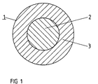
- FIG. 1 shows a superconducting composite body 1 according to the invention with a core 2 made of oxide-ceramic superconductor material and a sheath 3, which preferably consists of silver or a silver alloy.
- a single core conductor with a core made from a BiSrCaCuO superconductor connection (2212 phase) and a silver sheath was produced.
- the cross-section-reducing deformation was carried out by pulling.
- the composite body was coated with a graphite suspension prior to drawing for lubrication and at a temperature above the melting temperature of the oxide ceramic material preheated. The temperature of the last heating stage was about 930 ° C.
- the die was also heated to a temperature of over 500 ° C.
- the composite body was brought from a diameter of 1.46 mm by hot drawing in one go to a diameter of 1.39 mm.
- the core density rose from 68% of the theoretical density to 83% after hot drawing.
- a second pull to a diameter of 1.31 mm brought a further slight increase in the core density to 84%.
- the cross-section-reducing deformation can also be carried out by hot rolling according to the invention with heated rolls.
- the preferred temperature of the rollers, as well as that of the drawing die during drawing, is between 400 and 700 ° C.
Landscapes
- Engineering & Computer Science (AREA)
- Manufacturing & Machinery (AREA)
- Superconductors And Manufacturing Methods Therefor (AREA)
- Compositions Of Oxide Ceramics (AREA)
- Inorganic Compounds Of Heavy Metals (AREA)
Description
- Die Erfindung betrifft ein Verfahren zur Herstellung eines supraleitenden Verbundkörpers durch Einbringen eines oxidkeramischen supraleitenden Materials in eine Hülle, querschnittsreduzierendes Verformen und Wärmebehandeln zur Erholung und Einstellung der Sauerstoffkonzentration sowie einen entsprechenden supraleitenden Verbundkörper.
- Supraleitende Verbundkörper, bei denen ein oxidkeramisches supraleitendes Pulver von einem Hüllmaterial umschlossen ist, sind beispielsweise aus der Veröffentlichung von H. Krauth und A. Szulczyk in METALL, Jg. 45, 1989, Seiten 418 ff bekannt. Durch die Verwendung oxidkeramischer Hochtemperatursupraleiter (HTSL) werden Verbundkörper wie Drähte oder Bänder hergestellt, die auch oberhalb der Temperatur des flüssigen Stickstoffs supraleitend sind. Die hierfür geeigneten Materialien sind an sich bekannt. Hierzu gehören beispielsweise Phasen in den Systemen YBaCuO, BiSrCaCuO und TlBaCaCuO.
- Zur Herstellung technischer Leiter wird oxidkeramisches Pulver beispielsweise in ein Metallrohr eingefüllt, und durch querschnittsreduzierende Verformung wird ein Draht oder ein Band hergestellt. Abschließend wird eine Wärmebehandlung durchgeführt, die der Erzeugung der durchgehend supraleitenden Verbindung durch das HTSL-Material und der Optimierung der kritischen Stromdichte dient.
- Die Hülle besteht in der Regel aus Silber oder Silberlegierungen, da durch diese Materialien die Sauerstoffpermeation durch das Hüllmaterial während der abschließenden Wärmebehandlung zur Einstellung des optimalen Sauerstoffgehaltes gewährleistet ist.
- In SUPERCONDUCTOR SCIENCE and TECHNOLOGY, Bd. 4, Nr. 7, 1991, Seiten 353 bis 354, ist ein derartiger Verbundsupraleiter beschrieben, der durch Kaltverformungschritte auf den vorgesehenen Querschnitt gebracht wird. Im Anschluß daran findet eine Wärmebehandlung unter hydrostatischem Druck in einer Argonatmosphäre statt.
- Um bei der Herstellung der Verbundkörper eine gegenüber diesem Bekannten höhere Fülldichte zu erreichen, kann in die Hüllrohre neben Pulvern auch zu Stangen oder Pellets gepreßtes Pulver oder eine Schmelze gefüllt werden. Bei Verwendung von Pulvern wird eine Fülldichte von ca. 55 %, bezogen auf die theoretische HTSL-Dichte erreicht. Bei Verwendung der zu Stangen oder Pellets gepreßten Pulver werden Fülldichten von etwa 70 % und bei Einfüllen einer Schmelze eine Fülldichte von bis zu 100 % erreicht. Nach der Verformung der gefüllten Rohre zu fertigen Verbunddrähten durch Ziehen oder eine Kombination von Zieh- und Walzschritten beträgt die Kerndichte des oxidkeramischen Supraleitermaterials typischerweise 65 bis 75 % der theoretischen Dichte. Bei der abschließenden Glühung zur Einstellung der supraleitenden Eigenschaften kommt es dann aufgrund des damit verbundenen teilweisen Schmelzens des Kerns zur Bildung großer Poren im HTSL-Kern, die eine stark verringerte kritische Stromdichte zur Folge haben. Diese Poren sind somit unerwünscht und sollen weitgehend vermieden werden.
- Weiterhin ist es aus AMERICAN CERAMIC SOCIETY BULLETIN, Bd. 70, Nr. 5, 1991, S. 813 - 816 bekannt, einen Preßkörper zu verwenden, der unter erhöhter Temperatur durch Strangpressen verformt wird. Beim Strangpressen darf jedoch das Innere des zu pressenden Bolzens nicht flüssig sein, um eine kontrollierte Verformung des Materials zu gewährleisten. Daher ist ausgeführt, daß der Bolzen auf 70 bis 90 % der Schmelztemperatur aufgeheizt wird. Durch Strangpressen hergestelltes Supraleitermaterial ist außerdem in MATERIALS LETTERS, Bd. 10, Nr. 11, 1991, S. 485 - 488 beschrieben. Hier ist als Strangpreßtempertur ein Wert von 1113 K = 840 °C angegeben. Da das Supraleitermaterial in Luft erst ab 890°C teilweise zu schmelzen beginnt, ist auch hier vermieden worden, daß ein Aufschmelzen des Supraleitermaterials bei der Heißverformung auftritt.
- Aufgabe der Erfindung ist es daher, bei einem Supraleiterdraht, bei dem sich das Supraleitermaterial in einer Hülle befindet, ein Verfahren zur Herstellung von oxidkeramischen Verbundkörpern anzugeben, bei denen sich eine erhöhte Kerndichte für den Verbundkörper erreichen läßt und gleichzeitig die Bildung von großen Poren im HTSL-Kern vermieden wird.
- Diese Aufgabe wird in einem Verfahren zur Herstellung eines surpraleitenden Verbundkörpers dadurch gelöst, daß das querschnittsreduzierende Verformen mindestens einen Heißverformungsschritt enthält, bei dem das Supraleitermaterial im geschmolzenen oder partiell geschmolzenen Zustand vorliegt. Ein erfindungsgemäßer supraleitender Verbundkörper weist eine Kerndichte von mehr als 80 % der theoretischen Dichte auf.
- Mit dem erfindungsgemäßen Verfahren wird somit eine Erhöhung der Kerndichte dadurch erreicht, daß ein Heißverformungsschritt vorgesehen ist, bei dem das Supraleitermaterial im geschmolzenen oder partiell geschmolzenen Zustand vorliegt und somit plastisch verformbar ist. Bei diesem Heißverformungsschritt kann es sich insbesondere um ein Heißziehen oder Heißwalzen handeln. Aus der nicht vorveröffentlichten deutschen Patentanmeldung P 41 04 421.5 ist zwar bereits ein Verfahren zur Herstellung eines supraleitenden Verbundkörpers bekannt, bei dem ein Heißwalzen durchgeführt wird; jedoch liegt dort die Temperatur beim Heißwalzen noch unterhalb der Schmelztemperatur des supraleitenden Materials, so daß noch kein partielles Schmelzen desselben auftritt. Speziell angegeben ist dort ein BiSrCaCuO-Supraleitermaterial mit einer Schmelztemperatur von 890 °C. Bei diesem Supraleitermaterial soll die Temperatur beim Heißwalzen zwischen 500 und 800 °C betragen und liegt somit noch deutlich unterhalb der Schmelztemperatur.
- Fig. 1 zeigt einen erfindungsgemäßen supraleitenden Verbundkörper 1 mit einem Kern 2 aus oxidkeramischem Supraleitermaterial und einer Hülle 3, die vorzugsweise aus Silber oder einer Silberlegierung besteht.
- In einem speziellen Ausführungsbeispiel wurde ein Einkernleiter mit einem Kern aus einer BiSrCaCuO-Supraleiterverbindung (2212-Phase) und einer Silberhülle hergestellt. Die querschnittsreduzierende Verformung erfolgte dabei durch Ziehen. Der Verbundkörper wurde vor dem Ziehen zur Schmierung mit einer Graphitsuspension beschichtet und auf eine Temperatur oberhalb der Schmelztemperatur des oxidkeramischen Materials vorgewärmt. Die Temperatur der letzten Erwärmungsstufe betrug hierbei etwa 930 °C. Der Ziehstein wurde ebenfalls aufgeheizt, und zwar auf eine Temperatur von über 500 °C. Mit einer Ziehgeschwindigkeit von 3 bis 4 m pro Minute wurde der Verbundkörper von einem Durchmesser von 1,46 mm durch Heißziehen in einem Zug auf einen Durchmesser von 1,39 mm gebracht. Die Kerndichte stieg dabei von 68 % der theoretischen Dichte auf 83 % nach dem Heißziehen. Ein zweiter Zug auf einen Durchmesser von 1,31 mm brachte eine weitere geringfügige Erhöhung der Kerndichte auf 84 %.
- Analog zu dem beschriebenen Heißziehen kann die querschnittsreduzierende Verformung auch durch erfindungsgemäßes Heißwalzen mit angewärmten Walzen durchgeführt werden. Die bevorzugte Temperatur der Walzen, wie auch des Ziehsteins beim Ziehen, liegt dabei zwischen 400 und 700 °C.
- In Vergleichsversuchen wurden zur Querschnittsreduzierung verschiedene Verfahren durchgeführt und deren Eignung zur Erhöhung der Kerndichte untersucht. Es handelt es sich dabei um das Walzen nach Vorwärmen, jedoch bei Temperaturen unterhalb der Schmelztemperatur des oxidkeramischen Materials, uniaxiales Pressen sowie uniaxiales Heißpressen bei 630 °C und heißisostatisches Pressen bei 750 °C. In keinem Fall wurde eine Erhöhung der Kerndichte mit diesen Vergleichsversuchen erzielt.
- Während in dem Ausführungsbeispiel die Herstellung eines Einkernleiters beschrieben wurde, können mit dem erfindungsgemäßen Verfahren auch an sich bekannte Mehrkernleiter hergestellt werden.
Claims (4)
- Verfahren zur Herstellung eines supraleitenden Verbundkörpers (1) durch- Einbringen eines oxidkeramischen Supraleitermaterials in eine rohrförmige Hülle (3),- ein mindestens zweistufiges querschnittsreduzierendes Verformen, wobei bei mindestens einer Verformungsstufe ein Magnetfeld angelegt wird, und- Wärmebehandeln zur Erholung und Einstellung der Sauerstoffkonzentration,dadurch gekennzeichnet , daß das querschnittsreduzierende Verformen mindestens einen durch Walzen oder Ziehen erfolgenden Heißverformungsschritt bei einer solchen Temperatur enthält, bei der das Supraleitermaterial im geschmolzenen oder partiell geschmolzenen Zustand vorliegt.
- Verfahren nach Anspruch 1, dadurch gekennzeichnet , daß der Ziehstein oder die Walzen angewärmt sind, vorzugsweise auf 400 bis 700°C.
- Verfahren nach einem der vorhergehenden Ansprüche, dadurch gekennzeichnet , daß es sich um einen Mehrkernleiter handelt.
- Supraleitender Verbundkörper (1) nach Anspruch 1, dadurch gekennzeichnet , daß der supraleitende Kern eine Dichte von mehr als 80 % der theoretischen Dichte aufweist.
Applications Claiming Priority (2)
| Application Number | Priority Date | Filing Date | Title |
|---|---|---|---|
| DE4205008A DE4205008A1 (de) | 1992-02-19 | 1992-02-19 | Verfahren zur herstellung eines oxidkeramischen supraleiters mit hoher kerndichte |
| DE4205008 | 1992-02-19 |
Publications (2)
| Publication Number | Publication Date |
|---|---|
| EP0556581A1 EP0556581A1 (de) | 1993-08-25 |
| EP0556581B1 true EP0556581B1 (de) | 1997-04-09 |
Family
ID=6452079
Family Applications (1)
| Application Number | Title | Priority Date | Filing Date |
|---|---|---|---|
| EP93100838A Expired - Lifetime EP0556581B1 (de) | 1992-02-19 | 1993-01-21 | Verfahren zur Herstellung eines oxidkeramischen Supraleiters mit hoher Kerndichte |
Country Status (5)
| Country | Link |
|---|---|
| US (1) | US5898021A (de) |
| EP (1) | EP0556581B1 (de) |
| JP (1) | JPH0612930A (de) |
| DE (2) | DE4205008A1 (de) |
| ES (1) | ES2099297T3 (de) |
Families Citing this family (2)
| Publication number | Priority date | Publication date | Assignee | Title |
|---|---|---|---|---|
| US6370405B1 (en) * | 1997-07-29 | 2002-04-09 | American Superconductor Corporation | Fine uniform filament superconductors |
| CN112466574A (zh) * | 2020-10-30 | 2021-03-09 | 远东电缆有限公司 | 轨道交通高压电缆非金属外护套表面石墨涂覆方法及装置 |
Family Cites Families (5)
| Publication number | Priority date | Publication date | Assignee | Title |
|---|---|---|---|---|
| JPS5659530A (en) * | 1979-10-18 | 1981-05-23 | Toshiba Corp | Manufacture of wire rod having uniform diameter |
| JP2754564B2 (ja) * | 1987-05-01 | 1998-05-20 | 住友電気工業株式会社 | 超電導性複合体の製造方法 |
| DE3885961D1 (de) * | 1987-07-24 | 1994-01-13 | Asea Brown Boveri | Verfahren zur Herstellung eines ummantelten Drahtes aus einem keramischen Hochtemperatur-Supraleiter. |
| DE3873447T2 (de) * | 1987-08-21 | 1993-03-18 | Mitsubishi Materials Corp | Verfahren zur darstellung von supraleitenden materialien. |
| DE4104421A1 (de) * | 1991-02-14 | 1992-08-20 | Vacuumschmelze Gmbh | Oxidkeramischer supraleitender verbundkoerper und verfahren zu seiner herstellung |
-
1992
- 1992-02-19 DE DE4205008A patent/DE4205008A1/de not_active Withdrawn
-
1993
- 1993-01-21 DE DE59306077T patent/DE59306077D1/de not_active Expired - Fee Related
- 1993-01-21 EP EP93100838A patent/EP0556581B1/de not_active Expired - Lifetime
- 1993-01-21 ES ES93100838T patent/ES2099297T3/es not_active Expired - Lifetime
- 1993-02-03 JP JP5040503A patent/JPH0612930A/ja active Pending
- 1993-02-19 US US08/020,304 patent/US5898021A/en not_active Expired - Lifetime
Also Published As
| Publication number | Publication date |
|---|---|
| EP0556581A1 (de) | 1993-08-25 |
| DE59306077D1 (de) | 1997-05-15 |
| US5898021A (en) | 1999-04-27 |
| DE4205008A1 (de) | 1993-08-26 |
| ES2099297T3 (es) | 1997-05-16 |
| JPH0612930A (ja) | 1994-01-21 |
Similar Documents
| Publication | Publication Date | Title |
|---|---|---|
| DE3855912T2 (de) | Supraleitender Draht und Verfahren zu seiner Herstellung | |
| EP0301283B1 (de) | Verfahren zur Herstellung eines ummantelten Drahtes aus einem keramischen Hochtemperatur-Supraleiter | |
| DE3851070T3 (de) | Verfahren zur Herstellung eines Oxid-Verbindungssupraleiterfadens. | |
| DE3855809T2 (de) | Zusammengesetzter Supraleiter | |
| DE68919913T3 (de) | Zusammengesetzter supraleitender Draht und Verfahren zu dessen Herstellung. | |
| DE2052323B2 (de) | Verfahren zur Herstellung eines Supraleiters | |
| DE3855699T2 (de) | Verfahren zur Herstellung eines supraleitenden Gegenstandes sowie diesen Gegenstand verwendende Vorrichtung und Systeme | |
| DE2412573B2 (de) | Verfahren zur herstellung eines unterteilten supraleitenden drahtes | |
| WO1989006053A1 (fr) | Procede de fabrication de fils metalliques ou de bandes en materiaux supraconducteurs a temperature elevee et gaines utilisees pour appliquer le procede | |
| DE3877160T2 (de) | Supraleitender, gemischter draht mit hoher springtemperatur und verfahren zu dessen herstellung. | |
| DE1640573B1 (de) | Verfahren zur hers/tellung von zusammengesetzten supraleitern | |
| DE3124978C2 (de) | Verfahren zur Herstellung von supraleitenden Verbunddrähten | |
| EP0499049B1 (de) | Oxidkeramischer supraleitender Verbundkörper und Verfahren zu seiner Herstellung | |
| EP0357910B1 (de) | Verfahren zur Herstellung eines supraleitenden langgestreckten Gutes aus einem beschichteten gewellten Metallrohr | |
| EP0556581A1 (de) | Verfahren zur Herstellung eines oxidkeramischen Supraleiters mit hoher Kerndichte | |
| DE2835974A1 (de) | Verfahren zur herstellung eines vieladrigen intermetallischen supraleiters | |
| DE3942823C1 (de) | ||
| DE69616868T2 (de) | Verfahren zur Herstellung eines metallimprägnierten Supraleiters | |
| DE3245903C2 (de) | ||
| DE2819242B2 (de) | Verfahren zur Herstellung eines Supraleiters | |
| DE2331919A1 (de) | Verfahren zum herstellen eines supraleiters mit einer supraleitenden intermetallischen verbindung aus wenigstens zwei elementen | |
| DE4113220A1 (de) | Oxidkeramischer supraleitender verbundkoerper fuer wechselfeldanwendungen und verfahren zu seiner herstellung | |
| DE2044660A1 (de) | Verfahren zur Herstellung von Supra leitern | |
| DE2253439C3 (de) | Ternäre Legierung für supraleitende Magneten | |
| DE2413446C2 (de) | Verfahren zur Herstellung eines Supraleiters mit beta-Wolframstruktur |
Legal Events
| Date | Code | Title | Description |
|---|---|---|---|
| PUAI | Public reference made under article 153(3) epc to a published international application that has entered the european phase |
Free format text: ORIGINAL CODE: 0009012 |
|
| AK | Designated contracting states |
Kind code of ref document: A1 Designated state(s): CH DE ES FR GB IT LI |
|
| 17P | Request for examination filed |
Effective date: 19940117 |
|
| 17Q | First examination report despatched |
Effective date: 19950317 |
|
| GRAG | Despatch of communication of intention to grant |
Free format text: ORIGINAL CODE: EPIDOS AGRA |
|
| GRAH | Despatch of communication of intention to grant a patent |
Free format text: ORIGINAL CODE: EPIDOS IGRA |
|
| GRAH | Despatch of communication of intention to grant a patent |
Free format text: ORIGINAL CODE: EPIDOS IGRA |
|
| GRAA | (expected) grant |
Free format text: ORIGINAL CODE: 0009210 |
|
| AK | Designated contracting states |
Kind code of ref document: B1 Designated state(s): CH DE ES FR GB IT LI |
|
| REG | Reference to a national code |
Ref country code: CH Ref legal event code: NV Representative=s name: SIEMENS SCHWEIZ AG Ref country code: CH Ref legal event code: EP |
|
| REF | Corresponds to: |
Ref document number: 59306077 Country of ref document: DE Date of ref document: 19970515 |
|
| REG | Reference to a national code |
Ref country code: ES Ref legal event code: FG2A Ref document number: 2099297 Country of ref document: ES Kind code of ref document: T3 |
|
| GBT | Gb: translation of ep patent filed (gb section 77(6)(a)/1977) |
Effective date: 19970613 |
|
| ET | Fr: translation filed | ||
| PGFP | Annual fee paid to national office [announced via postgrant information from national office to epo] |
Ref country code: ES Payment date: 19980115 Year of fee payment: 6 |
|
| PLBE | No opposition filed within time limit |
Free format text: ORIGINAL CODE: 0009261 |
|
| STAA | Information on the status of an ep patent application or granted ep patent |
Free format text: STATUS: NO OPPOSITION FILED WITHIN TIME LIMIT |
|
| 26N | No opposition filed | ||
| PGFP | Annual fee paid to national office [announced via postgrant information from national office to epo] |
Ref country code: CH Payment date: 19980422 Year of fee payment: 6 |
|
| PG25 | Lapsed in a contracting state [announced via postgrant information from national office to epo] |
Ref country code: ES Free format text: LAPSE BECAUSE OF EXPIRATION OF PROTECTION Effective date: 19990122 |
|
| PG25 | Lapsed in a contracting state [announced via postgrant information from national office to epo] |
Ref country code: LI Free format text: LAPSE BECAUSE OF NON-PAYMENT OF DUE FEES Effective date: 19990131 Ref country code: CH Free format text: LAPSE BECAUSE OF NON-PAYMENT OF DUE FEES Effective date: 19990131 |
|
| REG | Reference to a national code |
Ref country code: CH Ref legal event code: PL |
|
| REG | Reference to a national code |
Ref country code: ES Ref legal event code: FD2A Effective date: 20010601 |
|
| REG | Reference to a national code |
Ref country code: GB Ref legal event code: IF02 |
|
| PGFP | Annual fee paid to national office [announced via postgrant information from national office to epo] |
Ref country code: DE Payment date: 20090220 Year of fee payment: 17 |
|
| PGFP | Annual fee paid to national office [announced via postgrant information from national office to epo] |
Ref country code: GB Payment date: 20090123 Year of fee payment: 17 |
|
| PGFP | Annual fee paid to national office [announced via postgrant information from national office to epo] |
Ref country code: IT Payment date: 20090126 Year of fee payment: 17 |
|
| PGFP | Annual fee paid to national office [announced via postgrant information from national office to epo] |
Ref country code: FR Payment date: 20090120 Year of fee payment: 17 |
|
| GBPC | Gb: european patent ceased through non-payment of renewal fee |
Effective date: 20100121 |
|
| REG | Reference to a national code |
Ref country code: FR Ref legal event code: ST Effective date: 20100930 |
|
| PG25 | Lapsed in a contracting state [announced via postgrant information from national office to epo] |
Ref country code: FR Free format text: LAPSE BECAUSE OF NON-PAYMENT OF DUE FEES Effective date: 20100201 |
|
| PG25 | Lapsed in a contracting state [announced via postgrant information from national office to epo] |
Ref country code: DE Free format text: LAPSE BECAUSE OF NON-PAYMENT OF DUE FEES Effective date: 20100803 |
|
| PG25 | Lapsed in a contracting state [announced via postgrant information from national office to epo] |
Ref country code: GB Free format text: LAPSE BECAUSE OF NON-PAYMENT OF DUE FEES Effective date: 20100121 |
|
| PG25 | Lapsed in a contracting state [announced via postgrant information from national office to epo] |
Ref country code: IT Free format text: LAPSE BECAUSE OF NON-PAYMENT OF DUE FEES Effective date: 20100121 |