EP0554973B1 - Multi-channel trigger dejitter - Google Patents
Multi-channel trigger dejitter Download PDFInfo
- Publication number
- EP0554973B1 EP0554973B1 EP93300030A EP93300030A EP0554973B1 EP 0554973 B1 EP0554973 B1 EP 0554973B1 EP 93300030 A EP93300030 A EP 93300030A EP 93300030 A EP93300030 A EP 93300030A EP 0554973 B1 EP0554973 B1 EP 0554973B1
- Authority
- EP
- European Patent Office
- Prior art keywords
- trigger
- digitized
- time
- dejitter
- sample
- Prior art date
- Legal status (The legal status is an assumption and is not a legal conclusion. Google has not performed a legal analysis and makes no representation as to the accuracy of the status listed.)
- Expired - Lifetime
Links
Images
Classifications
-
- G—PHYSICS
- G01—MEASURING; TESTING
- G01R—MEASURING ELECTRIC VARIABLES; MEASURING MAGNETIC VARIABLES
- G01R13/00—Arrangements for displaying electric variables or waveforms
- G01R13/20—Cathode-ray oscilloscopes
- G01R13/22—Circuits therefor
- G01R13/32—Circuits for displaying non-recurrent functions such as transients; Circuits for triggering; Circuits for synchronisation; Circuits for time-base expansion
Definitions
- the present invention relates to waveform digitizing systems, and more particularly to a multi-channel trigger dejitter technique for digital sampling oscilloscopes and the like that improves the accuracy of the trigger time information for repetitive signals.
- a waveform digitizing system such as a digital sampling oscilloscope, takes discrete periodic samples of multiple analog input signals and either displays them or otherwise stores or transmits them to a remote device, such as a personal computer. If a signal is repetitive and being displayed, it is important that each iteration of the signal be displayed in the same place so that parts of the waveform that are not different do not move around and differences between subsequent iterations are readily apparent.
- the trigger hardware of a digital sampling device ensures that signals are always digitized in the vicinity of a particular event, such as a voltage crossing. Trigger time information is typically provided to much higher resolution than the digitizing sample interval.
- a digital sampling oscilloscope with a digitizing sample interval of 500 picoseconds might provide trigger time resolution of ten picoseconds.
- This allows the display to be horizontally expanded, i.e., "zoomed", either using software interpolation, such as linear or sin(x)/x algorithms, or using equivalent time sampling where the display is filled out over multiple acquisitions. If high resolution trigger time information is not provided accurately, an interpolated display jitters back and forth and an equivalent time sampling display shows vertical noise on edges because of errors in sample time placement with respect to the trigger point.
- EP-A-0335496 discloses a waveform timing alignment system for digital oscilloscopes, having the features of the pre-characterising portion of claim 1 appended hereto.
- an autocorrelation value is generated in connection with a first waveform of a periodic electrical signal, and a first cross-correlation value is generated in connection with the first and a second waveform; these two values are compared to determine whether they differ by more than a preselected tolerance, indicating a timing misalignment, in which case the second waveform is shifted by changing the timing relationship relative to the first waveform.
- a multi-channel trigger dejitter technique uses digitized waveform data from a trigger channel to fine-tune a trigger position in time.
- the horizontal location in the trigger channel where the trigger is expected is located, and the region around the trigger is expanded horizontally.
- the digitized trigger level is extracted and averaged with prior trigger levels to get a running "average trigger” level.
- the expanded waveform is searched for the new average trigger level crossing point, and a time offset is computed from the un-dejittered position. The time offset is used to correct the trigger time so that when the waveforms are subsequently displayed, they are moved horizontally with respect to the trigger by the time offset.
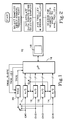
- Fig. 1 is a block diagram of a typical digitizing sampling oscilloscope that uses the multi-channel trigger dejitter technique of the present invention.
- Fig. 2 is a flow chart diagram of the multi-channel trigger dejitter technique of the present invention.
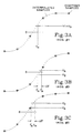
- Figs. 3a, 3b and 3c are graphical views illustrating the operation of the multi-channel trigger dejitter technique of the present invention.
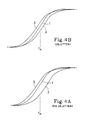
- Figs. 4a and 4b are graphical views illustrating the display of data without and with the multi-channel trigger dejitter technique of the present invention.
- a typical digitizing sampling oscilloscope 10 has multiple input channels Ch1, Ch2, Ch3, Ch4. Separate input signals are applied to each input channel and digitized by respective analog-to-digital converters 11 , 12 , 13 , 14 according to a system clock signal CLK . The digitized samples of the input signals are input to a microprocessor system 16 for further processing. The processed waveforms are presented on an appropriate display device 18 . The portions of the waveforms to be displayed are determined by a trigger signal TRIG generated from one of the input channels, Ch1 in this example.
- a trigger generating circuit 20 receives as inputs the waveform on the one channel and a trigger level signal TRIG _ LEV and a trigger slope signal TRIG _ SLOPE derived from digital signals provided by the microprocessor system 16 . In response the trigger generating circuit 20 generates the trigger signal when the waveform crosses in the specified slope direction the trigger level. The portions of the waveforms displayed are determined by a time interval selected by an operator about the trigger time. Since the sampling clock signal CLK is generally asynchronous with respect to the waveforms, the trigger event may occur at any point between two consecutive samples of the sampling channel.
- Each digitized sample has an amplitude value and a time value determined from the trigger event. Due to the fact that there is noise in the trigger path, the actual trigger level at which the trigger is generated varies, i.e., jitters. Such jitter may result in time errors of the samples by as much as one period of the instrument bandwidth.
- a hardware trigger time Th generated by a first trigger level V1 during a first acquisition of a waveform
- a set of digitized samples for the same channel from which the trigger signal is generated is captured immediately surrounding the hardware trigger.
- a set of interpolated samples is calculated between the digitized samples using an appropriate algorithm, such as a sin(x)/x algorithm.
- the hardware trigger levels are V2 and V3 , and the trigger level for each subsequent acquisition is averaged with up to N prior trigger levels to determine the average trigger level.
- the digitized sample times are adjusted according to the difference between the hardware trigger time and the average trigger time.
- the digitized samples, when aligned in time with the hardware triggers for each acquisition have a definite spread, or jitter, between the different acquisitions.
- jitter When dejitter is used, the different acquisitions are aligned in time with the average triggers, and the resulting jitter is considerably reduced.
- the amount of jitter reduction depends upon the number of averages N , and for a high enough N may be reduced essentially to zero.
- the present invention provides multi-channel trigger dejitter for repetitive waveform acquisitions by using the waveform data itself to determine the appropriate trigger point, and adjusting the digitized samples of the waveforms to an average trigger for each acquisition iteration.
Landscapes
- Physics & Mathematics (AREA)
- General Physics & Mathematics (AREA)
- Analogue/Digital Conversion (AREA)
- Dc Digital Transmission (AREA)
Applications Claiming Priority (2)
| Application Number | Priority Date | Filing Date | Title |
|---|---|---|---|
| US07/828,827 US5352976A (en) | 1992-01-31 | 1992-01-31 | Multi-channel trigger dejitter |
| US828827 | 1992-01-31 |
Publications (3)
| Publication Number | Publication Date |
|---|---|
| EP0554973A2 EP0554973A2 (en) | 1993-08-11 |
| EP0554973A3 EP0554973A3 (enExample) | 1994-01-05 |
| EP0554973B1 true EP0554973B1 (en) | 1998-12-16 |
Family
ID=25252841
Family Applications (1)
| Application Number | Title | Priority Date | Filing Date |
|---|---|---|---|
| EP93300030A Expired - Lifetime EP0554973B1 (en) | 1992-01-31 | 1993-01-05 | Multi-channel trigger dejitter |
Country Status (4)
| Country | Link |
|---|---|
| US (1) | US5352976A (enExample) |
| EP (1) | EP0554973B1 (enExample) |
| JP (1) | JP2592389B2 (enExample) |
| DE (1) | DE69322530T2 (enExample) |
Families Citing this family (12)
| Publication number | Priority date | Publication date | Assignee | Title |
|---|---|---|---|---|
| US6263290B1 (en) * | 1995-02-22 | 2001-07-17 | Michael K. Williams | Process and machine for signal waveform analysis |
| US6269317B1 (en) | 1997-04-30 | 2001-07-31 | Lecroy Corporation | Self-calibration of an oscilloscope using a square-wave test signal |
| JP4547064B2 (ja) * | 1999-03-24 | 2010-09-22 | 株式会社アドバンテスト | A/d変換装置およびキャリブレーション装置 |
| JP4266350B2 (ja) * | 2004-02-12 | 2009-05-20 | 株式会社ルネサステクノロジ | テスト回路 |
| DE102005035473A1 (de) * | 2005-07-28 | 2007-02-01 | Rohde & Schwarz Gmbh & Co. Kg | Verfahren und System zur digitalen Triggerung für Oszilloskope |
| DE102005036855B4 (de) * | 2005-08-04 | 2016-11-17 | Rohde & Schwarz Gmbh & Co. Kg | Verfahren und System zur Triggerung von digitalisierten Signalen |
| US7352167B2 (en) * | 2006-03-24 | 2008-04-01 | Tektronix, Inc. | Digital trigger |
| US8024140B2 (en) * | 2007-08-23 | 2011-09-20 | Amherst Systems Associates, Inc. | Waveform anomoly detection and notification systems and methods |
| EP2651034B1 (en) * | 2012-04-12 | 2014-08-06 | Siemens Aktiengesellschaft | Method for determining a trigger level |
| CN104699435B (zh) * | 2015-02-12 | 2018-01-30 | 深圳市鼎阳科技有限公司 | 一种数字频谱分析仪数据处理方法及装置 |
| JP7154872B2 (ja) * | 2018-08-10 | 2022-10-18 | 横河電機株式会社 | デジタルオシロスコープ及びその制御方法 |
| CN110221572B (zh) * | 2019-04-26 | 2021-04-20 | 北京龙鼎源科技股份有限公司 | 系统控制方法及装置 |
Family Cites Families (7)
| Publication number | Priority date | Publication date | Assignee | Title |
|---|---|---|---|---|
| US4555765A (en) * | 1982-09-14 | 1985-11-26 | Analogic Corporation | Multi-mode oscilloscope trigger with compensating trigger delay |
| JPS6193962A (ja) * | 1984-10-15 | 1986-05-12 | Anritsu Corp | パタ−ントリガ付オシロスコ−プ |
| US4825379A (en) * | 1986-08-29 | 1989-04-25 | Tektronix, Inc. | Method and apparatus for processing waveform records for jitter elimination prior to averaging in determining signal to noise ratio |
| US4779045A (en) * | 1987-01-29 | 1988-10-18 | Tektronix, Inc. | Automatic peak-to-peak amplitude measurement system |
| US4843309A (en) * | 1988-03-21 | 1989-06-27 | Tektronix, Inc. | Waveform timing alignment system for digital oscilloscopes |
| JPH0245767A (ja) * | 1988-06-30 | 1990-02-15 | Tektronix Inc | デジタル・オシロスコープの自動調整方法 |
| JPH0276971A (ja) * | 1988-09-09 | 1990-03-16 | Agency Of Ind Science & Technol | グランドパッキン及びその製造法 |
-
1992
- 1992-01-31 US US07/828,827 patent/US5352976A/en not_active Expired - Fee Related
-
1993
- 1993-01-05 DE DE69322530T patent/DE69322530T2/de not_active Expired - Fee Related
- 1993-01-05 EP EP93300030A patent/EP0554973B1/en not_active Expired - Lifetime
- 1993-01-29 JP JP5032428A patent/JP2592389B2/ja not_active Expired - Lifetime
Also Published As
| Publication number | Publication date |
|---|---|
| JPH0682483A (ja) | 1994-03-22 |
| US5352976A (en) | 1994-10-04 |
| EP0554973A3 (enExample) | 1994-01-05 |
| EP0554973A2 (en) | 1993-08-11 |
| DE69322530D1 (de) | 1999-01-28 |
| JP2592389B2 (ja) | 1997-03-19 |
| DE69322530T2 (de) | 1999-09-02 |
Similar Documents
| Publication | Publication Date | Title |
|---|---|---|
| JP2733746B2 (ja) | ロジック信号表示方法 | |
| US6571186B1 (en) | Method of waveform time stamping for minimizing digitization artifacts in time interval distribution measurements | |
| US6263290B1 (en) | Process and machine for signal waveform analysis | |
| EP0234883B1 (en) | Apparatus and method for random repetitive sampling | |
| US5495168A (en) | Method of signal analysis employing histograms to establish stable, scaled displays in oscilloscopes | |
| EP0554973B1 (en) | Multi-channel trigger dejitter | |
| WO1996026448A9 (en) | Process and machine for signal waveform analysis | |
| US4928251A (en) | Method and apparatus for waveform reconstruction for sampled data system | |
| US7110898B2 (en) | Method for digitally acquiring and compensating signals | |
| JPH0623788B2 (ja) | 波形間不整合補正方法及びデジタル・オシロスコープ | |
| JPS5934164A (ja) | 波形取込装置 | |
| KR100576226B1 (ko) | 인터리브형 디지털 피크 검출기 | |
| EP1118866A1 (en) | Method of estimating phase noise spectral density and jitter in a periodic signal | |
| JPH056151B2 (enExample) | ||
| US6998834B2 (en) | Real-time time drift adjustment for a TDR step stimulus | |
| US6188966B1 (en) | Reconstruction of multi-phase signals from repetitive samples | |
| EP0235250A1 (en) | Harmonic sampling logic analyzer | |
| Stenbakken et al. | Timebase distortion measurements using multiphase sinewaves |
Legal Events
| Date | Code | Title | Description |
|---|---|---|---|
| PUAI | Public reference made under article 153(3) epc to a published international application that has entered the european phase |
Free format text: ORIGINAL CODE: 0009012 |
|
| AK | Designated contracting states |
Kind code of ref document: A2 Designated state(s): DE FR GB |
|
| PUAL | Search report despatched |
Free format text: ORIGINAL CODE: 0009013 |
|
| AK | Designated contracting states |
Kind code of ref document: A3 Designated state(s): DE FR GB |
|
| 17P | Request for examination filed |
Effective date: 19940614 |
|
| 17Q | First examination report despatched |
Effective date: 19970320 |
|
| GRAG | Despatch of communication of intention to grant |
Free format text: ORIGINAL CODE: EPIDOS AGRA |
|
| GRAG | Despatch of communication of intention to grant |
Free format text: ORIGINAL CODE: EPIDOS AGRA |
|
| GRAH | Despatch of communication of intention to grant a patent |
Free format text: ORIGINAL CODE: EPIDOS IGRA |
|
| GRAH | Despatch of communication of intention to grant a patent |
Free format text: ORIGINAL CODE: EPIDOS IGRA |
|
| GRAA | (expected) grant |
Free format text: ORIGINAL CODE: 0009210 |
|
| AK | Designated contracting states |
Kind code of ref document: B1 Designated state(s): DE FR GB |
|
| REF | Corresponds to: |
Ref document number: 69322530 Country of ref document: DE Date of ref document: 19990128 |
|
| ET | Fr: translation filed | ||
| PLBE | No opposition filed within time limit |
Free format text: ORIGINAL CODE: 0009261 |
|
| 26N | No opposition filed | ||
| PGFP | Annual fee paid to national office [announced via postgrant information from national office to epo] |
Ref country code: FR Payment date: 20011210 Year of fee payment: 10 |
|
| PGFP | Annual fee paid to national office [announced via postgrant information from national office to epo] |
Ref country code: GB Payment date: 20011218 Year of fee payment: 10 |
|
| PGFP | Annual fee paid to national office [announced via postgrant information from national office to epo] |
Ref country code: DE Payment date: 20011219 Year of fee payment: 10 |
|
| REG | Reference to a national code |
Ref country code: GB Ref legal event code: IF02 |
|
| PG25 | Lapsed in a contracting state [announced via postgrant information from national office to epo] |
Ref country code: GB Free format text: LAPSE BECAUSE OF NON-PAYMENT OF DUE FEES Effective date: 20030105 |
|
| PG25 | Lapsed in a contracting state [announced via postgrant information from national office to epo] |
Ref country code: DE Free format text: LAPSE BECAUSE OF NON-PAYMENT OF DUE FEES Effective date: 20030801 |
|
| GBPC | Gb: european patent ceased through non-payment of renewal fee |
Effective date: 20030105 |
|
| PG25 | Lapsed in a contracting state [announced via postgrant information from national office to epo] |
Ref country code: FR Free format text: LAPSE BECAUSE OF NON-PAYMENT OF DUE FEES Effective date: 20030930 |
|
| REG | Reference to a national code |
Ref country code: FR Ref legal event code: ST |