EP0540947A2 - Signalverarbeitungssystem für gemischte Signale und Leistungsversorgungsverfahren - Google Patents
Signalverarbeitungssystem für gemischte Signale und Leistungsversorgungsverfahren Download PDFInfo
- Publication number
- EP0540947A2 EP0540947A2 EP92118083A EP92118083A EP0540947A2 EP 0540947 A2 EP0540947 A2 EP 0540947A2 EP 92118083 A EP92118083 A EP 92118083A EP 92118083 A EP92118083 A EP 92118083A EP 0540947 A2 EP0540947 A2 EP 0540947A2
- Authority
- EP
- European Patent Office
- Prior art keywords
- power supply
- supply voltage
- voltage
- subsystem
- digital
- Prior art date
- Legal status (The legal status is an assumption and is not a legal conclusion. Google has not performed a legal analysis and makes no representation as to the accuracy of the status listed.)
- Granted
Links
- 238000012545 processing Methods 0.000 title claims abstract description 47
- 238000000034 method Methods 0.000 title claims description 7
- 230000001105 regulatory effect Effects 0.000 claims abstract description 45
- 230000004044 response Effects 0.000 claims description 11
- 239000000872 buffer Substances 0.000 claims description 9
- 238000005086 pumping Methods 0.000 claims description 6
- 230000033228 biological regulation Effects 0.000 abstract description 5
- 230000005540 biological transmission Effects 0.000 description 49
- 239000003990 capacitor Substances 0.000 description 41
- 239000013642 negative control Substances 0.000 description 15
- 239000013641 positive control Substances 0.000 description 15
- 230000008901 benefit Effects 0.000 description 5
- 230000011664 signaling Effects 0.000 description 5
- 238000013461 design Methods 0.000 description 3
- 229910021420 polycrystalline silicon Inorganic materials 0.000 description 3
- 229920005591 polysilicon Polymers 0.000 description 3
- 230000009471 action Effects 0.000 description 2
- 238000013459 approach Methods 0.000 description 2
- 239000003795 chemical substances by application Substances 0.000 description 2
- 230000006837 decompression Effects 0.000 description 2
- 238000005516 engineering process Methods 0.000 description 2
- 230000008569 process Effects 0.000 description 2
- 230000003044 adaptive effect Effects 0.000 description 1
- OJIJEKBXJYRIBZ-UHFFFAOYSA-N cadmium nickel Chemical compound [Ni].[Cd] OJIJEKBXJYRIBZ-UHFFFAOYSA-N 0.000 description 1
- 230000015556 catabolic process Effects 0.000 description 1
- 230000008859 change Effects 0.000 description 1
- 230000000295 complement effect Effects 0.000 description 1
- 230000006835 compression Effects 0.000 description 1
- 238000007906 compression Methods 0.000 description 1
- 239000000470 constituent Substances 0.000 description 1
- 238000007796 conventional method Methods 0.000 description 1
- 238000006731 degradation reaction Methods 0.000 description 1
- 238000009792 diffusion process Methods 0.000 description 1
- 230000007274 generation of a signal involved in cell-cell signaling Effects 0.000 description 1
- 238000012986 modification Methods 0.000 description 1
- 230000004048 modification Effects 0.000 description 1
- 238000004806 packaging method and process Methods 0.000 description 1
- 230000009467 reduction Effects 0.000 description 1
- 239000004065 semiconductor Substances 0.000 description 1
- 239000002699 waste material Substances 0.000 description 1
Images


Classifications
-
- H—ELECTRICITY
- H02—GENERATION; CONVERSION OR DISTRIBUTION OF ELECTRIC POWER
- H02M—APPARATUS FOR CONVERSION BETWEEN AC AND AC, BETWEEN AC AND DC, OR BETWEEN DC AND DC, AND FOR USE WITH MAINS OR SIMILAR POWER SUPPLY SYSTEMS; CONVERSION OF DC OR AC INPUT POWER INTO SURGE OUTPUT POWER; CONTROL OR REGULATION THEREOF
- H02M3/00—Conversion of DC power input into DC power output
- H02M3/02—Conversion of DC power input into DC power output without intermediate conversion into AC
- H02M3/04—Conversion of DC power input into DC power output without intermediate conversion into AC by static converters
- H02M3/06—Conversion of DC power input into DC power output without intermediate conversion into AC by static converters using resistors or capacitors, e.g. potential divider
- H02M3/07—Conversion of DC power input into DC power output without intermediate conversion into AC by static converters using resistors or capacitors, e.g. potential divider using capacitors charged and discharged alternately by semiconductor devices with control electrode, e.g. charge pumps
-
- G—PHYSICS
- G05—CONTROLLING; REGULATING
- G05F—SYSTEMS FOR REGULATING ELECTRIC OR MAGNETIC VARIABLES
- G05F1/00—Automatic systems in which deviations of an electric quantity from one or more predetermined values are detected at the output of the system and fed back to a device within the system to restore the detected quantity to its predetermined value or values, i.e. retroactive systems
- G05F1/10—Regulating voltage or current
- G05F1/46—Regulating voltage or current wherein the variable actually regulated by the final control device is DC
- G05F1/62—Regulating voltage or current wherein the variable actually regulated by the final control device is DC using bucking or boosting DC sources
-
- H—ELECTRICITY
- H02—GENERATION; CONVERSION OR DISTRIBUTION OF ELECTRIC POWER
- H02M—APPARATUS FOR CONVERSION BETWEEN AC AND AC, BETWEEN AC AND DC, OR BETWEEN DC AND DC, AND FOR USE WITH MAINS OR SIMILAR POWER SUPPLY SYSTEMS; CONVERSION OF DC OR AC INPUT POWER INTO SURGE OUTPUT POWER; CONTROL OR REGULATION THEREOF
- H02M3/00—Conversion of DC power input into DC power output
- H02M3/02—Conversion of DC power input into DC power output without intermediate conversion into AC
- H02M3/04—Conversion of DC power input into DC power output without intermediate conversion into AC by static converters
- H02M3/06—Conversion of DC power input into DC power output without intermediate conversion into AC by static converters using resistors or capacitors, e.g. potential divider
- H02M3/07—Conversion of DC power input into DC power output without intermediate conversion into AC by static converters using resistors or capacitors, e.g. potential divider using capacitors charged and discharged alternately by semiconductor devices with control electrode, e.g. charge pumps
- H02M3/073—Charge pumps of the Schenkel-type
-
- H—ELECTRICITY
- H03—ELECTRONIC CIRCUITRY
- H03M—CODING; DECODING; CODE CONVERSION IN GENERAL
- H03M1/00—Analogue/digital conversion; Digital/analogue conversion
Definitions
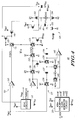
- Integrating portion 113 adjusts the conductivity of transistor 151 to further increase the accuracy of V DD .
- Integrating portion 113 is a switched capacitor (switched-C) differential integrator which integrates a difference between V PDD and V REF over time. While slower in response than proportional portion 112, integrating portion 113 includes the history of the signal levels, which eventually cancels the offset error of proportional portion 112.
- Amplifier 130 is a unity-gain differential amplifier which buffers signal V PDD and keeps integrating portion 113 from affecting the operation of proportional portion 112. At power up, signals PCNTL and ICNTL are low in potential, making transistors 150 and 151 strongly conductive to reach the desired value of V DD quicker.
- Resistor string circuit 210 performs the first function of providing signal V PDD .
- V PDD V DD (R215/(R211 + R214 + R215)) where R211 is the resistance of resistor 211, R214 is the resistance of resistor 214, and R215 is the resistance of resistor 215.
Landscapes
- Engineering & Computer Science (AREA)
- Power Engineering (AREA)
- Physics & Mathematics (AREA)
- Electromagnetism (AREA)
- General Physics & Mathematics (AREA)
- Radar, Positioning & Navigation (AREA)
- Automation & Control Theory (AREA)
- Theoretical Computer Science (AREA)
- Dc-Dc Converters (AREA)
- Mobile Radio Communication Systems (AREA)
- Analogue/Digital Conversion (AREA)
Applications Claiming Priority (2)
| Application Number | Priority Date | Filing Date | Title |
|---|---|---|---|
| US78897791A | 1991-11-07 | 1991-11-07 | |
| US788977 | 1991-11-07 |
Publications (3)
| Publication Number | Publication Date |
|---|---|
| EP0540947A2 true EP0540947A2 (de) | 1993-05-12 |
| EP0540947A3 EP0540947A3 (en) | 1995-02-22 |
| EP0540947B1 EP0540947B1 (de) | 1998-01-21 |
Family
ID=25146180
Family Applications (1)
| Application Number | Title | Priority Date | Filing Date |
|---|---|---|---|
| EP92118083A Expired - Lifetime EP0540947B1 (de) | 1991-11-07 | 1992-10-22 | Signalverarbeitungssystem für gemischte Signale und Leistungsversorgungsverfahren |
Country Status (5)
| Country | Link |
|---|---|
| US (1) | US6034562A (de) |
| EP (1) | EP0540947B1 (de) |
| JP (1) | JP2805181B2 (de) |
| KR (1) | KR0185735B1 (de) |
| CN (1) | CN1075690C (de) |
Cited By (1)
| Publication number | Priority date | Publication date | Assignee | Title |
|---|---|---|---|---|
| WO2000019588A1 (en) * | 1998-09-25 | 2000-04-06 | Conexant Systems, Inc. | Method and apparatus for deriving power from a clock signal coupled through capacitors |
Families Citing this family (16)
| Publication number | Priority date | Publication date | Assignee | Title |
|---|---|---|---|---|
| US6243772B1 (en) * | 1997-01-31 | 2001-06-05 | Sharewave, Inc. | Method and system for coupling a personal computer with an appliance unit via a wireless communication link to provide an output display presentation |
| US6320797B1 (en) * | 1999-02-24 | 2001-11-20 | Micron Technology, Inc. | Method and circuit for regulating the output voltage from a charge pump circuit, and memory device using same |
| US6310789B1 (en) | 1999-06-25 | 2001-10-30 | The Procter & Gamble Company | Dynamically-controlled, intrinsically regulated charge pump power converter |
| CN100364222C (zh) | 1999-06-25 | 2008-01-23 | 伊利诺伊大学评议会 | 电池和电源管理电路 |
| US6392470B1 (en) * | 2000-09-29 | 2002-05-21 | International Business Machines Corporation | Bandgap reference voltage startup circuit |
| GB2373654B (en) * | 2001-03-21 | 2005-02-09 | Fujitsu Ltd | Reducing jitter in mixed-signal integrated circuit devices |
| US6452419B1 (en) * | 2001-04-12 | 2002-09-17 | Power Signal Technologies, Inc. | Control circuit having stacked IC logic |
| US6812739B2 (en) * | 2002-09-26 | 2004-11-02 | International Business Machines Corporation | Method of transparently reducing power consumption of a high-speed communication link |
| US7577039B2 (en) * | 2005-11-16 | 2009-08-18 | Montage Technology Group, Ltd. | Memory interface to bridge memory buses |
| US7368950B2 (en) * | 2005-11-16 | 2008-05-06 | Montage Technology Group Limited | High speed transceiver with low power consumption |
| US20090319260A1 (en) * | 2008-06-19 | 2009-12-24 | Hongwei Kong | Method and system for audio transmit processing in an audio codec |
| US8816659B2 (en) | 2010-08-06 | 2014-08-26 | Peregrine Semiconductor Corporation | Low-noise high efficiency bias generation circuits and method |
| US8169257B2 (en) * | 2009-11-18 | 2012-05-01 | Freescale Semiconductor, Inc. | System and method for communicating between multiple voltage tiers |
| US8476962B2 (en) * | 2009-11-18 | 2013-07-02 | Freescale Semiconductor, Inc. | System having multiple voltage tiers and method therefor |
| JP5566211B2 (ja) * | 2010-07-15 | 2014-08-06 | ローム株式会社 | スイッチドキャパシタ型d/aコンバータ |
| US9002447B2 (en) | 2013-03-14 | 2015-04-07 | Medtronic, Inc. | Implantable medical device having power supply for generating a regulated power supply |
Family Cites Families (21)
| Publication number | Priority date | Publication date | Assignee | Title |
|---|---|---|---|---|
| US4188585A (en) * | 1978-03-16 | 1980-02-12 | Cincinnati Electronics Corporation | Synchronized receiver power system |
| US4356412A (en) * | 1979-03-05 | 1982-10-26 | Motorola, Inc. | Substrate bias regulator |
| JPS576384A (en) * | 1980-06-13 | 1982-01-13 | Hitachi Ltd | Power source circuit and electronic watch using this |
| JPS5731333A (en) * | 1980-07-31 | 1982-02-19 | Suwa Seikosha Kk | Power source circuit system |
| US4485433A (en) * | 1982-12-22 | 1984-11-27 | Ncr Corporation | Integrated circuit dual polarity high voltage multiplier for extended operating temperature range |
| JPS59153331A (ja) * | 1983-02-21 | 1984-09-01 | Toshiba Corp | 半導体装置 |
| US4670673A (en) * | 1985-02-19 | 1987-06-02 | Advanced Micro Devices, Inc. | Multilevel differential ECL/CML gate circuit |
| JPH0683085B2 (ja) * | 1986-03-26 | 1994-10-19 | ソニー株式会社 | 送信機 |
| JP2721151B2 (ja) * | 1986-04-01 | 1998-03-04 | 株式会社東芝 | 半導体集積回路装置 |
| JPS63290159A (ja) * | 1987-05-20 | 1988-11-28 | Matsushita Electric Ind Co Ltd | 昇圧回路 |
| JPS6445157A (en) * | 1987-08-13 | 1989-02-17 | Toshiba Corp | Semiconductor integrated circuit |
| US4868908A (en) * | 1988-10-18 | 1989-09-19 | Ventritex | Power supply down-conversion, regulation and low battery detection system |
| US4947061A (en) * | 1989-02-13 | 1990-08-07 | At&T Bell Laboratories | CMOS to ECL output buffer circuit |
| JPH02215154A (ja) * | 1989-02-16 | 1990-08-28 | Toshiba Corp | 電圧制御回路 |
| JPH02118440U (de) * | 1989-03-10 | 1990-09-21 | ||
| US5043605A (en) * | 1989-06-26 | 1991-08-27 | At&T Bell Laboratories | CMOS to ECL output buffer |
| US5021680A (en) * | 1989-07-31 | 1991-06-04 | Advanced Micro Devices, Inc. | Voltage supply circuit for programming circuits of programmable logic arrays |
| US5066873A (en) * | 1989-12-04 | 1991-11-19 | Altera Corporation | Integrated circuits with reduced switching noise |
| US5063304A (en) * | 1990-04-27 | 1991-11-05 | Texas Instruments Incorporated | Integrated circuit with improved on-chip power supply control |
| US5045772A (en) * | 1990-10-01 | 1991-09-03 | Altera Corporation | Reference voltage generator |
| US5140196A (en) * | 1991-04-15 | 1992-08-18 | Motorola, Inc. | Variable level translator |
-
1992
- 1992-10-08 CN CN92111375A patent/CN1075690C/zh not_active Expired - Lifetime
- 1992-10-22 EP EP92118083A patent/EP0540947B1/de not_active Expired - Lifetime
- 1992-11-04 JP JP4319350A patent/JP2805181B2/ja not_active Expired - Lifetime
- 1992-11-06 KR KR1019920020889A patent/KR0185735B1/ko not_active Expired - Lifetime
-
1995
- 1995-05-17 US US08/442,742 patent/US6034562A/en not_active Expired - Lifetime
Cited By (2)
| Publication number | Priority date | Publication date | Assignee | Title |
|---|---|---|---|---|
| WO2000019588A1 (en) * | 1998-09-25 | 2000-04-06 | Conexant Systems, Inc. | Method and apparatus for deriving power from a clock signal coupled through capacitors |
| US6389135B1 (en) | 1998-09-25 | 2002-05-14 | Conexant Systems, Inc. | Method and apparatus for deriving power from a clock signal coupled through capacitors |
Also Published As
| Publication number | Publication date |
|---|---|
| JPH05235820A (ja) | 1993-09-10 |
| KR0185735B1 (ko) | 1999-05-15 |
| HK1007245A1 (en) | 1999-04-01 |
| EP0540947A3 (en) | 1995-02-22 |
| JP2805181B2 (ja) | 1998-09-30 |
| CN1075690C (zh) | 2001-11-28 |
| US6034562A (en) | 2000-03-07 |
| KR930011434A (ko) | 1993-06-24 |
| CN1073062A (zh) | 1993-06-09 |
| EP0540947B1 (de) | 1998-01-21 |
Similar Documents
| Publication | Publication Date | Title |
|---|---|---|
| EP0540948B1 (de) | Gesteuerte Ladungspumpe und Steuerverfahren | |
| EP0540947B1 (de) | Signalverarbeitungssystem für gemischte Signale und Leistungsversorgungsverfahren | |
| US6735456B2 (en) | Power-saving mode for portable communication devices | |
| JP2938958B2 (ja) | Dc―dcコンバータ | |
| US5642063A (en) | Current-saving detection for input signal level exceeding a threshold value | |
| US5949233A (en) | Circuit for detecting overcharging and overdischarging | |
| EP0326968A1 (de) | Steuerschaltung mit elektrischen Kenndaten, veränderbar in Abhängigkeit vom Lastwiderstand | |
| EP1247426A1 (de) | Digitales hörhilfegerät mit spannungswandler | |
| US5166630A (en) | Low current switched capacitor circuit | |
| US6586967B2 (en) | Integrated circuit device having data signal output at voltage level of the device coupled thereto | |
| ATE177268T1 (de) | Ladesteuerungsschaltung für eine zweitbatterie | |
| JP4221665B2 (ja) | 携帯端末装置 | |
| EP0622895B1 (de) | Kommunikationsapparat mit Leistungsverstärker | |
| EP0700165A2 (de) | Portables Funkgerät | |
| US20040135598A1 (en) | Input circuit | |
| US6020727A (en) | Setting of a linear regulator to stand-by | |
| HK1007245B (en) | Mixed signal processing system and method for powering same | |
| WO1999033168A1 (en) | Low voltage transistor biasing | |
| US5515431A (en) | Speakerphone device with auxiliary circuit for eliminating clicking at power-on | |
| US5977657A (en) | Electric power supply device for producing a plurality of voltages and apparatus comprising such a device | |
| JPH0213988B2 (de) | ||
| US5880619A (en) | Low power precision voltage splitter | |
| KR100312338B1 (ko) | 이동 통신 단말기의 전력증폭기 입력 전압 제어 회로 | |
| US5963095A (en) | Amplifier circuit, a transmitter and a wireless telephone | |
| JPH03278741A (ja) | インターフェイスicのスタンバイ回路 |
Legal Events
| Date | Code | Title | Description |
|---|---|---|---|
| PUAI | Public reference made under article 153(3) epc to a published international application that has entered the european phase |
Free format text: ORIGINAL CODE: 0009012 |
|
| AK | Designated contracting states |
Kind code of ref document: A2 Designated state(s): FR GB |
|
| PUAL | Search report despatched |
Free format text: ORIGINAL CODE: 0009013 |
|
| AK | Designated contracting states |
Kind code of ref document: A3 Designated state(s): FR GB |
|
| 17P | Request for examination filed |
Effective date: 19950822 |
|
| 17Q | First examination report despatched |
Effective date: 19960105 |
|
| GRAG | Despatch of communication of intention to grant |
Free format text: ORIGINAL CODE: EPIDOS AGRA |
|
| GRAG | Despatch of communication of intention to grant |
Free format text: ORIGINAL CODE: EPIDOS AGRA |
|
| GRAH | Despatch of communication of intention to grant a patent |
Free format text: ORIGINAL CODE: EPIDOS IGRA |
|
| GRAH | Despatch of communication of intention to grant a patent |
Free format text: ORIGINAL CODE: EPIDOS IGRA |
|
| GRAA | (expected) grant |
Free format text: ORIGINAL CODE: 0009210 |
|
| AK | Designated contracting states |
Kind code of ref document: B1 Designated state(s): FR GB |
|
| ET | Fr: translation filed | ||
| PLBE | No opposition filed within time limit |
Free format text: ORIGINAL CODE: 0009261 |
|
| STAA | Information on the status of an ep patent application or granted ep patent |
Free format text: STATUS: NO OPPOSITION FILED WITHIN TIME LIMIT |
|
| 26N | No opposition filed | ||
| REG | Reference to a national code |
Ref country code: GB Ref legal event code: IF02 |
|
| REG | Reference to a national code |
Ref country code: GB Ref legal event code: 732E |
|
| REG | Reference to a national code |
Ref country code: FR Ref legal event code: TP |
|
| PGFP | Annual fee paid to national office [announced via postgrant information from national office to epo] |
Ref country code: GB Payment date: 20100923 Year of fee payment: 19 |
|
| PGFP | Annual fee paid to national office [announced via postgrant information from national office to epo] |
Ref country code: FR Payment date: 20111028 Year of fee payment: 20 |
|
| REG | Reference to a national code |
Ref country code: GB Ref legal event code: PE20 Expiry date: 20121021 |
|
| PG25 | Lapsed in a contracting state [announced via postgrant information from national office to epo] |
Ref country code: GB Free format text: LAPSE BECAUSE OF EXPIRATION OF PROTECTION Effective date: 20121021 |