EP0537364B1 - Apparatus and method for manufacturing semiconductor device - Google Patents
Apparatus and method for manufacturing semiconductor device Download PDFInfo
- Publication number
- EP0537364B1 EP0537364B1 EP92908472A EP92908472A EP0537364B1 EP 0537364 B1 EP0537364 B1 EP 0537364B1 EP 92908472 A EP92908472 A EP 92908472A EP 92908472 A EP92908472 A EP 92908472A EP 0537364 B1 EP0537364 B1 EP 0537364B1
- Authority
- EP
- European Patent Office
- Prior art keywords
- wafer
- film
- temperature
- processing
- gas
- Prior art date
- Legal status (The legal status is an assumption and is not a legal conclusion. Google has not performed a legal analysis and makes no representation as to the accuracy of the status listed.)
- Expired - Lifetime
Links
Images





Classifications
-
- C—CHEMISTRY; METALLURGY
- C23—COATING METALLIC MATERIAL; COATING MATERIAL WITH METALLIC MATERIAL; CHEMICAL SURFACE TREATMENT; DIFFUSION TREATMENT OF METALLIC MATERIAL; COATING BY VACUUM EVAPORATION, BY SPUTTERING, BY ION IMPLANTATION OR BY CHEMICAL VAPOUR DEPOSITION, IN GENERAL; INHIBITING CORROSION OF METALLIC MATERIAL OR INCRUSTATION IN GENERAL
- C23C—COATING METALLIC MATERIAL; COATING MATERIAL WITH METALLIC MATERIAL; SURFACE TREATMENT OF METALLIC MATERIAL BY DIFFUSION INTO THE SURFACE, BY CHEMICAL CONVERSION OR SUBSTITUTION; COATING BY VACUUM EVAPORATION, BY SPUTTERING, BY ION IMPLANTATION OR BY CHEMICAL VAPOUR DEPOSITION, IN GENERAL
- C23C16/00—Chemical coating by decomposition of gaseous compounds, without leaving reaction products of surface material in the coating, i.e. chemical vapour deposition [CVD] processes
- C23C16/44—Chemical coating by decomposition of gaseous compounds, without leaving reaction products of surface material in the coating, i.e. chemical vapour deposition [CVD] processes characterised by the method of coating
- C23C16/48—Chemical coating by decomposition of gaseous compounds, without leaving reaction products of surface material in the coating, i.e. chemical vapour deposition [CVD] processes characterised by the method of coating by irradiation, e.g. photolysis, radiolysis, particle radiation
- C23C16/481—Chemical coating by decomposition of gaseous compounds, without leaving reaction products of surface material in the coating, i.e. chemical vapour deposition [CVD] processes characterised by the method of coating by irradiation, e.g. photolysis, radiolysis, particle radiation by radiant heating of the substrate
-
- C—CHEMISTRY; METALLURGY
- C23—COATING METALLIC MATERIAL; COATING MATERIAL WITH METALLIC MATERIAL; CHEMICAL SURFACE TREATMENT; DIFFUSION TREATMENT OF METALLIC MATERIAL; COATING BY VACUUM EVAPORATION, BY SPUTTERING, BY ION IMPLANTATION OR BY CHEMICAL VAPOUR DEPOSITION, IN GENERAL; INHIBITING CORROSION OF METALLIC MATERIAL OR INCRUSTATION IN GENERAL
- C23C—COATING METALLIC MATERIAL; COATING MATERIAL WITH METALLIC MATERIAL; SURFACE TREATMENT OF METALLIC MATERIAL BY DIFFUSION INTO THE SURFACE, BY CHEMICAL CONVERSION OR SUBSTITUTION; COATING BY VACUUM EVAPORATION, BY SPUTTERING, BY ION IMPLANTATION OR BY CHEMICAL VAPOUR DEPOSITION, IN GENERAL
- C23C16/00—Chemical coating by decomposition of gaseous compounds, without leaving reaction products of surface material in the coating, i.e. chemical vapour deposition [CVD] processes
- C23C16/44—Chemical coating by decomposition of gaseous compounds, without leaving reaction products of surface material in the coating, i.e. chemical vapour deposition [CVD] processes characterised by the method of coating
- C23C16/54—Apparatus specially adapted for continuous coating
-
- C—CHEMISTRY; METALLURGY
- C23—COATING METALLIC MATERIAL; COATING MATERIAL WITH METALLIC MATERIAL; CHEMICAL SURFACE TREATMENT; DIFFUSION TREATMENT OF METALLIC MATERIAL; COATING BY VACUUM EVAPORATION, BY SPUTTERING, BY ION IMPLANTATION OR BY CHEMICAL VAPOUR DEPOSITION, IN GENERAL; INHIBITING CORROSION OF METALLIC MATERIAL OR INCRUSTATION IN GENERAL
- C23C—COATING METALLIC MATERIAL; COATING MATERIAL WITH METALLIC MATERIAL; SURFACE TREATMENT OF METALLIC MATERIAL BY DIFFUSION INTO THE SURFACE, BY CHEMICAL CONVERSION OR SUBSTITUTION; COATING BY VACUUM EVAPORATION, BY SPUTTERING, BY ION IMPLANTATION OR BY CHEMICAL VAPOUR DEPOSITION, IN GENERAL
- C23C16/00—Chemical coating by decomposition of gaseous compounds, without leaving reaction products of surface material in the coating, i.e. chemical vapour deposition [CVD] processes
- C23C16/56—After-treatment
-
- H—ELECTRICITY
- H10—SEMICONDUCTOR DEVICES; ELECTRIC SOLID-STATE DEVICES NOT OTHERWISE PROVIDED FOR
- H10P—GENERIC PROCESSES OR APPARATUS FOR THE MANUFACTURE OR TREATMENT OF DEVICES COVERED BY CLASS H10
- H10P14/00—Formation of materials, e.g. in the shape of layers or pillars
- H10P14/60—Formation of materials, e.g. in the shape of layers or pillars of insulating materials
- H10P14/65—Formation of materials, e.g. in the shape of layers or pillars of insulating materials characterised by treatments performed before or after the formation of the materials
- H10P14/6502—Formation of materials, e.g. in the shape of layers or pillars of insulating materials characterised by treatments performed before or after the formation of the materials of treatments performed before formation of the materials
- H10P14/6506—Formation of intermediate materials
-
- H—ELECTRICITY
- H10—SEMICONDUCTOR DEVICES; ELECTRIC SOLID-STATE DEVICES NOT OTHERWISE PROVIDED FOR
- H10P—GENERIC PROCESSES OR APPARATUS FOR THE MANUFACTURE OR TREATMENT OF DEVICES COVERED BY CLASS H10
- H10P14/00—Formation of materials, e.g. in the shape of layers or pillars
- H10P14/60—Formation of materials, e.g. in the shape of layers or pillars of insulating materials
- H10P14/65—Formation of materials, e.g. in the shape of layers or pillars of insulating materials characterised by treatments performed before or after the formation of the materials
- H10P14/6516—Formation of materials, e.g. in the shape of layers or pillars of insulating materials characterised by treatments performed before or after the formation of the materials of treatments performed after formation of the materials
- H10P14/6529—Formation of materials, e.g. in the shape of layers or pillars of insulating materials characterised by treatments performed before or after the formation of the materials of treatments performed after formation of the materials by exposure to a gas or vapour
-
- H—ELECTRICITY
- H10—SEMICONDUCTOR DEVICES; ELECTRIC SOLID-STATE DEVICES NOT OTHERWISE PROVIDED FOR
- H10P—GENERIC PROCESSES OR APPARATUS FOR THE MANUFACTURE OR TREATMENT OF DEVICES COVERED BY CLASS H10
- H10P14/00—Formation of materials, e.g. in the shape of layers or pillars
- H10P14/60—Formation of materials, e.g. in the shape of layers or pillars of insulating materials
- H10P14/65—Formation of materials, e.g. in the shape of layers or pillars of insulating materials characterised by treatments performed before or after the formation of the materials
- H10P14/6516—Formation of materials, e.g. in the shape of layers or pillars of insulating materials characterised by treatments performed before or after the formation of the materials of treatments performed after formation of the materials
- H10P14/6536—Formation of materials, e.g. in the shape of layers or pillars of insulating materials characterised by treatments performed before or after the formation of the materials of treatments performed after formation of the materials by exposure to radiation, e.g. visible light
-
- H—ELECTRICITY
- H10—SEMICONDUCTOR DEVICES; ELECTRIC SOLID-STATE DEVICES NOT OTHERWISE PROVIDED FOR
- H10P—GENERIC PROCESSES OR APPARATUS FOR THE MANUFACTURE OR TREATMENT OF DEVICES COVERED BY CLASS H10
- H10P14/00—Formation of materials, e.g. in the shape of layers or pillars
- H10P14/60—Formation of materials, e.g. in the shape of layers or pillars of insulating materials
- H10P14/65—Formation of materials, e.g. in the shape of layers or pillars of insulating materials characterised by treatments performed before or after the formation of the materials
- H10P14/6516—Formation of materials, e.g. in the shape of layers or pillars of insulating materials characterised by treatments performed before or after the formation of the materials of treatments performed after formation of the materials
- H10P14/6536—Formation of materials, e.g. in the shape of layers or pillars of insulating materials characterised by treatments performed before or after the formation of the materials of treatments performed after formation of the materials by exposure to radiation, e.g. visible light
- H10P14/6538—Formation of materials, e.g. in the shape of layers or pillars of insulating materials characterised by treatments performed before or after the formation of the materials of treatments performed after formation of the materials by exposure to radiation, e.g. visible light by exposure to UV light
-
- H—ELECTRICITY
- H10—SEMICONDUCTOR DEVICES; ELECTRIC SOLID-STATE DEVICES NOT OTHERWISE PROVIDED FOR
- H10P—GENERIC PROCESSES OR APPARATUS FOR THE MANUFACTURE OR TREATMENT OF DEVICES COVERED BY CLASS H10
- H10P14/00—Formation of materials, e.g. in the shape of layers or pillars
- H10P14/60—Formation of materials, e.g. in the shape of layers or pillars of insulating materials
- H10P14/69—Inorganic materials
- H10P14/692—Inorganic materials composed of oxides, glassy oxides or oxide-based glasses
- H10P14/6921—Inorganic materials composed of oxides, glassy oxides or oxide-based glasses containing silicon
- H10P14/6922—Inorganic materials composed of oxides, glassy oxides or oxide-based glasses containing silicon the material containing Si, O and at least one of H, N, C, F or other non-metal elements, e.g. SiOC, SiOC:H or SiONC
- H10P14/6923—Inorganic materials composed of oxides, glassy oxides or oxide-based glasses containing silicon the material containing Si, O and at least one of H, N, C, F or other non-metal elements, e.g. SiOC, SiOC:H or SiONC the material being boron or phosphorus doped silicon oxides, e.g. BPSG, BSG or PSG
-
- H—ELECTRICITY
- H10—SEMICONDUCTOR DEVICES; ELECTRIC SOLID-STATE DEVICES NOT OTHERWISE PROVIDED FOR
- H10P—GENERIC PROCESSES OR APPARATUS FOR THE MANUFACTURE OR TREATMENT OF DEVICES COVERED BY CLASS H10
- H10P72/00—Handling or holding of wafers, substrates or devices during manufacture or treatment thereof
- H10P72/04—Apparatus for manufacture or treatment
- H10P72/0402—Apparatus for fluid treatment
-
- H—ELECTRICITY
- H10—SEMICONDUCTOR DEVICES; ELECTRIC SOLID-STATE DEVICES NOT OTHERWISE PROVIDED FOR
- H10P—GENERIC PROCESSES OR APPARATUS FOR THE MANUFACTURE OR TREATMENT OF DEVICES COVERED BY CLASS H10
- H10P72/00—Handling or holding of wafers, substrates or devices during manufacture or treatment thereof
- H10P72/04—Apparatus for manufacture or treatment
- H10P72/0431—Apparatus for thermal treatment
- H10P72/0432—Apparatus for thermal treatment mainly by conduction
-
- H—ELECTRICITY
- H10—SEMICONDUCTOR DEVICES; ELECTRIC SOLID-STATE DEVICES NOT OTHERWISE PROVIDED FOR
- H10P—GENERIC PROCESSES OR APPARATUS FOR THE MANUFACTURE OR TREATMENT OF DEVICES COVERED BY CLASS H10
- H10P72/00—Handling or holding of wafers, substrates or devices during manufacture or treatment thereof
- H10P72/04—Apparatus for manufacture or treatment
- H10P72/0451—Apparatus for manufacturing or treating in a plurality of work-stations
- H10P72/0452—Apparatus for manufacturing or treating in a plurality of work-stations characterised by the layout of the process chambers
- H10P72/0454—Apparatus for manufacturing or treating in a plurality of work-stations characterised by the layout of the process chambers surrounding a central transfer chamber
-
- H—ELECTRICITY
- H10—SEMICONDUCTOR DEVICES; ELECTRIC SOLID-STATE DEVICES NOT OTHERWISE PROVIDED FOR
- H10P—GENERIC PROCESSES OR APPARATUS FOR THE MANUFACTURE OR TREATMENT OF DEVICES COVERED BY CLASS H10
- H10P72/00—Handling or holding of wafers, substrates or devices during manufacture or treatment thereof
- H10P72/04—Apparatus for manufacture or treatment
- H10P72/0451—Apparatus for manufacturing or treating in a plurality of work-stations
- H10P72/0468—Apparatus for manufacturing or treating in a plurality of work-stations comprising a chamber adapted to a particular process
-
- H—ELECTRICITY
- H10—SEMICONDUCTOR DEVICES; ELECTRIC SOLID-STATE DEVICES NOT OTHERWISE PROVIDED FOR
- H10P—GENERIC PROCESSES OR APPARATUS FOR THE MANUFACTURE OR TREATMENT OF DEVICES COVERED BY CLASS H10
- H10P95/00—Generic processes or apparatus for manufacture or treatments not covered by the other groups of this subclass
-
- H—ELECTRICITY
- H10—SEMICONDUCTOR DEVICES; ELECTRIC SOLID-STATE DEVICES NOT OTHERWISE PROVIDED FOR
- H10P—GENERIC PROCESSES OR APPARATUS FOR THE MANUFACTURE OR TREATMENT OF DEVICES COVERED BY CLASS H10
- H10P95/00—Generic processes or apparatus for manufacture or treatments not covered by the other groups of this subclass
- H10P95/90—Thermal treatments, e.g. annealing or sintering
-
- H—ELECTRICITY
- H10—SEMICONDUCTOR DEVICES; ELECTRIC SOLID-STATE DEVICES NOT OTHERWISE PROVIDED FOR
- H10W—GENERIC PACKAGES, INTERCONNECTIONS, CONNECTORS OR OTHER CONSTRUCTIONAL DETAILS OF DEVICES COVERED BY CLASS H10
- H10W20/00—Interconnections in chips, wafers or substrates
- H10W20/01—Manufacture or treatment
- H10W20/071—Manufacture or treatment of dielectric parts thereof
- H10W20/092—Manufacture or treatment of dielectric parts thereof by smoothing the dielectric parts
-
- H—ELECTRICITY
- H10—SEMICONDUCTOR DEVICES; ELECTRIC SOLID-STATE DEVICES NOT OTHERWISE PROVIDED FOR
- H10P—GENERIC PROCESSES OR APPARATUS FOR THE MANUFACTURE OR TREATMENT OF DEVICES COVERED BY CLASS H10
- H10P14/00—Formation of materials, e.g. in the shape of layers or pillars
- H10P14/60—Formation of materials, e.g. in the shape of layers or pillars of insulating materials
- H10P14/63—Formation of materials, e.g. in the shape of layers or pillars of insulating materials characterised by the formation processes
- H10P14/6326—Deposition processes
- H10P14/6328—Deposition from the gas or vapour phase
- H10P14/6334—Deposition from the gas or vapour phase using decomposition or reaction of gaseous or vapour phase compounds, i.e. chemical vapour deposition
-
- H—ELECTRICITY
- H10—SEMICONDUCTOR DEVICES; ELECTRIC SOLID-STATE DEVICES NOT OTHERWISE PROVIDED FOR
- H10P—GENERIC PROCESSES OR APPARATUS FOR THE MANUFACTURE OR TREATMENT OF DEVICES COVERED BY CLASS H10
- H10P14/00—Formation of materials, e.g. in the shape of layers or pillars
- H10P14/60—Formation of materials, e.g. in the shape of layers or pillars of insulating materials
- H10P14/63—Formation of materials, e.g. in the shape of layers or pillars of insulating materials characterised by the formation processes
- H10P14/6326—Deposition processes
- H10P14/6328—Deposition from the gas or vapour phase
- H10P14/6334—Deposition from the gas or vapour phase using decomposition or reaction of gaseous or vapour phase compounds, i.e. chemical vapour deposition
- H10P14/6339—Deposition from the gas or vapour phase using decomposition or reaction of gaseous or vapour phase compounds, i.e. chemical vapour deposition deposition by cyclic CVD, e.g. ALD, ALE or pulsed CVD
-
- Y—GENERAL TAGGING OF NEW TECHNOLOGICAL DEVELOPMENTS; GENERAL TAGGING OF CROSS-SECTIONAL TECHNOLOGIES SPANNING OVER SEVERAL SECTIONS OF THE IPC; TECHNICAL SUBJECTS COVERED BY FORMER USPC CROSS-REFERENCE ART COLLECTIONS [XRACs] AND DIGESTS
- Y10—TECHNICAL SUBJECTS COVERED BY FORMER USPC
- Y10S—TECHNICAL SUBJECTS COVERED BY FORMER USPC CROSS-REFERENCE ART COLLECTIONS [XRACs] AND DIGESTS
- Y10S414/00—Material or article handling
- Y10S414/135—Associated with semiconductor wafer handling
-
- Y—GENERAL TAGGING OF NEW TECHNOLOGICAL DEVELOPMENTS; GENERAL TAGGING OF CROSS-SECTIONAL TECHNOLOGIES SPANNING OVER SEVERAL SECTIONS OF THE IPC; TECHNICAL SUBJECTS COVERED BY FORMER USPC CROSS-REFERENCE ART COLLECTIONS [XRACs] AND DIGESTS
- Y10—TECHNICAL SUBJECTS COVERED BY FORMER USPC
- Y10S—TECHNICAL SUBJECTS COVERED BY FORMER USPC CROSS-REFERENCE ART COLLECTIONS [XRACs] AND DIGESTS
- Y10S414/00—Material or article handling
- Y10S414/135—Associated with semiconductor wafer handling
- Y10S414/141—Associated with semiconductor wafer handling includes means for gripping wafer
Definitions
- the present invention relates to an apparatus for manufacturing a semiconductor device and a method for manufacturing a semiconductor device such as what is called a multistep process apparatus which is capable of forming a single layer film and a multilayer film having improved film quality by performing different types of processings continuously without having a wafer get out in the air.
- the apparatus that incorporates a conception of a multiprocess in which several processings are performed continuously without having the semiconductor device get out in the air has become the main current in recent years, thus making it possible to aim at improvement of the film quality of a formed film and the like and improvement of adhesion among multiple layers of the film.
- processings for example, film formation and etch back after film formation, processing before oxidation and formation of an oxide film, and continuous formation of a barrier metal film/a metal film may be mentioned.
- a multi-chamber process apparatus using multi-chambers there are what is called a multi-chamber process apparatus using multi-chambers, a multistep process apparatus or a cluster apparatus in which respective processing sections are arranged in close vicinity to one another and the like.
- Fig. 10 is a block diagram showing an apparatus for manufacturing a semiconductor device in which an insulating film is formed on a wafer by performing different types of processings continuously using conventional multi-chambers.
- a reference numeral 1 represents a cassette chamber for preparing for carrying a wafer into and out of the multi-chambers
- 3 represents a load-lock chamber for adjusting the pressure among chambers in carrying-in and carrying-out of the wafer
- 7a represents a valve for opening and closing a part between the cassette chamber 1 and the load-lock chamber 3
- 4 represents a buffer chamber where a robot 5 for carrying the wafer is installed
- 7b is a valve for opening and closing a part between the load-lock chamber 3 and the buffer chamber 4
- 6a to 6e represent processing chambers provided radially with the buffer chamber 4 as the center. They are used for the purposes described hereunder. For example:
- the wafer 9 moves among the chambers as described hereunder. Namely, the robot 5 carries the wafer 9 into and out of respective processing chambers 6a, 6b and 6c so that respective processings are performed in the order of the processing chamber 6a/the processing chamber 6b/the processing chamber 6c.
- the heaters for heating and maintaining the wafer 9 at the film formation temperature are provided in respective processing chambers 6a, 6b and 6c, and the temperature of the wafer 9 varies between the room temperature and the film formation temperature while the wafer 9 moves among the processing chambers 6a, 6b and 6c.
- the temperature varies like 25°C/400°C/25°C/400°C/25°C.
- the wafer is taken out and housed in a cassette once after forming a CVD film, and the cassette is moved and inserted into a heating furnace, thereafter so as to apply heat processing. Temperature hysteresis of a wafer in such a case is shown in Fig. 11.
- a semiconductor manufacturing equipment which has only a film forming gas dispersion unit but does not comprise processing means for processing a formed film, such as ultraviolet ray radiation means or infrared ray radiation means.
- JP-A-3-54844 discloses transporting means provided with heating means and a plurality of processing portions provided each with another heating means.
- the transporting means carry a wafer to each processing portion and then transfers it thereto.
- the wafer is heated separately by the heating means of each processing portion during processing.
- Figs. 1(a) and (b) show what is called a multi step process apparatus of the first embodiment of the present invention, in which Fig. 1(a) is a plan view and Fig. 1(b) is a side view.
- a load/unload chamber 10 a CVD reaction chamber (a film forming section) 11 and an infrared heat processing chamber (a processing section) 12 are connected in this arrangement, a BPSG film is formed by a CVD method on a wafer surface held with the face downward in order to prevent contamination due to dust and the like, and reflow processing is performed further, thereby making it possible to flatten the wafer surface.
- valves for opening and closing partition walls among respective chambers and the portions among respective chambers are provided sometimes.
- a reference numeral 16 in the figure represents a robot provided in the load/unload chamber 10, and carries in and carries out a wafer 29 from the outside of the load/unload chamber 10.
- reaction gas 22 represents a gas dispersion unit provided in the CVD reaction chamber 11, which introduces reaction gas through a reaction gas introduction port 19 and discharges reaction gas upwards from an outgassing surface of a gas shower 17. Then, the reaction gas which has completed reaction is collected by a gas collector 20 surrounding the peripheral part of the gas shower 17 and exhausted outside the CVD reaction chamber 11 through a gas discharge port 21.
- infrared radiation means provided in the infrared heat processing chamber 12, and an infrared ray lamps 24 are held by an infrared ray lamp holder 23 having a gas introduction port 25 for introducing inert gas discharged onto the wafer 29 for preventing oxidation.
- the inert gas dispersed on the surface of the wafer 29 is collected by the gas collector provided around the infrared ray lamp holder 23, and is discharged outside the infrared heat processing chamber 12 through a gas exhaust port 27.
- a wafer holder for holding the wafer 29 with the face downward for preventing contamination due to dust and the like, which comes and goes among the load/unload chamber 10, the CVD reaction chamber 11 and the infrared heat processing chamber 12 while holding the wafer 29 as it is. Further, a heater (heating means) 14 is buried in the wafer holder 15 so as to heat and maintain the wafer 29 placed on a wafer setting surface 13 at a predetermined temperature.
- the CVD reaction chamber 11 having the gas dispersion unit 22 for supplying the reaction gas onto the wafer 29, an infrared heat processing chamber 12 for heating and reflowing a film such as a formed BPSG film, and the wafer holder 15 capable of moving between the CVD reaction chamber 11 and the infrared heat processing chamber 12 successively while holding the wafer 29 as it is are provided, and the wafer holder 15 has the heater 14 capable of heating the wafer 29 including the period while the wafer 29 is moving.
- the infrared heat processing chamber 12 is connected to the CVD reaction chamber 11, but a UV processing chamber (an ultraviolet processing chamber) or an ozone processing chamber may be connected in place of the infrared heat processing chamber 12.
- a UV processing chamber an ultraviolet processing chamber
- an ozone processing chamber may be connected in place of the infrared heat processing chamber 12.
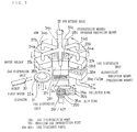
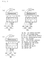
- Fig. 2, Figs. 3(a) to (c) and Fig. 4 are views for explaining a multistep process apparatus according to a second embodiment of the present invention, in which Fig. 2 is a perspective view of the whole apparatus, Figs. 3(a) to (c) show side views of the infrared radiation means, the ultraviolet radiation means and the gas dispersion unit, and Fig. 4 is a top view of the whole apparatus, respectively.
- Figs. 3(a) to (c) and Fig. 6 what distinguishes them from Figs. 1(a) and (b) is that the CVD reaction chamber and respective processing chambers are arranged along the circumference with the rotary shaft as the center, and a wafer holder having a heater (heating means) also moves along the circumference in accordance with the above.
- a wafer holder having a heater heating means
- Figs. 3(a) to (c) and Fig. 4, 37a to 37f shown in Figs. 3(a) to (c) represent wafer holders which are separated from one another, and respective wafer holders 37a to 37f are fixed to the rotary shaft 33 by means of arms 34a to 34f. Further, wafer setting surfaces 41a to 41f of the wafer holders 37a to 37f are rotated around the rotary shaft 33 on a plane including wafer setting surfaces 41a to 41f of respective wafer holders 37a to 37f by rotating the rotary shaft 33.
- respective wafer holders 37a to 37f are connected to an exhaust unit not illustrated, and fixed wafers 32a to 32f to the wafer setting surfaces 41a to 41f and/or separate the fixed wafers 32a to 32f from the wafer setting surfaces 41a to 41f by means of chucks which communicate with a suction port and an introduction port of nitrogen gas not illustrated through pipe-shaped arms 34a to 34f.
- heaters (heating means) 42a to 42f are buried in respective wafer holders 37a to 37f individually, and electric power is supplied independently to respective heaters 42a to 42f so that heating and thermal insulation of the wafers 32a to 32f placed on respective wafer holders 37a to 37f may be performed individually.
- 38b to 38f represent a gas dispersion unit of a first film forming section/infrared radiation means (processing means) of the first processing section/a gas dispersion unit of a second film forming section/ ultraviolet radiation means (processing means) of the second processing section/a gas dispersion unit of the third film forming section which are provided so as to oppose to the wafer setting surfaces 41b to 41f of the wafer holders 37b to 37f.
- 38b to 38f are separated from the wafer holders 37b to 37f and fixed to a base of an apparatus not illustrated along the circumstance with the rotary shaft 33 as the center.
- Respective gas dispersion units 38b, 38d and 38f have gas showers 43b, 43d and 43f for supplying the reaction gas to the wafers 32b, 32d and 32f and gas collectors 45b, 45d and 45f for collecting the gas in which reaction is completed, and reaction gas introduction ports 39b, 39d and 39f are connected to the gas showers 43b, 43d and 43f, and the gas discharge ports 40b, 40d and 40f are connected to the gas collectors 45b, 45d and 45f as shown typically by the gas dispersion unit 38f shown in Fig. 3(c). Furthermore, as shown in Fig. 4, the gas discharge sections of respective gas dispersion units 38b, 38d and 38f are provided by being split into a plurality of slits in a direction perpendicular to the radial direction with the rotary shaft 33 as the center.
- infrared radiation means 38c includes an infrared ray lamp 47c for heating the wafer 32c, an infrared ray lamp holder 46c for holding the infrared ray lamp 47c, and a gas collector 45c for collecting inert gas discharged onto the wafer for preventing oxidation, and a gas introduction port 39c is connected to the infrared ray lamp holder 46c and a gas discharge port 40c is connected to a gas collector 45c. Furthermore, as shown in Fig.
- ultraviolet radiation means 38e includes mercury lamps 49e for heating the wafer 32e, a mercury lamp holder 48e for holding the mercury lamps 49e and a gas collector 45e for collecting inert gas discharged onto the wafer for preventing oxidation, and a gas introduction port 39e is connected to the mercury lamp holder 48e and a gas discharge port 40e is connected to the gas collector 45e.
- slip rings 35a and 35b shown in Fig. 2 connected to the heater 42a are connected to a pair of collector rings 36a and 36b which are in contact with the slip rings 35a and 35b provided on the rotary shaft 33 and rotating along with the rotary shaft 33 so as to correspond to positive and negative polarities thereof.
- the pair of collector rings 36a and 36b are connected to a power source not illustrated so that electric power may be supplied to the heaters 42a to 42f through the slip rings 35a and 35b.
- only the slip rings 35a and 35b connected to the heater 42a of one wafer holder 37a are illustrated In Fig. 2, but slip rings connected to the heaters 42b to 42f of other wafer holders 37b to 37f are also provided on the rotary shaft 33.
- rotary connectors are used for both slip rings 35a and 35b so that the rotation of the rotary shaft 33 is not prevented.
- the position of the wafer holder 37a is a loader/unloader section where an elevator 31 is installed as shown in Fig. 2, and the wafer 32a is delivered between the elevator 31 and the wafer holder 37a only, and no film is formed.
- a multistep process apparatus of the second embodiment as described above, it becomes possible to form different types of multilayer films by providing the gas dispersion units 38b, 38d and 38f in plural numbers and separately from one another. Further, the infrared radiation means 38c and the ultraviolet radiation means 38e being provided, it is possible to perform formation of a flat insulating film, processing for flattening a formed film and processing for improvement of the film quality of a formed film continuously.
- the infrared radiation means 38c and the ultraviolet radiation means 38e are provided as processing means, but means for supplying processing gas such as ozone may be provided in place of these means, and furthermore, it is possible to increase the processing sections and to provide processing gas supplying means in addition to the infrared radiation means 38c and the ultraviolet radiation means 38e.
- the film forming section and the processing section are provided in a mixed state, but only the film forming section may be provided alone.
- wafer setting surfaces 41a to 41f with the faces thereof downward are provided, but the same is also applicable to that which has the wafer setting surfaces with the faces thereof upward.
- a manufacturing method according to a third embodiment in which a flattened BPSG film is formed on a wafer surface using a multistep process apparatus shown in Figs. 1(a) and (b) will be described with reference to Figs. 5(a) to (c) and Fig. 6.
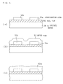
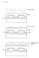
- Figs. 5(a) to (c) show sectional views for explaining a manufacturing method and
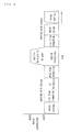
- Fig. 6 is a diagram showing hysteresis of the wafer temperature during film formation processing including the wafer temperature during movement.
- a Si substrate (wafer) 29 shown in Fig. 5(a) on which interconnection layers 51a and 51b composed of a polysilicon film are formed on a SiO 2 film 50 is placed with the face thereof downward on the wafer setting surface 13 of the wafer holder 15 after carrying the Si substrate 29 in the load/unload chamber 10 by the robot 16 shown in Fig. 1(b).
- the wafer holder 15 is moved so as to carry the wafer 29 to the CVD reaction chamber 11.
- electric current is also applied to the heater 14 during conveyance, thereby to run the heater 14 hot so that the wafer temperature is maintained at 400°C.
- mixed gas of TEOS/Tri-Methyl-Phosphate (TMP) containing phosphorus at 3.5 weight percentage/Tri-Methyl-Borate (TMB) containing boron at 4.0 weight percentage/O 3 is introduced into the gas shower 17 from the reaction gas introduction port 19, the mixed gas is discharged from the outgassing surface 18 onto the surface of the wafer 29. Therefore, when such a state is maintained for a predetermined period of time, a BPSG film 52 having a predetermined film thickness is formed (Fig. 5(b)).
- the wafer holder 15 is moved to the infrared heat processing chamber 12.
- electric current is also applied to the heater 14 during conveyance of the wafer similarly to the time of movement described above, thereby to run the heater 14 hot so that the wafer temperature is maintained at 400°C.
- the wafer 29 carried into the infrared heat processing chamber 12 is heated further by an infrared ray lamp 24 in nitrogen gas introduced through a gas introduction port 25 and is maintained at the temperature (the second temperature) of 800°C.
- the BPSG film 52 melts and flows, and the surface of the wafer 29 is flattened (Fig. 5(c)).
- the heat processing temperature could be lowered by approximately 100 to 200°C as compared with a conventional method for performing heat processing again in a heat processing furnace after the wafer is cooled naturally because the wafer is transferred from the CVD apparatus to the heat processing furnace. This is conceivable to be by reason of that, since the temperature of the wafer 29 is maintained at a predetermined temperature or higher, it is possible to prevent the film quality of the BPSG film 52 from changing and to prevent moisture absorption of the BPSG film 52.
- the wafer 29 held by the wafer holder 15 having the heater 14 is heated by means of the heater 14 and is maintained at the temperature of 400°C so as to form the BPSG film 52 on the surface of the wafer 29. Thereafter, the wafer 29 is heated by infrared radiation in addition to heating by the heater so as to rise the temperature of the wafer 29 from approximately 400°C to approximately 800°C for performing reflow processing of the BPSG film 52.
- the variation of the temperature of the wafer 29 can be reduced. With this, it is possible to aim at flattening of the BPSG film 52 and to prevent generation of thermal distortion in the BPSG film 52, thus preventing change and deterioration of the film quality of the BPSG film 52.
- reflow processing of the BPSG film 52 is performed after forming the BPSG film 52, but it is also possible to convey the wafer 29 while continuing heating of the wafer 29 after forming the BPSG film 52, and to perform UV radiation processing and annealing processing in an ozone atmosphere of the BPSG film 52 continuously on the wafer 29 maintained at a constant temperature.
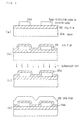
- Figs. 7(a) to (d) and Figs. 8(e) to (g) are sectional views for explaining the manufacturing method
- Fig. 9 is a diagram showing the hysteresis of the wafer temperature during film formation processing including the temperature of the wafer during movement.
- an insulating film having a three-layer construction of SiO 2 film 55a/BPSG film 56a/SiO 2 film 57 having a predetermined film thickness is formed on the wafer while the wafer holder 37a goes round the rotary shaft 33.
- the SiO 2 film 55a in the lowest layer is formed for the purpose of preventing a resistance value from fluctuating by the introduction of boron (B) and phosphorus (P) in the BPSG film 56a into polysilicon layers or silicide layers 54a and 54b, and the SiO 2 film 57 in the uppermost layer is formed for the purpose of preventing moisture absorption of the BPSG film 56a.
- a first wafer 32a on which polysilicon layers or silicide layers 54a and 54b are formed on a SiO 2 film 53 shown in Fig. 7(a) is conveyed to the loader/ unloader section and placed on the elevator 31 by means of a robot 30 shown in Fig. 2.
- the elevator 31 is lifted so as to bring the first wafer 32a into contact with a wafer setting surface 41a of the wafer holder 37a, and air is exhausted through a suction port not illustrated so as to place and fix the first wafer 32a onto the wafer setting surface 41a by means of a chuck communicating with the suction port.
- electric power is supplied to heaters 42a to 42f of all the wafer holders 37a to 37f through slip rings 35a, 35b, .../collector rings 36a, 36b, ... corresponding to heaters 42a to 42f of respective wafer holders 37a to 37f, and the temperature of the wafer setting surfaces 41a to 41f of all the wafer holders 37a to 37f is maintained at approximately 400°C.
- the rotary shaft 33 is rotated and the wafer holder 37a is stopped at a position right above a gas dispersion unit 38f. Then, the mixed gas of TEOS-O 3 is discharged from the gas shower 43f as reaction gas. At this time, a SiO 2 film 55 starts to grow, but the growth rate reaches to approximately 200 nm (2,000 ⁇ ).
- the SiO 2 film 55 having a target film thickness of approximately 200 nm (2,000 ⁇ ) is formed on the first wafer 32a (Fig. 7(b)) by maintaining such a state for about one minute.
- a second wafer 32b is placed on the wafer holder 37b positioned at the loader/unloader section similarly to the above, and the second wafer 32b is heated beforehand to reach the temperature at approximately 400°C by means of the heater 42b.
- the rotary shaft 33 is rotated, and the wafer holders 37b and 37a are stopped at positions right above the gas dispersion unit 38f/the ultraviolet radiation means 38e, respectively.
- the first and the second wafers 32a and 32b are also heated by means of the heaters 42a and 42b during movement so that the first and the second wafers 32a and 32b are maintained beforehand at the temperature of approximately 400°C as shown in Fig. 9.
- a mercury lamp 49e of the ultraviolet radiation means 38e is lighted so as to radiate ultraviolet rays onto the SiO 2 film 55 on the first wafer 32a.
- the mixed gas of TEOS-O 3 is discharged from the gas shower 43f as reaction gas, and, when this state is maintained for about one minute, a SiO 2 film having a target film thickness of approximately 200 nm (2,000 ⁇ ) is formed on the second wafer 32b. Furthermore, in the interim, a third wafer 32c is placed on the wafer holder 37c positioned at the loader/unloader section similarly to the above, and the third wafer 32c is heated beforehand to the temperature of approximately 400°C by means of the heater 42c.
- the rotary shaft 33 is rotated, and the wafer holders 37c, 37b and 37a are stopped at positions right above the gas dispersion unit 38f/the ultraviolet radiation means 38e/the gas dispersion unit 38d, respectively.
- the first, the second and the third wafers 32a, 32b and 32c are also heated by the heaters 42a to 42c during movement so as to maintain the first, the second and the third wafers at the temperature of approximately 400°C as shown in Fig. 9.
- a SiO 2 film having a target film thickness of approximately 200 nm (2,000 ⁇ ) is formed on the third wafer 32c by discharging reaction gas from the gas dispersion unit 38f.
- a fourth wafer 32d is placed on the wafer holder 37d positioned at the loader/unloader section similarly to the above, and the fourth wafer 32d is heated to the temperature of approximately 400°C by means of the heater 42d.
- the rotary shaft 33 is rotated, and the wafer holders 37d, 37c, 37b and 37a are stopped at positions right above the gas dispersion unit 38f/the ultraviolet radiation means 38e/the gas dispersion unit 38d/the infrared radiation means 38c, respectively.
- the first, the second, the third and the fourth wafers 32a, 32b, 32c and 32d are also heated during movement by means of the heaters 42a to 42d, and the first, the second, the third and the fourth wafers 32a, 32b, 32c and 32d are maintained beforehand at the temperature of approximately 400°C as shown in Fig. 9.
- an infrared ray lamp 38c is lighted, and the wafer temperature is risen from approximately 400°C to approximately 800°C and maintained there as shown in Fig. 9.
- the BPSG film 56 melts and flows, and the unevenness of the wafer surface is levelled (Fig. 7(e)).
- predetermined processings are performed also on the second, the third and the fourth wafers 32b, 32c and 32d simultaneously with the processing of the first wafer 32a.
- a fifth wafer 32e is placed on the wafer holder 37e positioned at the loader/unloader section similarly to the above, and the fourth wafer 32e is heated to the temperature of approximately 400°C beforehand by means of the heater 42e.
- the rotary shaft 33 is rotated, and the wafer holders 37e, 37d, 37c, 37b and 37a are stopped at positions right above the gas dispersion unit 38f/the ultraviolet radiation means 38e/the gas dispersion unit 38d/the infrared radiation means 38c/the gas dispersion unit 38b, respectively.
- the first, the second, the third, the fourth and the fifth wafers 32a, 32b, 32c, 32d and 32e are also heated during movement by means of the heaters 42a to 42e so as to maintain the first, the second, the third, the fourth and the fifth wafers 32a, 32b, 32c, 32d and 32e at the temperature of approximately 400°C beforehand.
- the mixed gas of TEOS-O 3 is discharged from the gas shower 43b of the gas dispersion unit 38b as reaction gas, and when this state is maintained for about one minute, a SiO 2 film 57 having a target film thickness of approximately 200 nm (2,000 ⁇ ) is formed on the first wafer 32a (Fig. 7(f)).
- predetermined processings are applied also to the second, the third, the fourth and the fifth wafers 32b, 32c, 32d and 32e simultaneously with the processing of the first wafer 32a.
- a sixth wafer 32f is placed on the wafer holder 37f positioned at the loader/unloader section similarly to the above, and the sixth wafer 32f is heated beforehand to the temperature of approximately 400°C by means of the heater 42f.
- the rotary shaft 33 is rotated, and the wafer holders 37f, 37e, 37d, 37c, 37b and 37a are stopped at positions right above the gas dispersion unit 38f/the ultraviolet radiation means 38e/the gas dispersion unit 38d/the infrared radiation means 38c/the gas dispersion unit 38b/the elevator 31, respectively.
- the suction port corresponding to the chuck of the wafer holder 37a is closed, and the valve at the introduction port of nitrogen gas is opened so as to supply the nitrogen gas to the chuck, the first wafer 32a is separated from the wafer setting surfaces 41a and is placed on the elevator 31.
- the first wafer 32a is carried out to the cassette station by means of the robot 30.
- predetermined processings are also applied to the second, the third, the fourth, the fifth and the sixth wafers 32b, 32c, 32d, 32e and 32f simultaneously with the processing of the first wafer 32a.
- the first, the second, the third, the fourth, the fifth and the sixth wafers 32a, 32b, 32c, 32d, 32e and 32f held by the wafer holders 37a, 37b, 37c, 37d, 37e and 37f having heaters 42a to 42f are moved between the gas dispersion units 38b, 38d and 38f and respective processing sections 38c and 38e while heating these wafers and maintaining them at the temperature of approximately 400°C, thereby to form SiO 2 film 55a radiated with ultraviolet rays/BPSG film 56a flattened by infrared radiation/SiO 2 film 57 on the surfaces of the wafers 32a, 32b, 32c, 32d, 32e and 32f.
- the wafer temperature only fluctuates between 400°C and 800°C as shown in Fig. 9. Since it is possible to reduce the variation of the wafer temperature by preventing the wafers 32a, 32b, 32c, 32d, 32e and 32f from being cooled naturally during movement as in the past, it is possible to prevent change and deterioration of the film quality of the formed film in such a manner that thermal distortion is reduced and so on.
- the SiO 2 film 55a radiated with ultraviolet rays is formed as a SiO 2 film in a lowermost layer in the fourth embodiment, but it is also possible to form a SiO 2 film applied with annealing processing in an ozone atmosphere. Further, it is possible to form not only a film having the film thickness in the fourth embodiment, but also to form a film having another constructions by combining film formation, infrared processing, ultraviolet processing, annealing processing in an ozone atmosphere and the like.
- film formation and processing of a formed film are performed, but it is also possible to form a film composed of different types of multilayers of SiO 2 film/BPSG film/SiO 2 film without processing a formed film. In this case, it is also possible to reduce variation of the wafer temperature by heating the wafer while the wafer holder is moved among film forming sections. Thus, it is possible to aim at reduction of thermal distortion of the formed insulating film.
- an apparatus for manufacturing a semiconductor device and a method for manufacturing a semiconductor device according to the present invention are useful as an apparatus for manufacturing a semiconductor device and a method for manufacturing a semiconductor device such as what is called a multistep process apparatus which is capable of forming a film in a single layer having an improved film quality by performing different types of processings continuously without having the wafers get out in the air.
- mercury lamp 50, 53, 55, 55a, 57 ... SiO 2 films; 51a, 51b, 58 ... interconnection layers; 52, 52a, 56, 56a ... BPSG films; 54a, 54b ... polysilicon layers or silicide layers.
Landscapes
- Chemical & Material Sciences (AREA)
- General Chemical & Material Sciences (AREA)
- Chemical Kinetics & Catalysis (AREA)
- Engineering & Computer Science (AREA)
- Materials Engineering (AREA)
- Mechanical Engineering (AREA)
- Metallurgy (AREA)
- Organic Chemistry (AREA)
- Health & Medical Sciences (AREA)
- Toxicology (AREA)
- Formation Of Insulating Films (AREA)
- Container, Conveyance, Adherence, Positioning, Of Wafer (AREA)
- Internal Circuitry In Semiconductor Integrated Circuit Devices (AREA)
Abstract
Description
- The present invention relates to an apparatus for manufacturing a semiconductor device and a method for manufacturing a semiconductor device such as what is called a multistep process apparatus which is capable of forming a single layer film and a multilayer film having improved film quality by performing different types of processings continuously without having a wafer get out in the air.
- In an apparatus for manufacturing a very large integrate circuit (VLSI) semiconductor device, the apparatus that incorporates a conception of a multiprocess in which several processings are performed continuously without having the semiconductor device get out in the air has become the main current in recent years, thus making it possible to aim at improvement of the film quality of a formed film and the like and improvement of adhesion among multiple layers of the film. As the combination of processings, for example, film formation and etch back after film formation, processing before oxidation and formation of an oxide film, and continuous formation of a barrier metal film/a metal film may be mentioned.
- As representative apparatus for manufacturing a semiconductor device capable of such processing, there are what is called a multi-chamber process apparatus using multi-chambers, a multistep process apparatus or a cluster apparatus in which respective processing sections are arranged in close vicinity to one another and the like.
- Fig. 10 is a block diagram showing an apparatus for manufacturing a semiconductor device in which an insulating film is formed on a wafer by performing different types of processings continuously using conventional multi-chambers.
- In Fig. 10, a
reference numeral 1 represents a cassette chamber for preparing for carrying a wafer into and out of the multi-chambers, 3 represents a load-lock chamber for adjusting the pressure among chambers in carrying-in and carrying-out of the wafer, 7a represents a valve for opening and closing a part between thecassette chamber 1 and the load-lock chamber robot 5 for carrying the wafer is installed, 7b is a valve for opening and closing a part between the load-lock chamber 3 and thebuffer chamber buffer chamber 4 as the center. They are used for the purposes described hereunder. For example: - (1) the
processing chamber 6a is used for forming a SiO2 film (film formation temperature at 400°C) by a plasma chemical vapor deposition (CVD) method; - (2) the
processing chamber 6b is used for forming a PSG film (film formation temperature at 400°C) by a low pressure CVD method; - (3) the
processing chamber 6c is used for etching back (at room temperature) of a formed film; - (4) the
processing chamber 6d is used for forming a Si3N4 film (film formation temperature at 400°C) by a plasma CVD method; and - (5) the
processing chamber 6e is used for forming a SiO2 film (film formation temperature at 400°C) by a low pressure CVD method. Besides, heaters not illustrated for maintaining awafer 9 at the film formation temperature are provided inrespective processing chambers 6a to 6e. Further, 8a to 8e represent valves for opening and closing the parts between thebuffer chamber 4 andrespective processing chambers 6a to 6e. In addition, 2 represents a robot for delivering thewafer 9 from thecassette chamber 1 to a robot not illustrated provided in the load-lock chamber 3. -
- When a flat multi-layer insulating film composed of SiO2 film/PSG film is formed using the above-described apparatus for manufacturing a semiconductor device, the
wafer 9 moves among the chambers as described hereunder. Namely, therobot 5 carries thewafer 9 into and out ofrespective processing chambers processing chamber 6a/theprocessing chamber 6b/theprocessing chamber 6c. - Now, the heaters for heating and maintaining the
wafer 9 at the film formation temperature are provided inrespective processing chambers wafer 9 varies between the room temperature and the film formation temperature while thewafer 9 moves among theprocessing chambers wafer 9 is subject to a certain type of temperature cycle, degradation and deterioration of the film quality of the formed CVD film or generation of a stress to the formed film and the like are caused. - Further, in a process requiring annealing after forming a CVD film, the wafer is taken out and housed in a cassette once after forming a CVD film, and the cassette is moved and inserted into a heating furnace, thereafter so as to apply heat processing. Temperature hysteresis of a wafer in such a case is shown in Fig. 11.
- In this case, there is also a problem that the wafer temperature varies more sharply than a conventional example shown in Fig. 10 from the room temperature to 1,000°C.
- From EP-A-0 532 758, a semiconductor manufacturing equipment is known, which has only a film forming gas dispersion unit but does not comprise processing means for processing a formed film, such as ultraviolet ray radiation means or infrared ray radiation means.
- JP-A-3-54844 discloses transporting means provided with heating means and a plurality of processing portions provided each with another heating means. The transporting means carry a wafer to each processing portion and then transfers it thereto. The wafer is heated separately by the heating means of each processing portion during processing.
- It is an object of the present invention which has been made in view of such conventional problems to provide an apparatus for manufacturing a semiconductor device and a method for manufacturing a semiconductor device that are capable of preventing thermal distortion and the like from generating and also preventing variation and deterioration of the film quality of the formed film by reducing the variation of the wafer temperature while different types of processings are performed successively.
- The above object is attained by an apparatus according to
claim 1 and methods according toclaims subclaim 2 defines an advantageous embodiment of the invention. - In case of performing, after forming a film in the film forming section, other processings at other locations, i.e., in case of performing reflow processing of a film, processing by radiating ultraviolet rays (UV), or anneal processing in a ozone gas atmosphere in the processing section by means for radiating infrared rays, means for radiating ultraviolet rays or means for supplying ozone gas, it is possible to reduce temperature variation of the wafer by preventing natural cooling of the wafer during movement by heating the wafer with the heating means in all cases.
- When different types of plurality of films are formed on the wafer, it is possible to maintain the wafer temperature at the forming temperature of one film for instance during the period of moving the wafer for forming other films after forming the one film. Thus, it is possible to reduce variation of the wafer temperature by preventing natural cooling during the movement of the wafer and to prevent change and deterioration of the film quality of the formed film by preventing generation of thermal distortion and the like in the formed film.
- It is possible to perform processing continuously without lowering the wafer temperature as being done in the past. Thus, it is possible to reduce variation of the wafer temperature. As a result, it is possible to prevent generation of thermal distortion in the formed film, thereby to prevent change and deterioration of the film quality of the formed film.
-
- Fig. 1 is a block diagram for explaining a multistep process apparatus showing a first embodiment of the present invention;
- Fig. 2 is a perspective view for explaining a multistep process apparatus showing a second embodiment of the present invention;
- Fig. 3 shows block diagrams for explaining a film forming section and a processing section of a multistep process apparatus according to the second embodiment of the present invention;
- Fig. 4 is a top view for explaining a multistep process apparatus according to the second embodiment of the present invention;
- Fig. 5 shows sectional views for explaining a method for forming a film according to a third embodiment of the present invention;
- Fig. 6 is a diagram for explaining hysteresis of the wafer temperature in a method for forming a film according to the third embodiment of the present invention;
- Fig. 7 shows sectional views (1/2) for explaining a method for forming a film according to a fourth embodiment of the present invention;
- Fig. 8 shows sectional views (2/2) for explaining a method for forming a film according to the fourth embodiment of the present invention;
- Fig. 9 is a diagram for explaining hysteresis of the wafer temperature in a method for forming a film according to the fourth embodiment of the present invention;
- Fig. 10 is a block diagram for explaining a conventional multi-chamber process apparatus; and
- Fig. 11 is a diagram for explaining hysteresis of the wafer temperature in a conventional method for forming a film.
-
- Embodiments of the present invention will be described hereinafter with reference to the drawings.
- Figs. 1(a) and (b) show what is called a multi step process apparatus of the first embodiment of the present invention, in which Fig. 1(a) is a plan view and Fig. 1(b) is a side view.
- In a multistep process apparatus shown in Figs. 1(a) and (b), a load/
unload chamber 10, a CVD reaction chamber (a film forming section) 11 and an infrared heat processing chamber (a processing section) 12 are connected in this arrangement, a BPSG film is formed by a CVD method on a wafer surface held with the face downward in order to prevent contamination due to dust and the like, and reflow processing is performed further, thereby making it possible to flatten the wafer surface. Besides, valves for opening and closing partition walls among respective chambers and the portions among respective chambers are provided sometimes. - A
reference numeral 16 in the figure represents a robot provided in the load/unload chamber 10, and carries in and carries out awafer 29 from the outside of the load/unload chamber 10. - 22 represents a gas dispersion unit provided in the
CVD reaction chamber 11, which introduces reaction gas through a reactiongas introduction port 19 and discharges reaction gas upwards from an outgassing surface of agas shower 17. Then, the reaction gas which has completed reaction is collected by agas collector 20 surrounding the peripheral part of thegas shower 17 and exhausted outside theCVD reaction chamber 11 through agas discharge port 21. - 28 represents infrared radiation means (processing means) provided in the infrared heat processing chamber 12, and an
infrared ray lamps 24 are held by an infraredray lamp holder 23 having agas introduction port 25 for introducing inert gas discharged onto thewafer 29 for preventing oxidation. The inert gas dispersed on the surface of thewafer 29 is collected by the gas collector provided around the infraredray lamp holder 23, and is discharged outside the infrared heat processing chamber 12 through agas exhaust port 27. - 15 represents a wafer holder for holding the
wafer 29 with the face downward for preventing contamination due to dust and the like, which comes and goes among the load/unload chamber 10, theCVD reaction chamber 11 and the infrared heat processing chamber 12 while holding thewafer 29 as it is. Further, a heater (heating means) 14 is buried in thewafer holder 15 so as to heat and maintain thewafer 29 placed on awafer setting surface 13 at a predetermined temperature. - As described above, in a multistep process apparatus of the first embodiment of the present invention, the
CVD reaction chamber 11 having thegas dispersion unit 22 for supplying the reaction gas onto thewafer 29, an infrared heat processing chamber 12 for heating and reflowing a film such as a formed BPSG film, and thewafer holder 15 capable of moving between theCVD reaction chamber 11 and the infrared heat processing chamber 12 successively while holding thewafer 29 as it is are provided, and thewafer holder 15 has theheater 14 capable of heating thewafer 29 including the period while thewafer 29 is moving. - Accordingly, when reflow processing of a BPSG film is performed by the infrared radiation means 28 in the infrared heat processing chamber 12 after a film such as a BPSG film is formed in the
CVD reaction chamber 11, it is possible to maintain the wafer temperature at a predetermined temperature by adjusting heating by means of theheater 14. Thus, it is possible to reduce the temperature variation of thewafer 29. - Besides, in the first embodiment, the infrared heat processing chamber 12 is connected to the
CVD reaction chamber 11, but a UV processing chamber (an ultraviolet processing chamber) or an ozone processing chamber may be connected in place of the infrared heat processing chamber 12. With this, it is possible to densify a film such as a BPSG film by filling with dangling bond, and also to prevent generation of thermal distortion in a formed film by reducing temperature variation of thewafer 29, thereby to aim at improvement of the film quality. - Fig. 2, Figs. 3(a) to (c) and Fig. 4 are views for explaining a multistep process apparatus according to a second embodiment of the present invention, in which Fig. 2 is a perspective view of the whole apparatus, Figs. 3(a) to (c) show side views of the infrared radiation means, the ultraviolet radiation means and the gas dispersion unit, and Fig. 4 is a top view of the whole apparatus, respectively.
- In Fig. 2, Figs. 3(a) to (c) and Fig. 6, what distinguishes them from Figs. 1(a) and (b) is that the CVD reaction chamber and respective processing chambers are arranged along the circumference with the rotary shaft as the center, and a wafer holder having a heater (heating means) also moves along the circumference in accordance with the above. In this multistep process apparatus, it is possible to form, for example, an insulating film having a 3-layer construction in which a BPSG film flattened by reflow is put between SiO2 films.
- In Fig. 2, Figs. 3(a) to (c) and Fig. 4, 37a to 37f shown in Figs. 3(a) to (c) represent wafer holders which are separated from one another, and
respective wafer holders 37a to 37f are fixed to therotary shaft 33 by means ofarms 34a to 34f. Further, wafer setting surfaces 41a to 41f of thewafer holders 37a to 37f are rotated around therotary shaft 33 on a plane including wafer setting surfaces 41a to 41f ofrespective wafer holders 37a to 37f by rotating therotary shaft 33. Also,respective wafer holders 37a to 37f are connected to an exhaust unit not illustrated, and fixedwafers 32a to 32f to the wafer setting surfaces 41a to 41f and/or separate the fixedwafers 32a to 32f from the wafer setting surfaces 41a to 41f by means of chucks which communicate with a suction port and an introduction port of nitrogen gas not illustrated through pipe-shapedarms 34a to 34f. Further, heaters (heating means) 42a to 42f are buried inrespective wafer holders 37a to 37f individually, and electric power is supplied independently to respective heaters 42a to 42f so that heating and thermal insulation of thewafers 32a to 32f placed onrespective wafer holders 37a to 37f may be performed individually. - 38b to 38f represent a gas dispersion unit of a first film forming section/infrared radiation means (processing means) of the first processing section/a gas dispersion unit of a second film forming section/ ultraviolet radiation means (processing means) of the second processing section/a gas dispersion unit of the third film forming section which are provided so as to oppose to the wafer setting surfaces 41b to 41f of the
wafer holders 37b to 37f. 38b to 38f are separated from thewafer holders 37b to 37f and fixed to a base of an apparatus not illustrated along the circumstance with therotary shaft 33 as the center. - Respective
gas dispersion units gas showers 43b, 43d and 43f for supplying the reaction gas to thewafers 32b, 32d and 32f and gas collectors 45b, 45d and 45f for collecting the gas in which reaction is completed, and reactiongas introduction ports 39b, 39d and 39f are connected to thegas showers 43b, 43d and 43f, and thegas discharge ports 40b, 40d and 40f are connected to the gas collectors 45b, 45d and 45f as shown typically by thegas dispersion unit 38f shown in Fig. 3(c). Furthermore, as shown in Fig. 4, the gas discharge sections of respectivegas dispersion units rotary shaft 33 as the center. - Further, as shown in Fig. 3(a), infrared radiation means 38c includes an
infrared ray lamp 47c for heating thewafer 32c, an infrared ray lamp holder 46c for holding theinfrared ray lamp 47c, and a gas collector 45c for collecting inert gas discharged onto the wafer for preventing oxidation, and agas introduction port 39c is connected to the infrared ray lamp holder 46c and agas discharge port 40c is connected to a gas collector 45c. Furthermore, as shown in Fig. 3(b), ultraviolet radiation means 38e includesmercury lamps 49e for heating thewafer 32e, amercury lamp holder 48e for holding themercury lamps 49e and agas collector 45e for collecting inert gas discharged onto the wafer for preventing oxidation, and agas introduction port 39e is connected to themercury lamp holder 48e and agas discharge port 40e is connected to thegas collector 45e. - Furthermore,
slip rings slip rings rotary shaft 33 and rotating along with therotary shaft 33 so as to correspond to positive and negative polarities thereof. Further, the pair of collector rings 36a and 36b are connected to a power source not illustrated so that electric power may be supplied to the heaters 42a to 42f through theslip rings slip rings wafer holder 37a are illustrated In Fig. 2, but slip rings connected to the heaters 42b to 42f ofother wafer holders 37b to 37f are also provided on therotary shaft 33. Further, rotary connectors are used for bothslip rings rotary shaft 33 is not prevented. - Besides, the position of the
wafer holder 37a is a loader/unloader section where anelevator 31 is installed as shown in Fig. 2, and thewafer 32a is delivered between theelevator 31 and thewafer holder 37a only, and no film is formed. - In a multistep process apparatus of the second embodiment as described above, it becomes possible to form different types of multilayer films by providing the
gas dispersion units - Besides, in the above-described second embodiment, the infrared radiation means 38c and the ultraviolet radiation means 38e are provided as processing means, but means for supplying processing gas such as ozone may be provided in place of these means, and furthermore, it is possible to increase the processing sections and to provide processing gas supplying means in addition to the infrared radiation means 38c and the ultraviolet radiation means 38e.
- Further, the film forming section and the processing section are provided in a mixed state, but only the film forming section may be provided alone.
- Furthermore, the wafer setting surfaces 41a to 41f with the faces thereof downward are provided, but the same is also applicable to that which has the wafer setting surfaces with the faces thereof upward.
- Next, a manufacturing method according to a third embodiment in which a flattened BPSG film is formed on a wafer surface using a multistep process apparatus shown in Figs. 1(a) and (b) will be described with reference to Figs. 5(a) to (c) and Fig. 6. Figs. 5(a) to (c) show sectional views for explaining a manufacturing method and Fig. 6 is a diagram showing hysteresis of the wafer temperature during film formation processing including the wafer temperature during movement.
- First, a Si substrate (wafer) 29 shown in Fig. 5(a) on which interconnection layers 51a and 51b composed of a polysilicon film are formed on a SiO2 film 50 is placed with the face thereof downward on the
wafer setting surface 13 of thewafer holder 15 after carrying theSi substrate 29 in the load/unloadchamber 10 by therobot 16 shown in Fig. 1(b). - Next, electric current is applied to the
heater 14 buried in thewafer holder 15 so as to run theheater 14 hot, thereby to heat thewafer 29 to maintain the wafer temperature (the first temperature)at 400°C. - Then, the
wafer holder 15 is moved so as to carry thewafer 29 to theCVD reaction chamber 11. At this time, electric current is also applied to theheater 14 during conveyance, thereby to run theheater 14 hot so that the wafer temperature is maintained at 400°C. Then, when mixed gas of TEOS/Tri-Methyl-Phosphate (TMP) containing phosphorus at 3.5 weight percentage/Tri-Methyl-Borate (TMB) containing boron at 4.0 weight percentage/O3 is introduced into thegas shower 17 from the reactiongas introduction port 19, the mixed gas is discharged from theoutgassing surface 18 onto the surface of thewafer 29. Therefore, when such a state is maintained for a predetermined period of time, aBPSG film 52 having a predetermined film thickness is formed (Fig. 5(b)). - Then, the
wafer holder 15 is moved to the infrared heat processing chamber 12. At this time, electric current is also applied to theheater 14 during conveyance of the wafer similarly to the time of movement described above, thereby to run theheater 14 hot so that the wafer temperature is maintained at 400°C. - Then, the
wafer 29 carried into the infrared heat processing chamber 12 is heated further by aninfrared ray lamp 24 in nitrogen gas introduced through agas introduction port 25 and is maintained at the temperature (the second temperature) of 800°C. As a result, theBPSG film 52 melts and flows, and the surface of thewafer 29 is flattened (Fig. 5(c)). At this time, the heat processing temperature could be lowered by approximately 100 to 200°C as compared with a conventional method for performing heat processing again in a heat processing furnace after the wafer is cooled naturally because the wafer is transferred from the CVD apparatus to the heat processing furnace. This is conceivable to be by reason of that, since the temperature of thewafer 29 is maintained at a predetermined temperature or higher, it is possible to prevent the film quality of theBPSG film 52 from changing and to prevent moisture absorption of theBPSG film 52. - As described above, in the manufacturing method of the third embodiment, as shown in the hysteresis of the wafer temperature shown in Fig. 6, the
wafer 29 held by thewafer holder 15 having theheater 14 is heated by means of theheater 14 and is maintained at the temperature of 400°C so as to form theBPSG film 52 on the surface of thewafer 29. Thereafter, thewafer 29 is heated by infrared radiation in addition to heating by the heater so as to rise the temperature of thewafer 29 from approximately 400°C to approximately 800°C for performing reflow processing of theBPSG film 52. - Accordingly, since it is possible to perform reflow processing of the
BPSG film 52 continuously after theBPSG film 52 is formed without lowering the temperature of thewafer 29, the variation of the temperature of thewafer 29 can be reduced. With this, it is possible to aim at flattening of theBPSG film 52 and to prevent generation of thermal distortion in theBPSG film 52, thus preventing change and deterioration of the film quality of theBPSG film 52. - Further, reflow processing of the
BPSG film 52 is performed after forming theBPSG film 52, but it is also possible to convey thewafer 29 while continuing heating of thewafer 29 after forming theBPSG film 52, and to perform UV radiation processing and annealing processing in an ozone atmosphere of theBPSG film 52 continuously on thewafer 29 maintained at a constant temperature. With this, it is possible to densify theBPSG film 52 by filling dangling bond, and also to reduce temperature variation of thewafer 29 between the time of processing and the time of conveyance so as to prevent generation of thermal distortion in theBPSG film 52, thus aiming at improvement of the film quality. - Next, a method for forming an insulating film in three layers according to a fourth embodiment of the present invention using the multistep process apparatus shown in Fig. 2 will be described with reference to Figs. 7(a) to (d), Figs. 8(e) to (g) and Fig. 9.
- Figs. 7(a) to (d) and Figs. 8(e) to (g) are sectional views for explaining the manufacturing method, and Fig. 9 is a diagram showing the hysteresis of the wafer temperature during film formation processing including the temperature of the wafer during movement. In this case, as shown in Fig. 8(f), an insulating film having a three-layer construction of SiO2 film 55a/
BPSG film 56a/SiO2 film 57 having a predetermined film thickness is formed on the wafer while thewafer holder 37a goes round therotary shaft 33. Besides, the SiO2 film 55a in the lowest layer is formed for the purpose of preventing a resistance value from fluctuating by the introduction of boron (B) and phosphorus (P) in theBPSG film 56a into polysilicon layers orsilicide layers BPSG film 56a. - First, a
first wafer 32a on which polysilicon layers orsilicide layers elevator 31 by means of arobot 30 shown in Fig. 2. - Then, the
elevator 31 is lifted so as to bring thefirst wafer 32a into contact with a wafer setting surface 41a of thewafer holder 37a, and air is exhausted through a suction port not illustrated so as to place and fix thefirst wafer 32a onto the wafer setting surface 41a by means of a chuck communicating with the suction port. At this time, electric power is supplied to heaters 42a to 42f of all thewafer holders 37a to 37f throughslip rings respective wafer holders 37a to 37f, and the temperature of the wafer setting surfaces 41a to 41f of all thewafer holders 37a to 37f is maintained at approximately 400°C. - Next, after the temperature of the
first wafer 32a reaches to approximately 400°C, therotary shaft 33 is rotated and thewafer holder 37a is stopped at a position right above agas dispersion unit 38f. Then, the mixed gas of TEOS-O3 is discharged from thegas shower 43f as reaction gas. At this time, a SiO2 film 55 starts to grow, but the growth rate reaches to approximately 200 nm (2,000Å). The SiO2 film 55 having a target film thickness of approximately 200 nm (2,000Å) is formed on thefirst wafer 32a (Fig. 7(b)) by maintaining such a state for about one minute. Besides, in the interim, a second wafer 32b is placed on thewafer holder 37b positioned at the loader/unloader section similarly to the above, and the second wafer 32b is heated beforehand to reach the temperature at approximately 400°C by means of the heater 42b. - Next, the
rotary shaft 33 is rotated, and thewafer holders gas dispersion unit 38f/the ultraviolet radiation means 38e, respectively. At this time, the first and thesecond wafers 32a and 32b are also heated by means of the heaters 42a and 42b during movement so that the first and thesecond wafers 32a and 32b are maintained beforehand at the temperature of approximately 400°C as shown in Fig. 9. In this state, amercury lamp 49e of the ultraviolet radiation means 38e is lighted so as to radiate ultraviolet rays onto the SiO2 film 55 on thefirst wafer 32a. As a result, it is possible to fill dangling bond of the SiO2 film 55 so as to densify the SiO2 film 55a (Fig. 7(c)). On the other hand, the mixed gas of TEOS-O3 is discharged from thegas shower 43f as reaction gas, and, when this state is maintained for about one minute, a SiO2 film having a target film thickness of approximately 200 nm (2,000Å) is formed on the second wafer 32b. Furthermore, in the interim, athird wafer 32c is placed on thewafer holder 37c positioned at the loader/unloader section similarly to the above, and thethird wafer 32c is heated beforehand to the temperature of approximately 400°C by means of theheater 42c. - Then, the
rotary shaft 33 is rotated, and thewafer holders gas dispersion unit 38f/the ultraviolet radiation means 38e/thegas dispersion unit 38d, respectively. At this time, the first, the second and thethird wafers gas dispersion unit 38d as reaction gas, and, when this state is maintained for about three minutes, aBPSG film 56 having a target film thickness of approximately 600 nm (6,000Å) is formed on the SiO2 film 55 of thefirst wafer 32a (Fig. 7(d)). On the other hand, themercury lamp 49e is lighted so as to radiate ultraviolet rays onto the SiO2 film on the second wafer 32b. As a result, it is possible to fill dangling bond of the SiO2 film so as to densify the SiO2 film. Furthermore, a SiO2 film having a target film thickness of approximately 200 nm (2,000Å) is formed on thethird wafer 32c by discharging reaction gas from thegas dispersion unit 38f. Moreover, in the interim, a fourth wafer 32d is placed on thewafer holder 37d positioned at the loader/unloader section similarly to the above, and the fourth wafer 32d is heated to the temperature of approximately 400°C by means of the heater 42d. - Next, the
rotary shaft 33 is rotated, and thewafer holders gas dispersion unit 38f/the ultraviolet radiation means 38e/thegas dispersion unit 38d/the infrared radiation means 38c, respectively. At this time, the first, the second, the third and thefourth wafers fourth wafers BPSG film 56 on thefirst wafer 32a, aninfrared ray lamp 38c is lighted, and the wafer temperature is risen from approximately 400°C to approximately 800°C and maintained there as shown in Fig. 9. When this state is maintained for a predetermined period of time, theBPSG film 56 melts and flows, and the unevenness of the wafer surface is levelled (Fig. 7(e)). Besides, predetermined processings are performed also on the second, the third and thefourth wafers 32b, 32c and 32d simultaneously with the processing of thefirst wafer 32a. Furthermore, in the interim, afifth wafer 32e is placed on thewafer holder 37e positioned at the loader/unloader section similarly to the above, and thefourth wafer 32e is heated to the temperature of approximately 400°C beforehand by means of theheater 42e. - Then, the
rotary shaft 33 is rotated, and thewafer holders gas dispersion unit 38f/the ultraviolet radiation means 38e/thegas dispersion unit 38d/the infrared radiation means 38c/thegas dispersion unit 38b, respectively. At this time, the first, the second, the third, the fourth and thefifth wafers fifth wafers gas dispersion unit 38b as reaction gas, and when this state is maintained for about one minute, a SiO2 film 57 having a target film thickness of approximately 200 nm (2,000Å) is formed on thefirst wafer 32a (Fig. 7(f)). Besides, predetermined processings are applied also to the second, the third, the fourth and thefifth wafers first wafer 32a. Furthermore, in the interim, asixth wafer 32f is placed on thewafer holder 37f positioned at the loader/unloader section similarly to the above, and thesixth wafer 32f is heated beforehand to the temperature of approximately 400°C by means of theheater 42f. - Then, the
rotary shaft 33 is rotated, and thewafer holders gas dispersion unit 38f/the ultraviolet radiation means 38e/thegas dispersion unit 38d/the infrared radiation means 38c/thegas dispersion unit 38b/theelevator 31, respectively. Then, when theelevator 31 is lifted, the suction port corresponding to the chuck of thewafer holder 37a is closed, and the valve at the introduction port of nitrogen gas is opened so as to supply the nitrogen gas to the chuck, thefirst wafer 32a is separated from the wafer setting surfaces 41a and is placed on theelevator 31. Next, thefirst wafer 32a is carried out to the cassette station by means of therobot 30. Besides, in the interim, predetermined processings are also applied to the second, the third, the fourth, the fifth and thesixth wafers first wafer 32a. - In such a manner, similar processing to that for the
first wafer 32a is also performed to the second, the third, the fourth, the fifth and thesixth wafers fifth wafers rotary shaft 33, a film in three layers of SiO2 film/BPSG film/SiO2,film having a target film thickness has been formed on these wafers. The wafers are heated by means of the heaters 42b to 42e in the interim, and always maintained at a constant temperature. Therefore, it is possible to prevent generation of thermal distortion on the formed film due to temperature variation. In such a way, a film in three layers of SiO2 film/BPSG film/SiO2 film each having a predetermined film thickness is formed on the wafer one after another and accumulated in the cassette station. - When an
interconnection layer 58 in an upper layer composed of an Aℓ film is formed thereafter after a via hole not illustrated is formed in the SiO2 film 57 and aBPSG film 56a oninterconnection layers - As described above, according to the method for manufacturing a semiconductor device of the fourth embodiment, the first, the second, the third, the fourth, the fifth and the
sixth wafers wafer holders gas dispersion units respective processing sections BPSG film 56a flattened by infrared radiation/SiO2 film 57 on the surfaces of thewafers - Accordingly, the wafer temperature only fluctuates between 400°C and 800°C as shown in Fig. 9. Since it is possible to reduce the variation of the wafer temperature by preventing the
wafers - Besides, the SiO2 film 55a radiated with ultraviolet rays is formed as a SiO2 film in a lowermost layer in the fourth embodiment, but it is also possible to form a SiO2 film applied with annealing processing in an ozone atmosphere. Further, it is possible to form not only a film having the film thickness in the fourth embodiment, but also to form a film having another constructions by combining film formation, infrared processing, ultraviolet processing, annealing processing in an ozone atmosphere and the like.
- Further, film formation and processing of a formed film are performed, but it is also possible to form a film composed of different types of multilayers of SiO2 film/BPSG film/SiO2 film without processing a formed film. In this case, it is also possible to reduce variation of the wafer temperature by heating the wafer while the wafer holder is moved among film forming sections. Thus, it is possible to aim at reduction of thermal distortion of the formed insulating film.
- Furthermore, it is possible to unify supply of reaction gas onto the
wafers 32a to 32f thereby to form SiO2 film/BPSG film/SiO2 film each having uniform film thickness and film quality by having thewafer holders 37a to 37f perform rectilinear reciprocating motion by means of oscillation units radially with the positions of the heldwafer holders 37a to 37f as the center during film formation. - As described above, an apparatus for manufacturing a semiconductor device and a method for manufacturing a semiconductor device according to the present invention are useful as an apparatus for manufacturing a semiconductor device and a method for manufacturing a semiconductor device such as what is called a multistep process apparatus which is capable of forming a film in a single layer having an improved film quality by performing different types of processings continuously without having the wafers get out in the air.
- 1 ... cassette chamber; 2, 5, 16, 30 ... robots; 3 ... load lock chamber; 4 ... buffer chamber; 6a - 6e ... processing chambers; 7a, 7b, 8a - 8e ... valves; 9, 29, 32a - 32f ... Si substrates (wafers); 10 ... load/unload chamber; 11 ... CVD chamber (film forming section); 12 ... infrared heat processing chamber (processing section); 13, 41a - 41f ... wafer setting surfaces; 14, 42a - 42f ... heaters (heating means); 15, 37a - 37f ... wafer holders; 17, 43b, 43d, 43f ... gas showers; 18, 44b, 44d, 44f ... outgassing surfaces; 19, 39b, 39d, 39f ... reaction gas introduction ports; 20, 26, 45b - 45f ... gas collectors; 21, 27, 40b - 40f ... gas discharge ports; 22, 38b, 38d, 37f ... gas dispersion units; 23, 46c ... infrared ray lamp holders; 24, 47c ... infrared ray lamps; 25, 39c, 39e ... gas introduction ports; 28, 38c ... infrared radiation means (processing means); 31 ... elevator; 33 ... rotary shaft; 34a - 34f ... arms; 35a, 35b ... slip rings; 36a, 36b ... collector rings; 38e ... ultraviolet radiation means (processing means); 48e ... mercury lamp holder; 49e ... mercury lamp; 50, 53, 55, 55a, 57 ... SiO2 films; 51a, 51b, 58 ... interconnection layers; 52, 52a, 56, 56a ... BPSG films; 54a, 54b ... polysilicon layers or silicide layers.
Claims (4)
- An apparatus for manufacturing a semiconductor device comprising:a film forming section having a gas dispersion unit (22) for discharging a film forming gas from an outgassing surface (18);a processing section having processing means (28) for processing the film after it has been formed, said processing means (28) being selected from infrared radiation means and ultraviolet radiation means;a wafer holder (15, 37) provided with heating means (14, 42); andmoving means (33, 34) for moving the wafer holder (15, 37) holding a wafer (29, 32) so as to oppose the wafer (29, 32) on the wafer holder (15, 37) to the gas dispersion unit (22), halting the wafer holder (15, 37) during formation of the film, further moving the wafer holder (15, 37) after forming the film so as to oppose the wafer (29, 32) on the wafer holder (15, 37) to the processing means (28); and halting the wafer holder (15, 37) during processing the film.
- An apparatus for manufacturing a semiconductor device according to claim 1, wherein a plurality of combinations of said film forming section and said processing section is provided.
- A method for manufacturing a semiconductor device comprising steps of:holding a wafer (29, 32) on a wafer holder (15, 37) provided with heating means (14, 42);heating the wafer (29, 32) at a first temperature with the heating means (14, 42);moving the wafer holder (15, 37) holding the wafer (29, 32) to a film forming section (11) while the wafer (29, 32) is kept heated so as to maintain the temperature of the wafer (29, 32) at the first temperature;contacting a surface of the wafer (29, 32) with the film forming gas to form a film on the surface thereof while the wafer (29, 32) on the wafer holder (15, 37) is kept heated so as to maintain the temperature of the wafer (29, 32) at the first temperature;moving the wafer holder holding the wafer to a processing section (12) while the wafer (29, 32) is kept heated so as to maintain the temperature of the wafer (29, 32) at the first temperature ; andheating the wafer (29, 32) on the wafer holder (15, 37) with infrared radiation while the wafer (29, 32) is kept heated with the heating means (14, 42) so as to elevate the temperature of the wafer (29, 32) from the first temperature to a second temperature, thus performing heat processing of the formed film.
- A method for manufacturing a semiconductor device comprising steps of:holding a wafer (29, 32) on a wafer holder (15, 37) provided with heating means (14, 42);heating the wafer (29, 32) at a predetermined temperature with the heating means (14, 42);moving the wafer holder (15, 37) holding the wafer (29, 32) to a film forming section (11) while the wafer (29, 32) is kept heated so as to maintain the temperature of the wafer (29, 32);contacting a surface of the wafer (29, 32) with the film forming gas to form a film on the surface thereof while the wafer (29, 32) on the wafer holder (15, 37) is kept heated so as to maintain the temperature of the wafer (29, 32);moving the wafer holder (15, 37) holding the wafer (29, 32) to a processing section (12) while the wafer (29, 32) is kept heated so as to maintain the temperature of the wafer (29, 32);radiating ultraviolet rays or discharging ozone onto the film after it has been formed while the wafer (29, 32) on the wafer holder (15, 37) is kept heated with the heating means (14, 42) so as to maintain the temperature of the wafer (29, 32), thus performing processing of the formed film.
Applications Claiming Priority (4)
| Application Number | Priority Date | Filing Date | Title |
|---|---|---|---|
| JP3090612A JPH0812847B2 (en) | 1991-04-22 | 1991-04-22 | Semiconductor manufacturing apparatus and semiconductor device manufacturing method |
| JP90612/91 | 1991-04-22 | ||
| JP9061291 | 1991-04-22 | ||
| PCT/JP1992/000468 WO1992019011A1 (en) | 1991-04-22 | 1992-04-14 | Apparatus and method for manufacturing semiconductor device |
Publications (3)
| Publication Number | Publication Date |
|---|---|
| EP0537364A1 EP0537364A1 (en) | 1993-04-21 |
| EP0537364A4 EP0537364A4 (en) | 1996-01-10 |
| EP0537364B1 true EP0537364B1 (en) | 1999-06-16 |
Family
ID=14003307
Family Applications (1)
| Application Number | Title | Priority Date | Filing Date |
|---|---|---|---|
| EP92908472A Expired - Lifetime EP0537364B1 (en) | 1991-04-22 | 1992-04-14 | Apparatus and method for manufacturing semiconductor device |
Country Status (5)
| Country | Link |
|---|---|
| US (1) | US5314538A (en) |
| EP (1) | EP0537364B1 (en) |
| JP (1) | JPH0812847B2 (en) |
| DE (1) | DE69229431T2 (en) |
| WO (1) | WO1992019011A1 (en) |
Families Citing this family (344)
| Publication number | Priority date | Publication date | Assignee | Title |
|---|---|---|---|---|
| US5753542A (en) | 1985-08-02 | 1998-05-19 | Semiconductor Energy Laboratory Co., Ltd. | Method for crystallizing semiconductor material without exposing it to air |
| US5821175A (en) * | 1988-07-08 | 1998-10-13 | Cauldron Limited Partnership | Removal of surface contaminants by irradiation using various methods to achieve desired inert gas flow over treated surface |
| DE69132324T2 (en) * | 1990-11-16 | 2001-01-04 | Kabushiki Kaisha Watanabe Shoko, Tokio/Tokyo | Method of transporting substrates with a plate-shaped base |
| US5578520A (en) | 1991-05-28 | 1996-11-26 | Semiconductor Energy Laboratory Co., Ltd. | Method for annealing a semiconductor |
| US5766344A (en) * | 1991-09-21 | 1998-06-16 | Semiconductor Energy Laboratory Co., Ltd. | Method for forming a semiconductor |
| US5534072A (en) * | 1992-06-24 | 1996-07-09 | Anelva Corporation | Integrated module multi-chamber CVD processing system and its method for processing subtrates |
| JP2809018B2 (en) * | 1992-11-26 | 1998-10-08 | 日本電気株式会社 | Semiconductor device and manufacturing method thereof |
| US5516732A (en) * | 1992-12-04 | 1996-05-14 | Sony Corporation | Wafer processing machine vacuum front end method and apparatus |
| US7097712B1 (en) * | 1992-12-04 | 2006-08-29 | Semiconductor Energy Laboratory Co., Ltd. | Apparatus for processing a semiconductor |
| JP3165304B2 (en) * | 1992-12-04 | 2001-05-14 | 株式会社半導体エネルギー研究所 | Semiconductor device manufacturing method and semiconductor processing apparatus |
| CN100367461C (en) * | 1993-11-05 | 2008-02-06 | 株式会社半导体能源研究所 | Method for manufacturing thin film transistor and electronic device |
| US6897100B2 (en) * | 1993-11-05 | 2005-05-24 | Semiconductor Energy Laboratory Co., Ltd. | Method for processing semiconductor device apparatus for processing a semiconductor and apparatus for processing semiconductor device |
| US5643366A (en) * | 1994-01-31 | 1997-07-01 | Applied Materials, Inc. | Wafer handling within a vacuum chamber using vacuum |
| US5531835A (en) * | 1994-05-18 | 1996-07-02 | Applied Materials, Inc. | Patterned susceptor to reduce electrostatic force in a CVD chamber |
| US5558717A (en) * | 1994-11-30 | 1996-09-24 | Applied Materials | CVD Processing chamber |
| US5990006A (en) * | 1997-02-10 | 1999-11-23 | Micron Technology, Inc. | Method for forming materials |
| US5960158A (en) | 1997-07-11 | 1999-09-28 | Ag Associates | Apparatus and method for filtering light in a thermal processing chamber |
| US6013134A (en) * | 1998-02-18 | 2000-01-11 | International Business Machines Corporation | Advance integrated chemical vapor deposition (AICVD) for semiconductor devices |
| JP3624113B2 (en) * | 1998-03-13 | 2005-03-02 | キヤノン株式会社 | Plasma processing method |
| US5970214A (en) | 1998-05-14 | 1999-10-19 | Ag Associates | Heating device for semiconductor wafers |
| US5930456A (en) | 1998-05-14 | 1999-07-27 | Ag Associates | Heating device for semiconductor wafers |
| US6162299A (en) * | 1998-07-10 | 2000-12-19 | Asm America, Inc. | Multi-position load lock chamber |
| US6210484B1 (en) | 1998-09-09 | 2001-04-03 | Steag Rtp Systems, Inc. | Heating device containing a multi-lamp cone for heating semiconductor wafers |
| US6072157A (en) * | 1998-12-11 | 2000-06-06 | Euv Llc | Thermophoretic vacuum wand |
| US6771895B2 (en) | 1999-01-06 | 2004-08-03 | Mattson Technology, Inc. | Heating device for heating semiconductor wafers in thermal processing chambers |
| US6281141B1 (en) | 1999-02-08 | 2001-08-28 | Steag Rtp Systems, Inc. | Process for forming thin dielectric layers in semiconductor devices |
| NL1011856C2 (en) | 1999-04-21 | 2000-10-24 | Asm Internat B V | Floating wafer reactor as well as method for controlling its temperature. |
| WO2001003167A1 (en) * | 1999-07-02 | 2001-01-11 | Tokyo Electron Limited | Semiconductor manufacture equipment, and method and apparatus for semiconductor manufacture |
| DE19936081A1 (en) * | 1999-07-30 | 2001-02-08 | Siemens Ag | Device and method for tempering a multilayer body, and a multilayer body produced using the method |
| EP1139404A1 (en) * | 2000-03-31 | 2001-10-04 | Applied Materials, Inc. | Low thermal budget solution for PMD application using SACVD layer |
| US20020195056A1 (en) * | 2000-05-12 | 2002-12-26 | Gurtej Sandhu | Versatile atomic layer deposition apparatus |
| US6495805B2 (en) * | 2000-06-30 | 2002-12-17 | Tokyo Electron Limited | Method of determining set temperature trajectory for heat treatment system |
| KR100458982B1 (en) * | 2000-08-09 | 2004-12-03 | 주성엔지니어링(주) | Semiconductor device fabrication apparatus having rotatable gas injector and thin film deposition method using the same |
| US6541353B1 (en) * | 2000-08-31 | 2003-04-01 | Micron Technology, Inc. | Atomic layer doping apparatus and method |
| US6599368B1 (en) * | 2000-10-05 | 2003-07-29 | Applied Materials, Inc. | System architecture of semiconductor manufacturing equipment |
| US6528427B2 (en) | 2001-03-30 | 2003-03-04 | Lam Research Corporation | Methods for reducing contamination of semiconductor substrates |
| TWI287253B (en) * | 2002-09-30 | 2007-09-21 | Adv Lcd Tech Dev Ct Co Ltd | Substrate processing apparatus and substrate processing method |
| TWI240959B (en) * | 2003-03-04 | 2005-10-01 | Air Prod & Chem | Mechanical enhancement of dense and porous organosilicate materials by UV exposure |
| US7098149B2 (en) | 2003-03-04 | 2006-08-29 | Air Products And Chemicals, Inc. | Mechanical enhancement of dense and porous organosilicate materials by UV exposure |
| JP2004273893A (en) * | 2003-03-11 | 2004-09-30 | Eiko Engineering Co Ltd | Vacuum processor having a plurality of processing stations |
| DE10320597A1 (en) * | 2003-04-30 | 2004-12-02 | Aixtron Ag | Method and device for depositing semiconductor layers with two process gases, one of which is preconditioned |
| DE10323295B4 (en) * | 2003-05-21 | 2009-04-16 | Von Ardenne Anlagentechnik Gmbh | Vacuum coating system and method for coating substrates |
| US7162881B2 (en) * | 2004-04-07 | 2007-01-16 | Nikon Corporation | Thermophoretic wand to protect front and back surfaces of an object |
| US7253125B1 (en) | 2004-04-16 | 2007-08-07 | Novellus Systems, Inc. | Method to improve mechanical strength of low-k dielectric film using modulated UV exposure |
| GB0410743D0 (en) * | 2004-05-14 | 2004-06-16 | Vivactiss Bvba | Holder for wafers |
| JP2006093557A (en) * | 2004-09-27 | 2006-04-06 | Sharp Corp | Vapor growth equipment |
| US9659769B1 (en) | 2004-10-22 | 2017-05-23 | Novellus Systems, Inc. | Tensile dielectric films using UV curing |
| US8282768B1 (en) | 2005-04-26 | 2012-10-09 | Novellus Systems, Inc. | Purging of porogen from UV cure chamber |
| US8889233B1 (en) | 2005-04-26 | 2014-11-18 | Novellus Systems, Inc. | Method for reducing stress in porous dielectric films |
| US8137465B1 (en) | 2005-04-26 | 2012-03-20 | Novellus Systems, Inc. | Single-chamber sequential curing of semiconductor wafers |
| US8980769B1 (en) | 2005-04-26 | 2015-03-17 | Novellus Systems, Inc. | Multi-station sequential curing of dielectric films |
| US8454750B1 (en) * | 2005-04-26 | 2013-06-04 | Novellus Systems, Inc. | Multi-station sequential curing of dielectric films |
| US8398816B1 (en) | 2006-03-28 | 2013-03-19 | Novellus Systems, Inc. | Method and apparatuses for reducing porogen accumulation from a UV-cure chamber |
| US8956457B2 (en) * | 2006-09-08 | 2015-02-17 | Tokyo Electron Limited | Thermal processing system for curing dielectric films |
| US10037905B2 (en) | 2009-11-12 | 2018-07-31 | Novellus Systems, Inc. | UV and reducing treatment for K recovery and surface clean in semiconductor processing |
| US9050623B1 (en) | 2008-09-12 | 2015-06-09 | Novellus Systems, Inc. | Progressive UV cure |
| JP2012129471A (en) * | 2010-12-17 | 2012-07-05 | Tatsumo Kk | Substrate processing device |
| US20130023129A1 (en) | 2011-07-20 | 2013-01-24 | Asm America, Inc. | Pressure transmitter for a semiconductor processing environment |
| US10714315B2 (en) | 2012-10-12 | 2020-07-14 | Asm Ip Holdings B.V. | Semiconductor reaction chamber showerhead |
| US20160376700A1 (en) | 2013-02-01 | 2016-12-29 | Asm Ip Holding B.V. | System for treatment of deposition reactor |
| US11015245B2 (en) | 2014-03-19 | 2021-05-25 | Asm Ip Holding B.V. | Gas-phase reactor and system having exhaust plenum and components thereof |
| US10858737B2 (en) | 2014-07-28 | 2020-12-08 | Asm Ip Holding B.V. | Showerhead assembly and components thereof |
| US10941490B2 (en) | 2014-10-07 | 2021-03-09 | Asm Ip Holding B.V. | Multiple temperature range susceptor, assembly, reactor and system including the susceptor, and methods of using the same |
| US10276355B2 (en) | 2015-03-12 | 2019-04-30 | Asm Ip Holding B.V. | Multi-zone reactor, system including the reactor, and method of using the same |
| US10954597B2 (en) | 2015-03-17 | 2021-03-23 | Asm Ip Holding B.V. | Atomic layer deposition apparatus |
| US10458018B2 (en) | 2015-06-26 | 2019-10-29 | Asm Ip Holding B.V. | Structures including metal carbide material, devices including the structures, and methods of forming same |
| US10211308B2 (en) | 2015-10-21 | 2019-02-19 | Asm Ip Holding B.V. | NbMC layers |
| US10388546B2 (en) | 2015-11-16 | 2019-08-20 | Lam Research Corporation | Apparatus for UV flowable dielectric |
| US11139308B2 (en) | 2015-12-29 | 2021-10-05 | Asm Ip Holding B.V. | Atomic layer deposition of III-V compounds to form V-NAND devices |
| US10529554B2 (en) | 2016-02-19 | 2020-01-07 | Asm Ip Holding B.V. | Method for forming silicon nitride film selectively on sidewalls or flat surfaces of trenches |
| US10343920B2 (en) | 2016-03-18 | 2019-07-09 | Asm Ip Holding B.V. | Aligned carbon nanotubes |
| US10367080B2 (en) | 2016-05-02 | 2019-07-30 | Asm Ip Holding B.V. | Method of forming a germanium oxynitride film |
| US11453943B2 (en) | 2016-05-25 | 2022-09-27 | Asm Ip Holding B.V. | Method for forming carbon-containing silicon/metal oxide or nitride film by ALD using silicon precursor and hydrocarbon precursor |
| US9859151B1 (en) | 2016-07-08 | 2018-01-02 | Asm Ip Holding B.V. | Selective film deposition method to form air gaps |
| US10612137B2 (en) | 2016-07-08 | 2020-04-07 | Asm Ip Holdings B.V. | Organic reactants for atomic layer deposition |
| US9887082B1 (en) | 2016-07-28 | 2018-02-06 | Asm Ip Holding B.V. | Method and apparatus for filling a gap |
| KR102532607B1 (en) | 2016-07-28 | 2023-05-15 | 에이에스엠 아이피 홀딩 비.브이. | Substrate processing apparatus and method of operating the same |
| US9812320B1 (en) | 2016-07-28 | 2017-11-07 | Asm Ip Holding B.V. | Method and apparatus for filling a gap |
| US10347547B2 (en) | 2016-08-09 | 2019-07-09 | Lam Research Corporation | Suppressing interfacial reactions by varying the wafer temperature throughout deposition |
| US9847221B1 (en) | 2016-09-29 | 2017-12-19 | Lam Research Corporation | Low temperature formation of high quality silicon oxide films in semiconductor device manufacturing |
| US11532757B2 (en) | 2016-10-27 | 2022-12-20 | Asm Ip Holding B.V. | Deposition of charge trapping layers |
| US10714350B2 (en) | 2016-11-01 | 2020-07-14 | ASM IP Holdings, B.V. | Methods for forming a transition metal niobium nitride film on a substrate by atomic layer deposition and related semiconductor device structures |
| KR102546317B1 (en) | 2016-11-15 | 2023-06-21 | 에이에스엠 아이피 홀딩 비.브이. | Gas supply unit and substrate processing apparatus including the same |
| KR102762543B1 (en) | 2016-12-14 | 2025-02-05 | 에이에스엠 아이피 홀딩 비.브이. | Substrate processing apparatus |
| US11447861B2 (en) | 2016-12-15 | 2022-09-20 | Asm Ip Holding B.V. | Sequential infiltration synthesis apparatus and a method of forming a patterned structure |
| US11581186B2 (en) | 2016-12-15 | 2023-02-14 | Asm Ip Holding B.V. | Sequential infiltration synthesis apparatus |
| KR102700194B1 (en) | 2016-12-19 | 2024-08-28 | 에이에스엠 아이피 홀딩 비.브이. | Substrate processing apparatus |
| US10269558B2 (en) | 2016-12-22 | 2019-04-23 | Asm Ip Holding B.V. | Method of forming a structure on a substrate |
| US11390950B2 (en) | 2017-01-10 | 2022-07-19 | Asm Ip Holding B.V. | Reactor system and method to reduce residue buildup during a film deposition process |
| US10468261B2 (en) | 2017-02-15 | 2019-11-05 | Asm Ip Holding B.V. | Methods for forming a metallic film on a substrate by cyclical deposition and related semiconductor device structures |
| US10529563B2 (en) | 2017-03-29 | 2020-01-07 | Asm Ip Holdings B.V. | Method for forming doped metal oxide films on a substrate by cyclical deposition and related semiconductor device structures |
| US10770286B2 (en) | 2017-05-08 | 2020-09-08 | Asm Ip Holdings B.V. | Methods for selectively forming a silicon nitride film on a substrate and related semiconductor device structures |
| US12040200B2 (en) | 2017-06-20 | 2024-07-16 | Asm Ip Holding B.V. | Semiconductor processing apparatus and methods for calibrating a semiconductor processing apparatus |
| US11306395B2 (en) | 2017-06-28 | 2022-04-19 | Asm Ip Holding B.V. | Methods for depositing a transition metal nitride film on a substrate by atomic layer deposition and related deposition apparatus |
| KR20190009245A (en) | 2017-07-18 | 2019-01-28 | 에이에스엠 아이피 홀딩 비.브이. | Methods for forming a semiconductor device structure and related semiconductor device structures |
| US11018002B2 (en) | 2017-07-19 | 2021-05-25 | Asm Ip Holding B.V. | Method for selectively depositing a Group IV semiconductor and related semiconductor device structures |
| US10541333B2 (en) | 2017-07-19 | 2020-01-21 | Asm Ip Holding B.V. | Method for depositing a group IV semiconductor and related semiconductor device structures |
| US11374112B2 (en) | 2017-07-19 | 2022-06-28 | Asm Ip Holding B.V. | Method for depositing a group IV semiconductor and related semiconductor device structures |
| US10590535B2 (en) | 2017-07-26 | 2020-03-17 | Asm Ip Holdings B.V. | Chemical treatment, deposition and/or infiltration apparatus and method for using the same |
| TWI815813B (en) | 2017-08-04 | 2023-09-21 | 荷蘭商Asm智慧財產控股公司 | Showerhead assembly for distributing a gas within a reaction chamber |
| US10770336B2 (en) | 2017-08-08 | 2020-09-08 | Asm Ip Holding B.V. | Substrate lift mechanism and reactor including same |
| US10692741B2 (en) | 2017-08-08 | 2020-06-23 | Asm Ip Holdings B.V. | Radiation shield |
| US11139191B2 (en) | 2017-08-09 | 2021-10-05 | Asm Ip Holding B.V. | Storage apparatus for storing cassettes for substrates and processing apparatus equipped therewith |
| US11769682B2 (en) | 2017-08-09 | 2023-09-26 | Asm Ip Holding B.V. | Storage apparatus for storing cassettes for substrates and processing apparatus equipped therewith |
| US11830730B2 (en) | 2017-08-29 | 2023-11-28 | Asm Ip Holding B.V. | Layer forming method and apparatus |
| KR102491945B1 (en) | 2017-08-30 | 2023-01-26 | 에이에스엠 아이피 홀딩 비.브이. | Substrate processing apparatus |
| US11056344B2 (en) | 2017-08-30 | 2021-07-06 | Asm Ip Holding B.V. | Layer forming method |
| US11295980B2 (en) | 2017-08-30 | 2022-04-05 | Asm Ip Holding B.V. | Methods for depositing a molybdenum metal film over a dielectric surface of a substrate by a cyclical deposition process and related semiconductor device structures |
| US10658205B2 (en) | 2017-09-28 | 2020-05-19 | Asm Ip Holdings B.V. | Chemical dispensing apparatus and methods for dispensing a chemical to a reaction chamber |
| US10403504B2 (en) | 2017-10-05 | 2019-09-03 | Asm Ip Holding B.V. | Method for selectively depositing a metallic film on a substrate |
| US10923344B2 (en) | 2017-10-30 | 2021-02-16 | Asm Ip Holding B.V. | Methods for forming a semiconductor structure and related semiconductor structures |
| US11022879B2 (en) | 2017-11-24 | 2021-06-01 | Asm Ip Holding B.V. | Method of forming an enhanced unexposed photoresist layer |
| JP7206265B2 (en) | 2017-11-27 | 2023-01-17 | エーエスエム アイピー ホールディング ビー.ブイ. | Equipment with a clean mini-environment |
| CN111316417B (en) | 2017-11-27 | 2023-12-22 | 阿斯莫Ip控股公司 | Storage device for use with batch furnaces for storing wafer cassettes |
| US10872771B2 (en) | 2018-01-16 | 2020-12-22 | Asm Ip Holding B. V. | Method for depositing a material film on a substrate within a reaction chamber by a cyclical deposition process and related device structures |
| CN111630203A (en) | 2018-01-19 | 2020-09-04 | Asm Ip私人控股有限公司 | Method of depositing a gap fill layer by plasma assisted deposition |
| TWI799494B (en) | 2018-01-19 | 2023-04-21 | 荷蘭商Asm 智慧財產控股公司 | Deposition method |
| US11081345B2 (en) | 2018-02-06 | 2021-08-03 | Asm Ip Holding B.V. | Method of post-deposition treatment for silicon oxide film |
| US10896820B2 (en) | 2018-02-14 | 2021-01-19 | Asm Ip Holding B.V. | Method for depositing a ruthenium-containing film on a substrate by a cyclical deposition process |
| JP7124098B2 (en) | 2018-02-14 | 2022-08-23 | エーエスエム・アイピー・ホールディング・ベー・フェー | Method for depositing a ruthenium-containing film on a substrate by a cyclical deposition process |
| US10731249B2 (en) | 2018-02-15 | 2020-08-04 | Asm Ip Holding B.V. | Method of forming a transition metal containing film on a substrate by a cyclical deposition process, a method for supplying a transition metal halide compound to a reaction chamber, and related vapor deposition apparatus |
| KR102636427B1 (en) | 2018-02-20 | 2024-02-13 | 에이에스엠 아이피 홀딩 비.브이. | Substrate processing method and apparatus |
| US10975470B2 (en) | 2018-02-23 | 2021-04-13 | Asm Ip Holding B.V. | Apparatus for detecting or monitoring for a chemical precursor in a high temperature environment |
| US11473195B2 (en) | 2018-03-01 | 2022-10-18 | Asm Ip Holding B.V. | Semiconductor processing apparatus and a method for processing a substrate |
| US11629406B2 (en) | 2018-03-09 | 2023-04-18 | Asm Ip Holding B.V. | Semiconductor processing apparatus comprising one or more pyrometers for measuring a temperature of a substrate during transfer of the substrate |
| US11114283B2 (en) | 2018-03-16 | 2021-09-07 | Asm Ip Holding B.V. | Reactor, system including the reactor, and methods of manufacturing and using same |
| KR102646467B1 (en) | 2018-03-27 | 2024-03-11 | 에이에스엠 아이피 홀딩 비.브이. | Method of forming an electrode on a substrate and a semiconductor device structure including an electrode |
| US11230766B2 (en) * | 2018-03-29 | 2022-01-25 | Asm Ip Holding B.V. | Substrate processing apparatus and method |
| US11088002B2 (en) | 2018-03-29 | 2021-08-10 | Asm Ip Holding B.V. | Substrate rack and a substrate processing system and method |
| KR102600229B1 (en) | 2018-04-09 | 2023-11-10 | 에이에스엠 아이피 홀딩 비.브이. | Substrate supporting device, substrate processing apparatus including the same and substrate processing method |
| US12025484B2 (en) | 2018-05-08 | 2024-07-02 | Asm Ip Holding B.V. | Thin film forming method |
| KR102709511B1 (en) | 2018-05-08 | 2024-09-24 | 에이에스엠 아이피 홀딩 비.브이. | Methods for depositing an oxide film on a substrate by a cyclical deposition process and related device structures |
| US12272527B2 (en) | 2018-05-09 | 2025-04-08 | Asm Ip Holding B.V. | Apparatus for use with hydrogen radicals and method of using same |
| KR102596988B1 (en) | 2018-05-28 | 2023-10-31 | 에이에스엠 아이피 홀딩 비.브이. | Method of processing a substrate and a device manufactured by the same |
| TWI840362B (en) | 2018-06-04 | 2024-05-01 | 荷蘭商Asm Ip私人控股有限公司 | Wafer handling chamber with moisture reduction |
| US11718913B2 (en) | 2018-06-04 | 2023-08-08 | Asm Ip Holding B.V. | Gas distribution system and reactor system including same |
| US11286562B2 (en) | 2018-06-08 | 2022-03-29 | Asm Ip Holding B.V. | Gas-phase chemical reactor and method of using same |
| KR102568797B1 (en) | 2018-06-21 | 2023-08-21 | 에이에스엠 아이피 홀딩 비.브이. | Substrate processing system |
| US10797133B2 (en) | 2018-06-21 | 2020-10-06 | Asm Ip Holding B.V. | Method for depositing a phosphorus doped silicon arsenide film and related semiconductor device structures |
| US11499222B2 (en) | 2018-06-27 | 2022-11-15 | Asm Ip Holding B.V. | Cyclic deposition methods for forming metal-containing material and films and structures including the metal-containing material |
| KR20250134000A (en) | 2018-06-27 | 2025-09-09 | 에이에스엠 아이피 홀딩 비.브이. | Cyclic deposition methods for forming metal-containing material and films and structures including the metal-containing material |
| US10612136B2 (en) | 2018-06-29 | 2020-04-07 | ASM IP Holding, B.V. | Temperature-controlled flange and reactor system including same |
| US10388513B1 (en) | 2018-07-03 | 2019-08-20 | Asm Ip Holding B.V. | Method for depositing silicon-free carbon-containing film as gap-fill layer by pulse plasma-assisted deposition |
| US10755922B2 (en) | 2018-07-03 | 2020-08-25 | Asm Ip Holding B.V. | Method for depositing silicon-free carbon-containing film as gap-fill layer by pulse plasma-assisted deposition |
| US11053591B2 (en) | 2018-08-06 | 2021-07-06 | Asm Ip Holding B.V. | Multi-port gas injection system and reactor system including same |
| US11430674B2 (en) | 2018-08-22 | 2022-08-30 | Asm Ip Holding B.V. | Sensor array, apparatus for dispensing a vapor phase reactant to a reaction chamber and related methods |
| KR102707956B1 (en) | 2018-09-11 | 2024-09-19 | 에이에스엠 아이피 홀딩 비.브이. | Method for deposition of a thin film |
| US11024523B2 (en) | 2018-09-11 | 2021-06-01 | Asm Ip Holding B.V. | Substrate processing apparatus and method |
| US11049751B2 (en) | 2018-09-14 | 2021-06-29 | Asm Ip Holding B.V. | Cassette supply system to store and handle cassettes and processing apparatus equipped therewith |
| CN110970344B (en) | 2018-10-01 | 2024-10-25 | Asmip控股有限公司 | Substrate holding device, system including the same and method of using the same |
| US11232963B2 (en) | 2018-10-03 | 2022-01-25 | Asm Ip Holding B.V. | Substrate processing apparatus and method |
| KR102592699B1 (en) | 2018-10-08 | 2023-10-23 | 에이에스엠 아이피 홀딩 비.브이. | Substrate support unit and apparatuses for depositing thin film and processing the substrate including the same |
| KR102546322B1 (en) | 2018-10-19 | 2023-06-21 | 에이에스엠 아이피 홀딩 비.브이. | Substrate processing apparatus and substrate processing method |
| KR102605121B1 (en) | 2018-10-19 | 2023-11-23 | 에이에스엠 아이피 홀딩 비.브이. | Substrate processing apparatus and substrate processing method |
| USD948463S1 (en) | 2018-10-24 | 2022-04-12 | Asm Ip Holding B.V. | Susceptor for semiconductor substrate supporting apparatus |
| US12378665B2 (en) | 2018-10-26 | 2025-08-05 | Asm Ip Holding B.V. | High temperature coatings for a preclean and etch apparatus and related methods |
| US11087997B2 (en) | 2018-10-31 | 2021-08-10 | Asm Ip Holding B.V. | Substrate processing apparatus for processing substrates |
| KR102748291B1 (en) | 2018-11-02 | 2024-12-31 | 에이에스엠 아이피 홀딩 비.브이. | Substrate support unit and substrate processing apparatus including the same |
| US11572620B2 (en) | 2018-11-06 | 2023-02-07 | Asm Ip Holding B.V. | Methods for selectively depositing an amorphous silicon film on a substrate |
| US11031242B2 (en) | 2018-11-07 | 2021-06-08 | Asm Ip Holding B.V. | Methods for depositing a boron doped silicon germanium film |
| US10847366B2 (en) | 2018-11-16 | 2020-11-24 | Asm Ip Holding B.V. | Methods for depositing a transition metal chalcogenide film on a substrate by a cyclical deposition process |
| US10818758B2 (en) | 2018-11-16 | 2020-10-27 | Asm Ip Holding B.V. | Methods for forming a metal silicate film on a substrate in a reaction chamber and related semiconductor device structures |
| US12040199B2 (en) | 2018-11-28 | 2024-07-16 | Asm Ip Holding B.V. | Substrate processing apparatus for processing substrates |
| US11217444B2 (en) | 2018-11-30 | 2022-01-04 | Asm Ip Holding B.V. | Method for forming an ultraviolet radiation responsive metal oxide-containing film |
| KR102636428B1 (en) | 2018-12-04 | 2024-02-13 | 에이에스엠 아이피 홀딩 비.브이. | A method for cleaning a substrate processing apparatus |
| US11158513B2 (en) | 2018-12-13 | 2021-10-26 | Asm Ip Holding B.V. | Methods for forming a rhenium-containing film on a substrate by a cyclical deposition process and related semiconductor device structures |
| JP7504584B2 (en) | 2018-12-14 | 2024-06-24 | エーエスエム・アイピー・ホールディング・ベー・フェー | Method and system for forming device structures using selective deposition of gallium nitride - Patents.com |
| TWI819180B (en) | 2019-01-17 | 2023-10-21 | 荷蘭商Asm 智慧財產控股公司 | Methods of forming a transition metal containing film on a substrate by a cyclical deposition process |
| KR102727227B1 (en) | 2019-01-22 | 2024-11-07 | 에이에스엠 아이피 홀딩 비.브이. | Semiconductor processing device |
| CN111524788B (en) | 2019-02-01 | 2023-11-24 | Asm Ip私人控股有限公司 | Method for forming topologically selective films of silicon oxide |
| TWI845607B (en) | 2019-02-20 | 2024-06-21 | 荷蘭商Asm Ip私人控股有限公司 | Cyclical deposition method and apparatus for filling a recess formed within a substrate surface |
| US11482533B2 (en) | 2019-02-20 | 2022-10-25 | Asm Ip Holding B.V. | Apparatus and methods for plug fill deposition in 3-D NAND applications |
| KR102638425B1 (en) | 2019-02-20 | 2024-02-21 | 에이에스엠 아이피 홀딩 비.브이. | Method and apparatus for filling a recess formed within a substrate surface |
| KR102626263B1 (en) | 2019-02-20 | 2024-01-16 | 에이에스엠 아이피 홀딩 비.브이. | Cyclical deposition method including treatment step and apparatus for same |
| TWI842826B (en) | 2019-02-22 | 2024-05-21 | 荷蘭商Asm Ip私人控股有限公司 | Substrate processing apparatus and method for processing substrate |
| KR102762833B1 (en) | 2019-03-08 | 2025-02-04 | 에이에스엠 아이피 홀딩 비.브이. | STRUCTURE INCLUDING SiOCN LAYER AND METHOD OF FORMING SAME |
| KR102782593B1 (en) | 2019-03-08 | 2025-03-14 | 에이에스엠 아이피 홀딩 비.브이. | Structure Including SiOC Layer and Method of Forming Same |
| KR102858005B1 (en) | 2019-03-08 | 2025-09-09 | 에이에스엠 아이피 홀딩 비.브이. | Method for Selective Deposition of Silicon Nitride Layer and Structure Including Selectively-Deposited Silicon Nitride Layer |
| JP2020167398A (en) | 2019-03-28 | 2020-10-08 | エーエスエム・アイピー・ホールディング・ベー・フェー | Door openers and substrate processing equipment provided with door openers |
| KR102809999B1 (en) | 2019-04-01 | 2025-05-19 | 에이에스엠 아이피 홀딩 비.브이. | Method of manufacturing semiconductor device |
| US11447864B2 (en) | 2019-04-19 | 2022-09-20 | Asm Ip Holding B.V. | Layer forming method and apparatus |
| KR20200125453A (en) | 2019-04-24 | 2020-11-04 | 에이에스엠 아이피 홀딩 비.브이. | Gas-phase reactor system and method of using same |
| KR102869364B1 (en) | 2019-05-07 | 2025-10-10 | 에이에스엠 아이피 홀딩 비.브이. | Method for Reforming Amorphous Carbon Polymer Film |
| KR102929471B1 (en) | 2019-05-07 | 2026-02-20 | 에이에스엠 아이피 홀딩 비.브이. | Chemical source vessel with dip tube |
| KR102929472B1 (en) | 2019-05-10 | 2026-02-20 | 에이에스엠 아이피 홀딩 비.브이. | Method of depositing material onto a surface and structure formed according to the method |
| JP7598201B2 (en) | 2019-05-16 | 2024-12-11 | エーエスエム・アイピー・ホールディング・ベー・フェー | Wafer boat handling apparatus, vertical batch furnace and method |
| JP7612342B2 (en) | 2019-05-16 | 2025-01-14 | エーエスエム・アイピー・ホールディング・ベー・フェー | Wafer boat handling apparatus, vertical batch furnace and method |
| USD947913S1 (en) | 2019-05-17 | 2022-04-05 | Asm Ip Holding B.V. | Susceptor shaft |
| USD975665S1 (en) | 2019-05-17 | 2023-01-17 | Asm Ip Holding B.V. | Susceptor shaft |
| USD935572S1 (en) | 2019-05-24 | 2021-11-09 | Asm Ip Holding B.V. | Gas channel plate |
| USD922229S1 (en) | 2019-06-05 | 2021-06-15 | Asm Ip Holding B.V. | Device for controlling a temperature of a gas supply unit |
| KR20200141003A (en) | 2019-06-06 | 2020-12-17 | 에이에스엠 아이피 홀딩 비.브이. | Gas-phase reactor system including a gas detector |
| KR102918757B1 (en) | 2019-06-10 | 2026-01-28 | 에이에스엠 아이피 홀딩 비.브이. | Method for cleaning quartz epitaxial chambers |
| KR20200143254A (en) | 2019-06-11 | 2020-12-23 | 에이에스엠 아이피 홀딩 비.브이. | Method of forming an electronic structure using an reforming gas, system for performing the method, and structure formed using the method |
| USD944946S1 (en) | 2019-06-14 | 2022-03-01 | Asm Ip Holding B.V. | Shower plate |
| USD931978S1 (en) | 2019-06-27 | 2021-09-28 | Asm Ip Holding B.V. | Showerhead vacuum transport |
| KR102911421B1 (en) | 2019-07-03 | 2026-01-12 | 에이에스엠 아이피 홀딩 비.브이. | Temperature control assembly for substrate processing apparatus and method of using same |
| JP7499079B2 (en) | 2019-07-09 | 2024-06-13 | エーエスエム・アイピー・ホールディング・ベー・フェー | Plasma device using coaxial waveguide and substrate processing method |
| CN112216646B (en) | 2019-07-10 | 2026-02-10 | Asmip私人控股有限公司 | Substrate support assembly and substrate processing apparatus including the thereof |
| KR102895115B1 (en) | 2019-07-16 | 2025-12-03 | 에이에스엠 아이피 홀딩 비.브이. | Substrate processing apparatus |
| KR102955799B1 (en) | 2019-07-17 | 2026-04-21 | 에이에스엠 아이피 홀딩 비.브이. | Radical assist ignition plasma system and method |
| KR102860110B1 (en) | 2019-07-17 | 2025-09-16 | 에이에스엠 아이피 홀딩 비.브이. | Methods of forming silicon germanium structures |
| US11643724B2 (en) | 2019-07-18 | 2023-05-09 | Asm Ip Holding B.V. | Method of forming structures using a neutral beam |
| TWI839544B (en) | 2019-07-19 | 2024-04-21 | 荷蘭商Asm Ip私人控股有限公司 | Method of forming topology-controlled amorphous carbon polymer film |
| KR102903090B1 (en) | 2019-07-19 | 2025-12-19 | 에이에스엠 아이피 홀딩 비.브이. | Method of Forming Topology-Controlled Amorphous Carbon Polymer Film |
| TWI851767B (en) | 2019-07-29 | 2024-08-11 | 荷蘭商Asm Ip私人控股有限公司 | Methods for selective deposition utilizing n-type dopants and/or alternative dopants to achieve high dopant incorporation |
| KR20210015655A (en) | 2019-07-30 | 2021-02-10 | 에이에스엠 아이피 홀딩 비.브이. | Substrate processing apparatus and method |
| CN112309900B (en) | 2019-07-30 | 2025-11-04 | Asmip私人控股有限公司 | Substrate processing equipment |
| CN112309899B (en) | 2019-07-30 | 2025-11-14 | Asmip私人控股有限公司 | Substrate processing equipment |
| US12622218B2 (en) | 2019-07-31 | 2026-05-05 | Asm Ip Holding B.V. | Cassette lid opening device |
| US11227782B2 (en) | 2019-07-31 | 2022-01-18 | Asm Ip Holding B.V. | Vertical batch furnace assembly |
| US11587815B2 (en) | 2019-07-31 | 2023-02-21 | Asm Ip Holding B.V. | Vertical batch furnace assembly |
| US11587814B2 (en) | 2019-07-31 | 2023-02-21 | Asm Ip Holding B.V. | Vertical batch furnace assembly |
| CN112323048B (en) | 2019-08-05 | 2024-02-09 | Asm Ip私人控股有限公司 | Liquid level sensor for chemical source container |
| KR20210018761A (en) | 2019-08-09 | 2021-02-18 | 에이에스엠 아이피 홀딩 비.브이. | heater assembly including cooling apparatus and method of using same |
| USD965524S1 (en) | 2019-08-19 | 2022-10-04 | Asm Ip Holding B.V. | Susceptor support |
| USD965044S1 (en) | 2019-08-19 | 2022-09-27 | Asm Ip Holding B.V. | Susceptor shaft |
| JP7810514B2 (en) | 2019-08-21 | 2026-02-03 | エーエスエム・アイピー・ホールディング・ベー・フェー | Film-forming raw material mixed gas generating device and film-forming device |
| USD979506S1 (en) | 2019-08-22 | 2023-02-28 | Asm Ip Holding B.V. | Insulator |
| USD940837S1 (en) | 2019-08-22 | 2022-01-11 | Asm Ip Holding B.V. | Electrode |
| USD930782S1 (en) | 2019-08-22 | 2021-09-14 | Asm Ip Holding B.V. | Gas distributor |
| USD949319S1 (en) | 2019-08-22 | 2022-04-19 | Asm Ip Holding B.V. | Exhaust duct |
| KR20210024423A (en) | 2019-08-22 | 2021-03-05 | 에이에스엠 아이피 홀딩 비.브이. | Method for forming a structure with a hole |
| KR102928101B1 (en) | 2019-08-23 | 2026-02-13 | 에이에스엠 아이피 홀딩 비.브이. | Method for depositing silicon oxide film having improved quality by peald using bis(diethylamino)silane |
| US11286558B2 (en) | 2019-08-23 | 2022-03-29 | Asm Ip Holding B.V. | Methods for depositing a molybdenum nitride film on a surface of a substrate by a cyclical deposition process and related semiconductor device structures including a molybdenum nitride film |
| CN112442674A (en) | 2019-09-03 | 2021-03-05 | Asm Ip私人控股有限公司 | Method and apparatus for depositing chalcogenide films and structures including films |
| KR102806450B1 (en) | 2019-09-04 | 2025-05-12 | 에이에스엠 아이피 홀딩 비.브이. | Methods for selective deposition using a sacrificial capping layer |
| KR102733104B1 (en) | 2019-09-05 | 2024-11-22 | 에이에스엠 아이피 홀딩 비.브이. | Substrate processing apparatus |
| US12469693B2 (en) | 2019-09-17 | 2025-11-11 | Asm Ip Holding B.V. | Method of forming a carbon-containing layer and structure including the layer |
| US11562901B2 (en) | 2019-09-25 | 2023-01-24 | Asm Ip Holding B.V. | Substrate processing method |
| CN112593212B (en) | 2019-10-02 | 2023-12-22 | Asm Ip私人控股有限公司 | Method for forming topologically selective silicon oxide film through cyclic plasma enhanced deposition process |
| US12428726B2 (en) | 2019-10-08 | 2025-09-30 | Asm Ip Holding B.V. | Gas injection system and reactor system including same |
| KR102948143B1 (en) | 2019-10-08 | 2026-04-07 | 에이에스엠 아이피 홀딩 비.브이. | Reactor system including a gas distribution assembly for use with activated species and method of using same |
| TWI846953B (en) | 2019-10-08 | 2024-07-01 | 荷蘭商Asm Ip私人控股有限公司 | Substrate processing device |
| TWI846966B (en) | 2019-10-10 | 2024-07-01 | 荷蘭商Asm Ip私人控股有限公司 | Method of forming a photoresist underlayer and structure including same |
| US12009241B2 (en) | 2019-10-14 | 2024-06-11 | Asm Ip Holding B.V. | Vertical batch furnace assembly with detector to detect cassette |
| TWI834919B (en) | 2019-10-16 | 2024-03-11 | 荷蘭商Asm Ip私人控股有限公司 | Method of topology-selective film formation of silicon oxide |
| US11637014B2 (en) | 2019-10-17 | 2023-04-25 | Asm Ip Holding B.V. | Methods for selective deposition of doped semiconductor material |
| KR102845724B1 (en) | 2019-10-21 | 2025-08-13 | 에이에스엠 아이피 홀딩 비.브이. | Apparatus and methods for selectively etching films |
| US11996292B2 (en) | 2019-10-25 | 2024-05-28 | Asm Ip Holding B.V. | Methods for filling a gap feature on a substrate surface and related semiconductor structures |
| US11646205B2 (en) | 2019-10-29 | 2023-05-09 | Asm Ip Holding B.V. | Methods of selectively forming n-type doped material on a surface, systems for selectively forming n-type doped material, and structures formed using same |
| KR102890638B1 (en) | 2019-11-05 | 2025-11-25 | 에이에스엠 아이피 홀딩 비.브이. | Structures with doped semiconductor layers and methods and systems for forming same |
| KR20210057664A (en) * | 2019-11-11 | 2021-05-21 | 에이에스엠 아이피 홀딩 비.브이. | Method of forming a structure including silicone oxide |
| US11501968B2 (en) | 2019-11-15 | 2022-11-15 | Asm Ip Holding B.V. | Method for providing a semiconductor device with silicon filled gaps |
| KR102861314B1 (en) | 2019-11-20 | 2025-09-17 | 에이에스엠 아이피 홀딩 비.브이. | Method of depositing carbon-containing material on a surface of a substrate, structure formed using the method, and system for forming the structure |
| KR20210065848A (en) | 2019-11-26 | 2021-06-04 | 에이에스엠 아이피 홀딩 비.브이. | Methods for selectivley forming a target film on a substrate comprising a first dielectric surface and a second metallic surface |
| CN112951697B (en) | 2019-11-26 | 2025-07-29 | Asmip私人控股有限公司 | Substrate processing apparatus |
| CN120432376A (en) | 2019-11-29 | 2025-08-05 | Asm Ip私人控股有限公司 | Substrate processing equipment |
| CN120998766A (en) | 2019-11-29 | 2025-11-21 | Asm Ip私人控股有限公司 | Substrate processing equipment |
| JP7527928B2 (en) | 2019-12-02 | 2024-08-05 | エーエスエム・アイピー・ホールディング・ベー・フェー | Substrate processing apparatus and substrate processing method |
| KR20210070898A (en) | 2019-12-04 | 2021-06-15 | 에이에스엠 아이피 홀딩 비.브이. | Substrate processing apparatus |
| JP7703317B2 (en) | 2019-12-17 | 2025-07-07 | エーエスエム・アイピー・ホールディング・ベー・フェー | Methods for forming vanadium nitride layers and structures including vanadium nitride layers - Patents.com |
| KR102943768B1 (en) | 2019-12-19 | 2026-03-26 | 에이에스엠 아이피 홀딩 비.브이. | Methods for filling a gap feature on a substrate and related semiconductor structures |
| TWI901623B (en) | 2020-01-06 | 2025-10-21 | 荷蘭商Asm Ip私人控股有限公司 | Gas supply assembly and valve plate assembly |
| TWI887322B (en) | 2020-01-06 | 2025-06-21 | 荷蘭商Asm Ip私人控股有限公司 | Reactor system, lift pin, and processing method |
| US11993847B2 (en) | 2020-01-08 | 2024-05-28 | Asm Ip Holding B.V. | Injector |
| KR102882467B1 (en) | 2020-01-16 | 2025-11-05 | 에이에스엠 아이피 홀딩 비.브이. | Method of forming high aspect ratio features |
| KR102675856B1 (en) | 2020-01-20 | 2024-06-17 | 에이에스엠 아이피 홀딩 비.브이. | Method of forming thin film and method of modifying surface of thin film |
| TWI889744B (en) | 2020-01-29 | 2025-07-11 | 荷蘭商Asm Ip私人控股有限公司 | Contaminant trap system, and baffle plate stack |
| TWI871421B (en) | 2020-02-03 | 2025-02-01 | 荷蘭商Asm Ip私人控股有限公司 | Devices and structures including a vanadium or indium layer and methods and systems for forming the same |
| KR20210100010A (en) | 2020-02-04 | 2021-08-13 | 에이에스엠 아이피 홀딩 비.브이. | Method and apparatus for transmittance measurements of large articles |
| US11776846B2 (en) | 2020-02-07 | 2023-10-03 | Asm Ip Holding B.V. | Methods for depositing gap filling fluids and related systems and devices |
| KR20210103953A (en) | 2020-02-13 | 2021-08-24 | 에이에스엠 아이피 홀딩 비.브이. | Gas distribution assembly and method of using same |
| KR102916725B1 (en) | 2020-02-13 | 2026-01-23 | 에이에스엠 아이피 홀딩 비.브이. | Substrate processing apparatus including light receiving device and calibration method of light receiving device |
| US11781243B2 (en) | 2020-02-17 | 2023-10-10 | Asm Ip Holding B.V. | Method for depositing low temperature phosphorous-doped silicon |
| TWI895326B (en) | 2020-02-28 | 2025-09-01 | 荷蘭商Asm Ip私人控股有限公司 | System dedicated for parts cleaning |
| TWI914330B (en) | 2020-03-04 | 2026-02-11 | 荷蘭商Asm Ip私人控股有限公司 | Reactor system, and alignment fixture |
| KR20210116249A (en) | 2020-03-11 | 2021-09-27 | 에이에스엠 아이피 홀딩 비.브이. | lockout tagout assembly and system and method of using same |
| KR20210116240A (en) | 2020-03-11 | 2021-09-27 | 에이에스엠 아이피 홀딩 비.브이. | Substrate handling device with adjustable joints |
| CN113394086A (en) | 2020-03-12 | 2021-09-14 | Asm Ip私人控股有限公司 | Method for producing a layer structure having a target topological profile |
| US12173404B2 (en) | 2020-03-17 | 2024-12-24 | Asm Ip Holding B.V. | Method of depositing epitaxial material, structure formed using the method, and system for performing the method |
| KR102755229B1 (en) | 2020-04-02 | 2025-01-14 | 에이에스엠 아이피 홀딩 비.브이. | Thin film forming method |
| TWI887376B (en) | 2020-04-03 | 2025-06-21 | 荷蘭商Asm Ip私人控股有限公司 | Method for manufacturing semiconductor device |
| TWI888525B (en) | 2020-04-08 | 2025-07-01 | 荷蘭商Asm Ip私人控股有限公司 | Apparatus and methods for selectively etching silcon oxide films |
| KR20210128343A (en) | 2020-04-15 | 2021-10-26 | 에이에스엠 아이피 홀딩 비.브이. | Method of forming chromium nitride layer and structure including the chromium nitride layer |
| US11821078B2 (en) | 2020-04-15 | 2023-11-21 | Asm Ip Holding B.V. | Method for forming precoat film and method for forming silicon-containing film |
| US11996289B2 (en) | 2020-04-16 | 2024-05-28 | Asm Ip Holding B.V. | Methods of forming structures including silicon germanium and silicon layers, devices formed using the methods, and systems for performing the methods |
| KR102901748B1 (en) | 2020-04-21 | 2025-12-17 | 에이에스엠 아이피 홀딩 비.브이. | Method for processing a substrate |
| KR102934380B1 (en) | 2020-04-24 | 2026-03-05 | 에이에스엠 아이피 홀딩 비.브이. | Methods of forming structures including vanadium boride and vanadium phosphide layers |
| KR20210132612A (en) | 2020-04-24 | 2021-11-04 | 에이에스엠 아이피 홀딩 비.브이. | Methods and apparatus for stabilizing vanadium compounds |
| KR102866804B1 (en) | 2020-04-24 | 2025-09-30 | 에이에스엠 아이피 홀딩 비.브이. | Vertical batch furnace assembly comprising a cooling gas supply |
| US11898243B2 (en) | 2020-04-24 | 2024-02-13 | Asm Ip Holding B.V. | Method of forming vanadium nitride-containing layer |
| KR20210132600A (en) | 2020-04-24 | 2021-11-04 | 에이에스엠 아이피 홀딩 비.브이. | Methods and systems for depositing a layer comprising vanadium, nitrogen, and a further element |
| KR102783898B1 (en) | 2020-04-29 | 2025-03-18 | 에이에스엠 아이피 홀딩 비.브이. | Solid source precursor vessel |
| KR20210134869A (en) | 2020-05-01 | 2021-11-11 | 에이에스엠 아이피 홀딩 비.브이. | Fast FOUP swapping with a FOUP handler |
| JP7726664B2 (en) | 2020-05-04 | 2025-08-20 | エーエスエム・アイピー・ホールディング・ベー・フェー | Substrate processing system for processing a substrate |
| JP7736446B2 (en) | 2020-05-07 | 2025-09-09 | エーエスエム・アイピー・ホールディング・ベー・フェー | Reactor system with tuned circuit |
| KR20210137395A (en) | 2020-05-07 | 2021-11-17 | 에이에스엠 아이피 홀딩 비.브이. | Apparatus and methods for performing an in-situ etch of reaction chambers with fluorine-based radicals |
| KR102788543B1 (en) | 2020-05-13 | 2025-03-27 | 에이에스엠 아이피 홀딩 비.브이. | Laser alignment fixture for a reactor system |
| TWI915365B (en) | 2020-05-15 | 2026-02-21 | 荷蘭商Asm Ip私人控股有限公司 | Method of forming a silicon germanium layer, semiconductor structure, semiconductor device, method of forming a deposition layer, and deposition system |
| TWI911214B (en) | 2020-05-19 | 2026-01-11 | 荷蘭商Asm Ip私人控股有限公司 | Substrate processing apparatus |
| KR102795476B1 (en) | 2020-05-21 | 2025-04-11 | 에이에스엠 아이피 홀딩 비.브이. | Structures including multiple carbon layers and methods of forming and using same |
| KR20210145079A (en) | 2020-05-21 | 2021-12-01 | 에이에스엠 아이피 홀딩 비.브이. | Flange and apparatus for processing substrates |
| TWI873343B (en) | 2020-05-22 | 2025-02-21 | 荷蘭商Asm Ip私人控股有限公司 | Reaction system for forming thin film on substrate |
| KR20210146802A (en) | 2020-05-26 | 2021-12-06 | 에이에스엠 아이피 홀딩 비.브이. | Method for depositing boron and gallium containing silicon germanium layers |
| TWI876048B (en) | 2020-05-29 | 2025-03-11 | 荷蘭商Asm Ip私人控股有限公司 | Substrate processing device |
| TW202212620A (en) | 2020-06-02 | 2022-04-01 | 荷蘭商Asm Ip私人控股有限公司 | Apparatus for processing substrate, method of forming film, and method of controlling apparatus for processing substrate |
| KR20210156219A (en) | 2020-06-16 | 2021-12-24 | 에이에스엠 아이피 홀딩 비.브이. | Method for depositing boron containing silicon germanium layers |
| TWI908816B (en) | 2020-06-24 | 2025-12-21 | 荷蘭商Asm Ip私人控股有限公司 | Method for forming a layer provided with silicon |
| TWI873359B (en) | 2020-06-30 | 2025-02-21 | 荷蘭商Asm Ip私人控股有限公司 | Substrate processing method |
| TWI896694B (en) | 2020-07-01 | 2025-09-11 | 荷蘭商Asm Ip私人控股有限公司 | Depositing method, semiconductor structure, and depositing system |
| TW202202649A (en) | 2020-07-08 | 2022-01-16 | 荷蘭商Asm Ip私人控股有限公司 | Substrate processing method |
| TWI864307B (en) | 2020-07-17 | 2024-12-01 | 荷蘭商Asm Ip私人控股有限公司 | Structures, methods and systems for use in photolithography |
| KR20220011092A (en) | 2020-07-20 | 2022-01-27 | 에이에스엠 아이피 홀딩 비.브이. | Method and system for forming structures including transition metal layers |
| TWI878570B (en) | 2020-07-20 | 2025-04-01 | 荷蘭商Asm Ip私人控股有限公司 | Method and system for depositing molybdenum layers |
| US12322591B2 (en) | 2020-07-27 | 2025-06-03 | Asm Ip Holding B.V. | Thin film deposition process |
| TW202605918A (en) | 2020-08-11 | 2026-02-01 | 荷蘭商Asm Ip私人控股有限公司 | Gate stack |
| KR102915124B1 (en) | 2020-08-14 | 2026-01-19 | 에이에스엠 아이피 홀딩 비.브이. | Method for processing a substrate |
| US12040177B2 (en) | 2020-08-18 | 2024-07-16 | Asm Ip Holding B.V. | Methods for forming a laminate film by cyclical plasma-enhanced deposition processes |
| TWI911263B (en) | 2020-08-25 | 2026-01-11 | 荷蘭商Asm Ip私人控股有限公司 | Method for cleaning a substrate, method for selectively depositing, and reaction system |
| US11725280B2 (en) | 2020-08-26 | 2023-08-15 | Asm Ip Holding B.V. | Method for forming metal silicon oxide and metal silicon oxynitride layers |
| TWI911265B (en) | 2020-08-27 | 2026-01-11 | 荷蘭商Asm Ip私人控股有限公司 | Method of forming patterned structures, method of manipulating mechanical property, and device structure |
| TWI904232B (en) | 2020-09-10 | 2025-11-11 | 荷蘭商Asm Ip私人控股有限公司 | Methods for depositing gap filing fluids and related systems and devices |
| USD990534S1 (en) | 2020-09-11 | 2023-06-27 | Asm Ip Holding B.V. | Weighted lift pin |
| KR20220036866A (en) | 2020-09-16 | 2022-03-23 | 에이에스엠 아이피 홀딩 비.브이. | Silicon oxide deposition method |
| USD1012873S1 (en) | 2020-09-24 | 2024-01-30 | Asm Ip Holding B.V. | Electrode for semiconductor processing apparatus |
| TWI889903B (en) | 2020-09-25 | 2025-07-11 | 荷蘭商Asm Ip私人控股有限公司 | Semiconductor processing method |
| US12009224B2 (en) | 2020-09-29 | 2024-06-11 | Asm Ip Holding B.V. | Apparatus and method for etching metal nitrides |
| KR20220045900A (en) | 2020-10-06 | 2022-04-13 | 에이에스엠 아이피 홀딩 비.브이. | Deposition method and an apparatus for depositing a silicon-containing material |
| CN114388427A (en) | 2020-10-06 | 2022-04-22 | Asm Ip私人控股有限公司 | Method and system for forming silicon nitride on sidewalls of features |
| CN114293174A (en) | 2020-10-07 | 2022-04-08 | Asm Ip私人控股有限公司 | Gas supply unit and substrate processing apparatus including the same |
| KR102855834B1 (en) | 2020-10-14 | 2025-09-04 | 에이에스엠 아이피 홀딩 비.브이. | Method of Depositing Material on Stepped Structure |
| KR102873665B1 (en) | 2020-10-15 | 2025-10-17 | 에이에스엠 아이피 홀딩 비.브이. | Method of manufacturing semiconductor device, and substrate treatment apparatus using ether-cat |
| TW202217037A (en) | 2020-10-22 | 2022-05-01 | 荷蘭商Asm Ip私人控股有限公司 | Method of depositing vanadium metal, structure, device and a deposition assembly |
| TW202223136A (en) | 2020-10-28 | 2022-06-16 | 荷蘭商Asm Ip私人控股有限公司 | Method for forming layer on substrate, and semiconductor processing system |
| TW202229620A (en) | 2020-11-12 | 2022-08-01 | 特文特大學 | Deposition system, method for controlling reaction condition, method for depositing |
| TW202229795A (en) | 2020-11-23 | 2022-08-01 | 荷蘭商Asm Ip私人控股有限公司 | A substrate processing apparatus with an injector |
| TW202235649A (en) | 2020-11-24 | 2022-09-16 | 荷蘭商Asm Ip私人控股有限公司 | Methods for filling a gap and related systems and devices |
| KR20220076343A (en) | 2020-11-30 | 2022-06-08 | 에이에스엠 아이피 홀딩 비.브이. | an injector configured for arrangement within a reaction chamber of a substrate processing apparatus |
| KR20220077875A (en) | 2020-12-02 | 2022-06-09 | 에이에스엠 아이피 홀딩 비.브이. | Cleaning fixture for showerhead assemblies |
| US12255053B2 (en) | 2020-12-10 | 2025-03-18 | Asm Ip Holding B.V. | Methods and systems for depositing a layer |
| US12159788B2 (en) | 2020-12-14 | 2024-12-03 | Asm Ip Holding B.V. | Method of forming structures for threshold voltage control |
| US11946137B2 (en) | 2020-12-16 | 2024-04-02 | Asm Ip Holding B.V. | Runout and wobble measurement fixtures |
| TW202232639A (en) | 2020-12-18 | 2022-08-16 | 荷蘭商Asm Ip私人控股有限公司 | Wafer processing apparatus with a rotatable table |
| KR20220090435A (en) | 2020-12-22 | 2022-06-29 | 에이에스엠 아이피 홀딩 비.브이. | Precursor capsule, vessel and method |
| TW202226899A (en) | 2020-12-22 | 2022-07-01 | 荷蘭商Asm Ip私人控股有限公司 | Plasma treatment device having matching box |
| KR20220090438A (en) | 2020-12-22 | 2022-06-29 | 에이에스엠 아이피 홀딩 비.브이. | Transition metal deposition method |
| USD1023959S1 (en) | 2021-05-11 | 2024-04-23 | Asm Ip Holding B.V. | Electrode for substrate processing apparatus |
| USD980813S1 (en) | 2021-05-11 | 2023-03-14 | Asm Ip Holding B.V. | Gas flow control plate for substrate processing apparatus |
| USD980814S1 (en) | 2021-05-11 | 2023-03-14 | Asm Ip Holding B.V. | Gas distributor for substrate processing apparatus |
| USD981973S1 (en) | 2021-05-11 | 2023-03-28 | Asm Ip Holding B.V. | Reactor wall for substrate processing apparatus |
| USD990441S1 (en) | 2021-09-07 | 2023-06-27 | Asm Ip Holding B.V. | Gas flow control plate |
| USD1099184S1 (en) | 2021-11-29 | 2025-10-21 | Asm Ip Holding B.V. | Weighted lift pin |
| USD1060598S1 (en) | 2021-12-03 | 2025-02-04 | Asm Ip Holding B.V. | Split showerhead cover |
Family Cites Families (10)
| Publication number | Priority date | Publication date | Assignee | Title |
|---|---|---|---|---|
| JPS59181648A (en) * | 1983-03-31 | 1984-10-16 | Toshiba Corp | Manufacture of semiconductor device |
| US4846623A (en) * | 1986-10-08 | 1989-07-11 | Dainippon Screen Mfg. Co., Ltd. | Wafer transferring device |
| US5174881A (en) * | 1988-05-12 | 1992-12-29 | Mitsubishi Denki Kabushiki Kaisha | Apparatus for forming a thin film on surface of semiconductor substrate |
| JP2982178B2 (en) * | 1989-06-20 | 1999-11-22 | 松下電器産業株式会社 | Manufacturing method of electrode plate for lead-acid battery |
| JP2717108B2 (en) * | 1989-07-21 | 1998-02-18 | 東京エレクトロン株式会社 | Resist treatment method |
| US5174827A (en) * | 1989-07-26 | 1992-12-29 | Consorzio Ce.Te.V Centro Tecnologie Del Vuoto | Double chamber vacuum apparatus for thin layer deposition |
| US5067218A (en) * | 1990-05-21 | 1991-11-26 | Motorola, Inc. | Vacuum wafer transport and processing system and method using a plurality of wafer transport arms |
| US5118642A (en) * | 1991-01-24 | 1992-06-02 | Daidousanso Co., Ltd. | Method for producing semiconductors |
| JPH0812846B2 (en) * | 1991-02-15 | 1996-02-07 | 株式会社半導体プロセス研究所 | Semiconductor manufacturing equipment |
| JPH0669034A (en) * | 1992-08-17 | 1994-03-11 | Daido Steel Co Ltd | Magnetizing coil of rod-shaped multi-pole magnet and its magnetizing device |
-
1991
- 1991-04-22 JP JP3090612A patent/JPH0812847B2/en not_active Expired - Lifetime
-
1992
- 1992-04-14 WO PCT/JP1992/000468 patent/WO1992019011A1/en not_active Ceased
- 1992-04-14 EP EP92908472A patent/EP0537364B1/en not_active Expired - Lifetime
- 1992-04-14 US US07/958,105 patent/US5314538A/en not_active Expired - Fee Related
- 1992-04-14 DE DE69229431T patent/DE69229431T2/en not_active Expired - Fee Related
Also Published As
| Publication number | Publication date |
|---|---|
| DE69229431D1 (en) | 1999-07-22 |
| EP0537364A1 (en) | 1993-04-21 |
| JPH05251353A (en) | 1993-09-28 |
| JPH0812847B2 (en) | 1996-02-07 |
| US5314538A (en) | 1994-05-24 |
| DE69229431T2 (en) | 2000-03-16 |
| WO1992019011A1 (en) | 1992-10-29 |
| EP0537364A4 (en) | 1996-01-10 |
Similar Documents
| Publication | Publication Date | Title |
|---|---|---|
| EP0537364A1 (en) | Apparatus and method for manufacturing semiconductor device | |
| US6365518B1 (en) | Method of processing a substrate in a processing chamber | |
| CN1149304C (en) | Method for coating and annealing large area glass substrates | |
| JP3341619B2 (en) | Film forming equipment | |
| US5383971A (en) | Differential pressure CVD chuck | |
| CN107365976B (en) | Apparatus and method for injector-to-substrate gap control | |
| US8420981B2 (en) | Apparatus for thermal processing with micro-environment | |
| US20080171435A1 (en) | Vacuum Processing Apparatus, Method for Manufacturing Semiconductor Device, and System For Manufacturing Semiconductor Device | |
| JP3023982B2 (en) | Film formation method | |
| US20030019585A1 (en) | Substrate processing apparatus and method for fabricating semiconductor device | |
| JP3769426B2 (en) | Insulating film forming equipment | |
| KR20130114255A (en) | Methods for using a rotating substrate support | |
| US20020168840A1 (en) | Deposition of tungsten silicide films | |
| TW201619431A (en) | Substrate processing apparatus, manufacturing method and program of semiconductor device | |
| JP3258885B2 (en) | Film processing equipment | |
| US6140256A (en) | Method and device for treating semiconductor with treating gas while substrate is heated | |
| WO2007018139A1 (en) | Method of manufacturing semiconductor device and substrate treating device | |
| WO2020159729A1 (en) | Temperature-controllable process chambers, electronic device processing systems, and manufacturing methods | |
| KR100960019B1 (en) | Substrate processing apparatus, manufacturing method of semiconductor device, and heating apparatus | |
| JP3253002B2 (en) | Processing equipment | |
| TWI722978B (en) | Lamp heater for atomic layer deposition | |
| US20020162500A1 (en) | Deposition of tungsten silicide films | |
| JPH11204535A (en) | Semiconductor substrate heat treatment method and apparatus | |
| JPH0917705A (en) | Continuous heat treatment method | |
| JP4115331B2 (en) | Substrate processing equipment |
Legal Events
| Date | Code | Title | Description |
|---|---|---|---|
| PUAI | Public reference made under article 153(3) epc to a published international application that has entered the european phase |
Free format text: ORIGINAL CODE: 0009012 |
|
| 17P | Request for examination filed |
Effective date: 19921216 |
|
| AK | Designated contracting states |
Kind code of ref document: A1 Designated state(s): DE FR GB NL |
|
| RHK1 | Main classification (correction) |
Ipc: C23C 14/56 |
|
| A4 | Supplementary search report drawn up and despatched |
Effective date: 19951121 |
|
| AK | Designated contracting states |
Kind code of ref document: A4 Designated state(s): DE FR GB NL |
|
| 17Q | First examination report despatched |
Effective date: 19960208 |
|
| GRAG | Despatch of communication of intention to grant |
Free format text: ORIGINAL CODE: EPIDOS AGRA |
|
| GRAG | Despatch of communication of intention to grant |
Free format text: ORIGINAL CODE: EPIDOS AGRA |
|
| GRAH | Despatch of communication of intention to grant a patent |
Free format text: ORIGINAL CODE: EPIDOS IGRA |
|
| GRAH | Despatch of communication of intention to grant a patent |
Free format text: ORIGINAL CODE: EPIDOS IGRA |
|
| GRAA | (expected) grant |
Free format text: ORIGINAL CODE: 0009210 |
|
| AK | Designated contracting states |
Kind code of ref document: B1 Designated state(s): DE FR GB NL |
|
| REF | Corresponds to: |
Ref document number: 69229431 Country of ref document: DE Date of ref document: 19990722 |
|
| ET | Fr: translation filed | ||
| PLBE | No opposition filed within time limit |
Free format text: ORIGINAL CODE: 0009261 |
|
| 26N | No opposition filed | ||
| REG | Reference to a national code |
Ref country code: GB Ref legal event code: IF02 |
|
| PGFP | Annual fee paid to national office [announced via postgrant information from national office to epo] |
Ref country code: NL Payment date: 20020328 Year of fee payment: 11 |
|
| PGFP | Annual fee paid to national office [announced via postgrant information from national office to epo] |
Ref country code: GB Payment date: 20020402 Year of fee payment: 11 |
|
| PGFP | Annual fee paid to national office [announced via postgrant information from national office to epo] |
Ref country code: FR Payment date: 20020416 Year of fee payment: 11 |
|
| PGFP | Annual fee paid to national office [announced via postgrant information from national office to epo] |
Ref country code: DE Payment date: 20020418 Year of fee payment: 11 |
|
| PG25 | Lapsed in a contracting state [announced via postgrant information from national office to epo] |
Ref country code: GB Free format text: LAPSE BECAUSE OF NON-PAYMENT OF DUE FEES Effective date: 20030414 |
|
| PG25 | Lapsed in a contracting state [announced via postgrant information from national office to epo] |
Ref country code: NL Free format text: LAPSE BECAUSE OF NON-PAYMENT OF DUE FEES Effective date: 20031101 Ref country code: DE Free format text: LAPSE BECAUSE OF NON-PAYMENT OF DUE FEES Effective date: 20031101 |
|
| NLV4 | Nl: lapsed or anulled due to non-payment of the annual fee |
Effective date: 20031101 |
|
| GBPC | Gb: european patent ceased through non-payment of renewal fee |
Effective date: 20030414 |
|
| PG25 | Lapsed in a contracting state [announced via postgrant information from national office to epo] |
Ref country code: FR Free format text: LAPSE BECAUSE OF NON-PAYMENT OF DUE FEES Effective date: 20031231 |
|
| REG | Reference to a national code |
Ref country code: FR Ref legal event code: ST |