EP0534770A2 - Verbrauchertransparentes System zum Ermöglichen des Einsetzens jedes Prozessorfamilienmitglieds in eine einzige IC-Trägerfassung - Google Patents
Verbrauchertransparentes System zum Ermöglichen des Einsetzens jedes Prozessorfamilienmitglieds in eine einzige IC-Trägerfassung Download PDFInfo
- Publication number
- EP0534770A2 EP0534770A2 EP92308739A EP92308739A EP0534770A2 EP 0534770 A2 EP0534770 A2 EP 0534770A2 EP 92308739 A EP92308739 A EP 92308739A EP 92308739 A EP92308739 A EP 92308739A EP 0534770 A2 EP0534770 A2 EP 0534770A2
- Authority
- EP
- European Patent Office
- Prior art keywords
- processor
- terminal
- processors
- signal
- computer system
- Prior art date
- Legal status (The legal status is an assumption and is not a legal conclusion. Google has not performed a legal analysis and makes no representation as to the accuracy of the status listed.)
- Withdrawn
Links
Images


Classifications
-
- G—PHYSICS
- G06—COMPUTING OR CALCULATING; COUNTING
- G06F—ELECTRIC DIGITAL DATA PROCESSING
- G06F13/00—Interconnection of, or transfer of information or other signals between, memories, input/output devices or central processing units
- G06F13/14—Handling requests for interconnection or transfer
-
- G—PHYSICS
- G06—COMPUTING OR CALCULATING; COUNTING
- G06F—ELECTRIC DIGITAL DATA PROCESSING
- G06F13/00—Interconnection of, or transfer of information or other signals between, memories, input/output devices or central processing units
- G06F13/38—Information transfer, e.g. on bus
- G06F13/40—Bus structure
- G06F13/4063—Device-to-bus coupling
- G06F13/4068—Electrical coupling
-
- H—ELECTRICITY
- H05—ELECTRIC TECHNIQUES NOT OTHERWISE PROVIDED FOR
- H05K—PRINTED CIRCUITS; CASINGS OR CONSTRUCTIONAL DETAILS OF ELECTRIC APPARATUS; MANUFACTURE OF ASSEMBLAGES OF ELECTRICAL COMPONENTS
- H05K7/00—Constructional details common to different types of electric apparatus
- H05K7/02—Arrangements of circuit components or wiring on supporting structure
- H05K7/10—Plug-in assemblages of components, e.g. IC sockets
- H05K7/1092—Plug-in assemblages of components, e.g. IC sockets with built-in components, e.g. intelligent sockets
Definitions
- This invention deals with a digital computer system having a processor socket capable of accepting any one of a family of processors. More particularly, this invention enables automatically accommodating the various processors in the family.
- processors in a family of processors often differ in the assignment of a specified signal to a designated pin. That is, a pin on one of the processors may carry a particular specified signal while the corresponding pin on another of the processors carries a different specified signal.
- a socket may be exclusively wired to receive one processor from the family of processors, with a second and third socket wired to accept others of the family.
- Such a system may include automatically switching those processors in place out of the circuit upon the installation of the last of the processors.
- the invention provides a computer system including one of a family of processors capable of operating with the same basic input/output system (BIOS) code and having packages with the same pattern of terminals that require respective assigned signal-to-terminal connections that are the same except for a first terminal, packagemounting means effecting the assigned signal-to-terminal connections for the processor, and control means for detecting which one of the processors is fitted to the package-mounting means and for selecting the signal connection to the first terminal according to which processor is fitted to the package-mounting means.
- BIOS basic input/output system
- the computer system includes one of a family of processors having respective assigned signalto-terminal connections that are the same except for a first terminal and a second terminal, and control means which connects a first selected signal to the first terminal for a first of the processors and connects that signal to the second terminal for another of the processors.
- control means connects a second selected signal to the second terminal when the first selected signal is connected to the first terminal.
- control means blocks all connections to the first terminal when the first selected signal is connected to the second terminal.
- control means includes a memory containing a program for identifying the processor, the memory being connected to the processor, and a logic circuit connected between the memory and the processor for effecting signal connections to the first terminal of the processor.
- the logic circuit includes a register for storing data identifying the processor.
- the memory includes a program for identifying the processor and a program for storing data identifying the processor in the register in the logic circuit.
- the program for identifying the processor is capable of distinguishing between a main processor and a coprocessor.
- the memory includes basic input/output system (BIOS) code for the processor.
- BIOS basic input/output system
- the package-mounting means is a socket for engaging pins on the processor package.
- the invention provides a digital computer system having a processor socket capable of accepting any one of a plurality of types of processors having assigned pins for conducting specified signals and for engaging the socket, the processors having a common basic input/out system code and dissimilarity of correspondence between at least one of the specified signals and assigned pins, comprising:
- the logic circuitry comprises a register for storing the identification of the processor.
- the logic circuitry further comprises a programmable array of logic (PAL), responsive to the output of the register.
- PAL programmable array of logic
- the logic circuitry further comprises a gate connected to receive a gating signal from the output of the register and a specified signal from the system, and its output connected to one of the designated pins, for selectively blocking the specified signal from the designated pin.
- the memory comprises a basic input/output system memory (BIOS).
- BIOS basic input/output system memory
- the BIOS comprises a program for reading the type of processor, and a program for detecting the presence or absence of a coprocessor.
- the BIOS comprises a program for reading the type of processor, coding the type and storing the code in the register, and a program for detecting the presence or absence of a coprocessor, coding the presence of absence and storing the code in the register.
- This invention enables the user to simply insert the desired processor from the family of processors into a single socket without concern for installing jumpers or throwing switches. The operation is completely transparent to him.
- a digital computer system has a socket capable of accepting any one of a plurality of types of processors having assigned pins for conducting specified signals and for engaging the socket.
- the processors have a common basic input/output system code and dissimilarity between at least two of the processors of correspondence between at least one of the specified signals and the assigned pins.
- the Intel Corporation processor types 80486DX, 80486SX and 80487SX are the processors of the family in this preferred embodiment. Other processors of other families could, of course, be used.
- the basic input/output system memory has a program for reading the type of processor, coding the type and storing the code in a register.
- the BIOS also has a program for detecting the presence or absence of a coprocessor, coding the presence or absence, and storing the code in the register.
- a Programmable Array of Logic is interposed between the register and the socket.
- the PAL is connected to certain of the pins and, depending upon the contents stored in the register, reroutes signals to other pins.
- a gate is used to completely block a signal from entry to the processor, depending upon the contents of the register.
- the principal object of this invention is to provide a socket in a computer system that will automatically accept any one of a plurality of types of processors having assigned pins for conducting specified signals and having a common basic input/output system code, irrespective of dissimilarities between specified signals and assigned pins.
- Fig. 1 is a schematic diagram of the socket of this invention.
- Fig. 2 is a block diagram of the processor, PAL and associated components.
- Fig. 3 is a more extensive diagram than Fig, 2 of the processor, PAL and the associated components.
- This invention enables a user to interchange any one of a family of processors by simply inserting the processor into a socket. The user does not have to insert any jumpers or throw any switches. Any changes requised in the processor socket because of dissimilarity of correspondence between specified signals and assigned pins is completely transparent to the user. The following description details the system used to obtain this result.
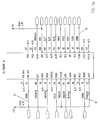
- Fig. 1 shows socket 10 with terminal 26 carrying signal IGNNE*, terminal 27 carrying signal FERR1*, terminal 29 carrying signal FERR*, and terminal 21 carrying signal NMI.
- Signals PRO/COP* and DX*/SX are combined in AND gate 11 to gate signal NMI through buffer 12.
- the "*" is used to denote assertion of a low signal level.
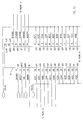
- Fig. 2 illustrates socket 10 with the necessary circuitry for enabling the redirection of specified signals to different pins, depending upon the type of processor used.
- PAL 18 is shown having output IGNNE*/NMI connected to pin a15 of processor 20. Pins c14 and a13 carries signals FERR* or FERR1*, respectively, to PAL 18.
- PAL 18, in this preferred embodiment, is a type 16R4-7. PAL 18 redirects signal FERR* (and FERR1*, as designated for the type 80487SX) when required.
- signals NMI, and IGNNE* are required to be redirected.
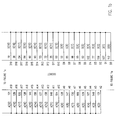
- One of signals FERR* and FERR1* is selected depending upon the type of processor. The following table illustrates the map for these signals.
- BIOS 15 of any of the processors includes a program for detecting the processor type when the computer system ist powers up.
- the ID is provided by the processor itself and the program supplied by the BIOS 15 codes that ID into a two bit binary code and stores it in register 16.
- BIOS 15 also has a program for detecting the presence or absence of a coprocessor, thereby adding to the identification of the processor. This formation is coded into one bit in register 16 and is shown as signal PRO/COP*.
- the ID is shown as signal DX*/SX from BIOS 15 into register 16.
- the programs for determining this full identification are listed below.
- the NMI signal for types 80486DX and 80487SX are applied to pin B15 through buffer 12 by the gating signal from register 16, as shown. If, however, the processor is type 80486SX, then signal NMI is applied to pin A15 via PAL 18, as shown. Signal IGNNE* is applied to pin A15 for types 80486DX and 80487SX and not connected for the type 80486SX.
- PAL 18 The operation of PAL 18 is described by the following:
- signal NMI When a type 80486DX processor is installed, signal NMI is gated through buffer 12 and impressed on pin B15.
- Signal IGNNE* is gated by the PAL to Pin A15.
- Pin C14 is scanned for its indication of signal FERR*. In this manner, it is shown that at least three different processors from the same family may each be installed in a single socket without the user having to take any further steps or precautions.
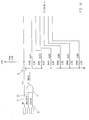
- Fig. 3 represents that part of the computer system which is capable of monitoring selected signals from the processor and of providing connections in accordance with those signals.
- the processor 20 is connected to its basic input/output system (BIOS) memory 15, the BIOS memory 15 is connected to a register 16 and the register 16 is connected to a gate 12 and to a programmable array logic (PAL) circuit 18.
- the PAL circuit 18 is connected to the pins A13, C14 and A15 of the processor 20.
- the gate 12 is connected to the pin B15 of the processor 20.
- the PAL circuit 18 has input signal lines IGNNE* and NMI and the gate 12 has an input signal line NMI.
- the PAL circuit 18 is capable of connecting pin A15 of the processor 20 either to the signal line IGNNE* or to the signal line NMI and the gate 12 is capable of connecting the signal line NMI to the pin B15 of the processor 20 or to blocking that connection.
- the PAL circuit 18 is controlled by data from the register 16 and by the signals FERR and FERR1 provided by the processor ports connected respectively to the pins C14 and A13.
- Table 1 shows that for an Intel Type 80486DX main processor, the signal FERR is provided at pin C14, the signal IGNNE is required at pin A15 and the signal NMI is required at pin B15.
- the signal IGNNE is not required and the signal NMI is required at pin A15.
- the signal FERR is provided at pin A13, the signal IGNNE is required at pin A15 and the signal NMI is required at pin B15.
- Fig. 3 can provide each of the three sets of conditions set out in Table 1.
Landscapes
- Engineering & Computer Science (AREA)
- Theoretical Computer Science (AREA)
- General Engineering & Computer Science (AREA)
- Physics & Mathematics (AREA)
- General Physics & Mathematics (AREA)
- Microelectronics & Electronic Packaging (AREA)
- Computer Hardware Design (AREA)
- Stored Programmes (AREA)
- Information Transfer Systems (AREA)
- Multi Processors (AREA)
- Connecting Device With Holders (AREA)
Applications Claiming Priority (2)
| Application Number | Priority Date | Filing Date | Title |
|---|---|---|---|
| US76687791A | 1991-09-27 | 1991-09-27 | |
| US766877 | 1991-09-27 |
Publications (2)
| Publication Number | Publication Date |
|---|---|
| EP0534770A2 true EP0534770A2 (de) | 1993-03-31 |
| EP0534770A3 EP0534770A3 (en) | 1994-11-09 |
Family
ID=25077795
Family Applications (1)
| Application Number | Title | Priority Date | Filing Date |
|---|---|---|---|
| EP9292308739A Withdrawn EP0534770A3 (en) | 1991-09-27 | 1992-09-25 | User transparent system for using any one of a family of processors in a single socket |
Country Status (4)
| Country | Link |
|---|---|
| US (1) | US5835750A (de) |
| EP (1) | EP0534770A3 (de) |
| JP (2) | JPH05204844A (de) |
| KR (1) | KR930006553A (de) |
Cited By (1)
| Publication number | Priority date | Publication date | Assignee | Title |
|---|---|---|---|---|
| DE4218787A1 (de) * | 1992-02-12 | 1993-08-26 | Samsung Electronics Co Ltd | Selbstschaltende einrichtung fuer eine zentraleinheits-logik |
Families Citing this family (10)
| Publication number | Priority date | Publication date | Assignee | Title |
|---|---|---|---|---|
| DE19700397C1 (de) * | 1997-01-08 | 1998-04-23 | Sgs Thomson Microelectronics | Schutzschaltung für programmgesteuerte elektrische Einrichtungen |
| US6226741B1 (en) * | 1998-04-03 | 2001-05-01 | Asustek Computer Inc. | Jumperless computer system |
| US6338639B1 (en) | 2000-05-09 | 2002-01-15 | Tyco Electronics Corporation | Lever actuated ZIF processor socket |
| US8071051B2 (en) * | 2004-05-14 | 2011-12-06 | Honeywell International Inc. | Portable sample analyzer cartridge |
| US6763478B1 (en) | 2000-10-24 | 2004-07-13 | Dell Products, L.P. | Variable clock cycle for processor, bus and components for power management in an information handling system |
| US6985987B2 (en) * | 2000-11-01 | 2006-01-10 | Via Technologies, Inc. | Apparatus and method for supporting multi-processors and motherboard of the same |
| US6988214B1 (en) | 2000-11-06 | 2006-01-17 | Dell Products L.P. | Processor power state transistions using separate logic control |
| US6735663B2 (en) | 2000-12-18 | 2004-05-11 | Dell Products L.P. | Combination personal data assistant and personal computing device |
| US8335879B2 (en) * | 2010-04-29 | 2012-12-18 | Hewlett-Packard Development Company, L.P. | Node differentiation in multi-node electronic systems |
| US10111334B1 (en) | 2017-03-30 | 2018-10-23 | Dell Products, L.P. | Information handling system interposer enabling specialty processor integrated circuit in standard sockets |
Family Cites Families (10)
| Publication number | Priority date | Publication date | Assignee | Title |
|---|---|---|---|---|
| JPH0248936B2 (ja) * | 1984-10-02 | 1990-10-26 | Fujitsu Ltd | Handotaishusekikairosochi |
| JPS62247275A (ja) * | 1986-03-31 | 1987-10-28 | Ando Electric Co Ltd | インサ−キツトエミユレ−タのcpu識別回路 |
| US4972470A (en) * | 1987-08-06 | 1990-11-20 | Steven Farago | Programmable connector |
| JPH01142967A (ja) * | 1987-11-30 | 1989-06-05 | Nec Corp | コプロセッサ制御方式 |
| US4967346A (en) * | 1988-03-14 | 1990-10-30 | Advanced Micro Devices, Inc. | Universal microprocessor interface circuit |
| US5134713A (en) * | 1989-05-19 | 1992-07-28 | Compaq Computer Corporation | Coprocessor detection circuit |
| US5109503A (en) * | 1989-05-22 | 1992-04-28 | Ge Fanuc Automation North America, Inc. | Apparatus with reconfigurable counter includes memory for storing plurality of counter configuration files which respectively define plurality of predetermined counters |
| US5321827A (en) * | 1989-08-02 | 1994-06-14 | Advanced Logic Research, Inc. | Computer system with modular upgrade capability |
| EP0510241A3 (en) * | 1991-04-22 | 1993-01-13 | Acer Incorporated | Upgradeable/downgradeable computer |
| DE69223209T2 (de) * | 1991-09-30 | 1998-06-18 | Toshiba Kawasaki Shi Kk | Rechnersystem mit austauschbarer CPU |
-
1992
- 1992-06-24 KR KR1019920010996A patent/KR930006553A/ko not_active Abandoned
- 1992-08-06 JP JP4210321A patent/JPH05204844A/ja active Pending
- 1992-09-25 EP EP9292308739A patent/EP0534770A3/en not_active Withdrawn
-
1996
- 1996-11-06 US US08/744,671 patent/US5835750A/en not_active Expired - Lifetime
-
2003
- 2003-07-31 JP JP2003004300U patent/JP2004000007U/ja active Pending
Cited By (1)
| Publication number | Priority date | Publication date | Assignee | Title |
|---|---|---|---|---|
| DE4218787A1 (de) * | 1992-02-12 | 1993-08-26 | Samsung Electronics Co Ltd | Selbstschaltende einrichtung fuer eine zentraleinheits-logik |
Also Published As
| Publication number | Publication date |
|---|---|
| EP0534770A3 (en) | 1994-11-09 |
| KR930006553A (ko) | 1993-04-21 |
| JP2004000007U (ja) | 2004-04-08 |
| JPH05204844A (ja) | 1993-08-13 |
| US5835750A (en) | 1998-11-10 |
Similar Documents
| Publication | Publication Date | Title |
|---|---|---|
| US4456790A (en) | Automated hardware inventory system | |
| EP0534770A2 (de) | Verbrauchertransparentes System zum Ermöglichen des Einsetzens jedes Prozessorfamilienmitglieds in eine einzige IC-Trägerfassung | |
| EP0263886B1 (de) | Unterbrechungssteuerungsverfahren in einem mehrprozessorsystem | |
| WO1999056217A1 (en) | Interrupt controller | |
| EP0041406B2 (de) | Bauteil-Identifikation in einem Rechnersystem | |
| KR920001814B1 (ko) | 다이렉트 메모리 액세스 제어장치 | |
| US5163145A (en) | Circuit for determining between a first or second type CPU at reset by examining upper M bits of initial memory reference | |
| JP2004000007U6 (ja) | ディジタルコンピュータシステム | |
| US4630212A (en) | Sewing machine with memory input reconfiguration based on type of memory being used | |
| CA1269177A (en) | System for maintaining the hardware-software compatibility of modular communication systems | |
| US4488257A (en) | Method for confirming incorporation of a memory into microcomputer system | |
| EP0239979B1 (de) | Vorrichtung zur Bestimmung der Prioritätsordnung | |
| US3348198A (en) | Code-checking comparator circuit | |
| KR19990023847A (ko) | 프로그래머블 제어기 시스템에서 베이스 보드와 그 위에 장착된 전원 유니트 및 cpu 유니트 | |
| CA1298412C (en) | Chip test condition selection method and apparatus | |
| EP0283847A3 (de) | Vorrichtung zum Auswählen einer Referenzzeile für Bilddatenkompression | |
| US5218606A (en) | Current-spare switching control system | |
| US4887268A (en) | Error checking apparatus | |
| KR100251554B1 (ko) | 스태킹 시스템의 자동 아이디 지정 장치 및 방법 | |
| KR950007107B1 (ko) | 별도의 마이크로프로세서를 포함하는 컴퓨터장치 | |
| EP0509720B1 (de) | Adresssteuerungsanordnung von Peripheriegeräten | |
| KR880002100B1 (ko) | 멀티프로세서 시스템(multiprocessor system) | |
| JPS60171540A (ja) | 集積回路 | |
| CA2063519A1 (en) | Automatic switching system for performing connection control between a plurarity of sets of subscriber terminals | |
| JPH11191090A (ja) | 情報処理装置 |
Legal Events
| Date | Code | Title | Description |
|---|---|---|---|
| PUAI | Public reference made under article 153(3) epc to a published international application that has entered the european phase |
Free format text: ORIGINAL CODE: 0009012 |
|
| AK | Designated contracting states |
Kind code of ref document: A2 Designated state(s): DE FR GB IT |
|
| PUAL | Search report despatched |
Free format text: ORIGINAL CODE: 0009013 |
|
| AK | Designated contracting states |
Kind code of ref document: A3 Designated state(s): DE FR GB IT |
|
| 17P | Request for examination filed |
Effective date: 19950502 |
|
| 18D | Application deemed to be withdrawn |
Effective date: 19980401 |