EP0534702A1 - Système de surveillance en continue de décharge électrostatique - Google Patents
Système de surveillance en continue de décharge électrostatique Download PDFInfo
- Publication number
- EP0534702A1 EP0534702A1 EP92308585A EP92308585A EP0534702A1 EP 0534702 A1 EP0534702 A1 EP 0534702A1 EP 92308585 A EP92308585 A EP 92308585A EP 92308585 A EP92308585 A EP 92308585A EP 0534702 A1 EP0534702 A1 EP 0534702A1
- Authority
- EP
- European Patent Office
- Prior art keywords
- limit value
- input path
- current source
- voltage
- terminal
- Prior art date
- Legal status (The legal status is an assumption and is not a legal conclusion. Google has not performed a legal analysis and makes no representation as to the accuracy of the status listed.)
- Granted
Links
Images


Classifications
-
- G—PHYSICS
- G01—MEASURING; TESTING
- G01R—MEASURING ELECTRIC VARIABLES; MEASURING MAGNETIC VARIABLES
- G01R31/00—Arrangements for testing electric properties; Arrangements for locating electric faults; Arrangements for electrical testing characterised by what is being tested not provided for elsewhere
- G01R31/50—Testing of electric apparatus, lines, cables or components for short-circuits, continuity, leakage current or incorrect line connections
- G01R31/54—Testing for continuity
-
- G—PHYSICS
- G01—MEASURING; TESTING
- G01R—MEASURING ELECTRIC VARIABLES; MEASURING MAGNETIC VARIABLES
- G01R31/00—Arrangements for testing electric properties; Arrangements for locating electric faults; Arrangements for electrical testing characterised by what is being tested not provided for elsewhere
- G01R31/50—Testing of electric apparatus, lines, cables or components for short-circuits, continuity, leakage current or incorrect line connections
- G01R31/52—Testing for short-circuits, leakage current or ground faults
Definitions
- This invention pertains generally to electrostatic discharge monitoring systems and more particularly to an electrostatic discharge continuous monitoring system adapted to provide a static safe work area.
- ground straps which are connected to a ground, are connected to electrically conductive wrist bands worn by operators in the work area. Work surfaces, such as a work bench, and floor mats are grounded to an electric ground. As the operator moves about the work area, the ground strap provides a path to ground to dissipate electrostatic charges that are generated by movement of the workers.
- Another object of this invention is to provide a static safe work area.
- Still another object of this invention is to provide electrostatic discharge protection during fault or shorted conditions, the result of which may be harmful to a worker or the product.
- a monitoring system including a connector, having an input path and a current return path, for connecting a two section wrist strap to said connector, said two section wrist strap, when affixed to an operator's wrist, would complete an electrical path between the input path and the current return path of the connector across the wrist skin surface.
- the monitoring system further includes a current source for providing an electrical current to the input path and means for connecting a resistor within the current return path to provide a voltage at the input path.
- the monitoring system also includes a comparator for comparing the voltage at the input path to a high limit value and a low limit value and for providing an alarm signal whenever the predetermined voltage at the input path is not between the high limit value and the low limit value.
- a further aspect of the present invention includes the method of ensuring an operator is properly connected to a ground potential for protecting circuit elements from electrostatic discharges between the operator and ground including the steps of coupling a two section strap having an input path and an output path to the operator such that the operator completes a signal path between the input path and the output path of the two section strap.
- the method further includes providing a predetermined electrical current to the input path of the two section strap and connecting a bleeding resistor between the output path of the two section strap and an electrical current return path for providing a predetermined voltage at the input path of the two section strap.
- the method also includes comparing continuously the predetermined voltage at the input path of the two section strap to a high limit value and a low limit value and providing an alarm signal whenever the predetermined voltage at the input path of the two section strap is not between the high limit value and the low limit value.
- FIG. 1 a block diagram of an electrostatic discharge (ESD) continuous monitoring system element 10 is shown to include a current source 20.
- the current source 20 provides an electrical current to an input path of a two section wrist band 12 (hereinafter referred to as wrist band 12) via a first terminal of a two terminal connector 16.
- the wrist band 12 having an input path and an output path is arranged to connect the input path to the output path when worn by a worker.
- the output path of the wrist band 12 is connected to a second terminal of the two terminal connector 16 through a resistor 14.
- the connector 16 is then connected to a resistor 18 which then in turn is connected to a current source path return.
- the resistor 14 is a 500 K ⁇ resistor and the resistor 18 is a 500 K ⁇ resistor.
- the current source 20 is a one microamp current source, thus providing one volt per each one meg ohm resistance in the current path.
- the output of the current source 20 is also connected to an input port of a comparator 22.
- a current path is provided producing an appropriate voltage at the input of the comparator 22.
- a light 24 is illuminated to indicate a safe or a pass status. If the voltage at the input of the comparator 22 is not between the high limit value and the low limit value then a light 26 is illuminated indicating a fail status and an alarm 28 is also activated.
- the high limit value is set for 1.5 volts and the low limit value is set for one volt
- the monitored resistance is less than one M ⁇ or more than 1.5 M ⁇
- the fail light 26 and the alarm 28 are activated.
- the pass light 24 is activated.
- an alarm is activated indicating the worker is not adequately protected.
- an appropriate current source could be fed to a solder pot through a bleeding resistor to ensure the solder pot was properly grounded.
- a floor mat, a work surface, or any other device in the work area could be connected appropriately to ensure they are properly grounded.
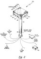
- a monitoring system 100 is shown to include a circuit box 30 mounted on a pedestal 32.
- the circuit box 30 houses electronic circuitry as to be described further hereinafter as well as a plurality of switches, S1, S2, S3, S4 and S5 which allow the worker to perform various tests as well as switching the monitoring system 100 off and on. Additionally, the circuit box 30 includes a plurality of lights DS1, DS2, DS3 and DS4 which indicate various status conditions. Also an audio alarm is provided.
- various wires extend to make connections to various devices around the work station, for example, to a solder pot, to a work surface, to a floor mat and to a connection box 40 wherein a worker and a supervisor can be connected to the monitoring system 100.
- connection to a reference ground is made as well as a connection to an AC power outlet, via a power supply 50.
- a test probe 34 is also provided to allow the worker to test a hot solder iron to ensure the solder iron is properly grounded.
- a nine-volt DC power line is provided, via terminals of a connector J4, from the power supply 50 (FIG. 2), here from a nine-volt DC power supply such as a Switchcraft PC-712A, manufactured by Switchcraft, Inc. located in Chicago, IL.
- the switch S5 is provided in line with the nine-volt DC power line to turn the monitoring system 100 on and off.
- a 0.47 microfarad capacitor C20 is provided between the nine-volt DC power line and ground.
- the nine-volt DC power line is fed to an input of a five-volt power supply regulator Z8, here provided by a LM78M05CP integrated circuit, wherein the output thereof provides a five-volt DC signal.
- a 0.47 microfarad capacitor C21 is connected between the output of the five-volt power supply regulator Z8 and ground.
- the five-volt DC signal is then fed, via connector P1A and J1A, to the various integrated circuits throughout the electronic circuit to provide the required five-volt DC signal.
- the monitoring system 100 provides monitoring capability for a worker, a supervisor, a floor mat, a work surface, a solder pot and a solder iron. As such, the monitoring system 100 requires six current sources, here four one microamp constant current sources and two fifty milliamp constant current sources as to be described.
- a voltage divider network 101 is provided by connecting a 1.0 K ⁇ resistor R1 in series with a 4.0 K ⁇ resister R2 between the five-volt DC signal and ground. As such a 4 volt DC signal is provided at a connection between the resistor R1 and resistor R2.
- the four volt DC signal is fed to a first input of an operational amplifier Z1B, here provided by an LM358AN type integrated circuit which also provides an operational amplifier Z1A.
- An integrated circuit Z3, here an MPQ2907 type integrated circuit provides four PNP transistors. The output of the operational amplifier Z1B is fed to the base of each of the PNP transistors.
- each of the transistors are connected to the five-volt DC signal via a one M ⁇ resistor R5, R6, R7, R8 respectively.
- the emitter of one of the transistors is also connected to a second input of the operation amplifier Z1B. With such an arrangement, the collector of each of the transistors provide a one microamp constant current source.
- the four-volt DC signal is also fed to a first input of the operational amplifier Z1A.
- An integrated circuit Z2, here also an MPQ2907, provides four PNP transistors of which two of the PNP transistors are not used.
- the output of the operational amplifier Z1A is fed to the base of the remaining two transistors.
- Each of the emitters of the transistors are connected to the five-volt power signal through a 20 ohm resistor R3, R4 respectively.
- the emitter of one of the transistors is connected to the second input of the operational amplifier Z1A as shown.
- the collector of one of the transistors is connected to an anode of diode CR1 having also a cathode.
- the cathode of diode CR1 is connected to an anode of diode CR2 having also a cathode.
- the cathode of diode CR2 is connected to ground.
- Diode CR1 and diode CR2 are here 1N458 type diodes.
- the collector of the other one of the transistors is connected to the anode of diode CR3 having also has a cathode.
- the cathode of diode CR3 is connected to an anode of a diode CR4 having also a cathode.
- the cathode of diode CR4 is connected to ground.
- Diode CR3 and diode CR4 are also IN458 type diodes. With such an arrangement, the collector of each of the transistors provide a 50 milliamp constant current source.
- Window comparators 22A, 22B, 22C and 22D associated respectively with each of the one microamp constant current sources each include an input and an output, with the outputs of the window comparators 22A, 22B, 22C and 22D connected together.
- a 15 K ⁇ resistor R24 is connected between the five-volt DC signal and the outputs of the window comparators 22A, 22B, 22C and 22D.
- a 0.47 microfarad capacitor C2 is connected between ground and the outputs of the window comparators 22A, 22B, 22C and 22D.
- the outputs of window comparators 22A, 22B 22C and 22D are also connected to a base connector of an NPN transistor Z7D.
- window comparator 22A the output of one of the one microamp constant current sources is connected to the input of the window comparator 22A.
- the window comparator 22A is adapted to provide an approximately five volt output signal when the voltage of an input signal is between an appropriate high limit value and an appropriate low limit value and to provide a near ground output signal when the voltage of the input signal is not between the appropriate high limit value and the appropriate low limit value.
- the appropriate high limit value is provided by a high voltage reference signal, V REF3 and the appropriate low limit value is provided by a low voltage reference signal V REF2 .
- the high voltage reference signal V REF3 and the low voltage reference signal V REF2 are provided by a voltage divider network 102.
- the voltage divider network 102 includes a 500 ⁇ variable resistor R28, a 499 ⁇ resistor R29, a 2 K ⁇ resistor R30 and a 2 K ⁇ resistor R31 connected in series between ground and the five-volt DC signal as shown.
- the high voltage reference signal V REF3 is provided at a connection between the resistor R30 and the resistor R31.
- the low voltage reference signal V REF2 is provided at a connection between the resistor R29 and the resistor R30.
- a variable output of the 500 ⁇ variable resistor R28 provides a variable voltage reference signal V REF1 .
- variable voltage reference signal V REF1 has a variable voltage from 0 volts to approximately 0.5001 volts, but is set to approximately 0.11 volts.
- the window comparator 22A includes a pair of operational amplifiers Z4A and Z4B, each having a first and second input and an output.
- the pair of operational amplifiers Z4A and Z4B are provided by an integrated circuit Z4, here a LM339AN type integrated circuit, having four operational amplifiers Z4A, Z4B, Z4C and Z4D disposed within.
- An input signal V IN1 to the window comparator 22A is fed, via a 10 K ⁇ resistor R12, to the first input of the operational amplifier Z4A and also to the second input of the operational amplifier Z4B.
- the high voltage reference signal V REF3 is fed through a 10 K ⁇ resistor R16 to the second input of the operational amplifier Z4A.
- the low voltage reference signal V REF2 is fed through a 10 K ⁇ resistor R17 to the first input of the operational amplifier Z4B.
- a 0.47 microfarad capacitor C10 is connected between the output and the first input of the operational amplifier Z4A.
- a 0.47 microfarad capacitor C6 is connected between the output and the first input of the operational amplifier Z4B.
- the output of the operational amplifier Z4A is approximately five volts. If the voltage of the input signal V IN1 is more positive than the voltage of the high voltage reference signal V REF3 , then the output of the operational amplifier Z4A is near ground. Furthermore, if the voltage of the input signal V IN1 is more positive than the voltage of the low voltage reference signal V REF2 , then the output of the operational amplifier Z4B is approximately five volts.
- the output of the operational amplifier Z4B is near ground. It should now be appreciated, when the voltage of the input signal V IN1 is equal to or greater than the voltage of the low voltage reference signal V REF2 and is equal to or lower than the voltage of the high voltage reference signal V REF3 , then the output signal of the window comparator 22A is approximately five volts. When the voltage of the input signal V IN1 is less than the voltage of the low voltage reference signal V REF2 or greater than the voltage of the high voltage reference signal V REF3 , then the output signal of the window comparator 22A is near ground.
- window comparator 22B includes a pair of operational amplifiers Z4C and Z4D, each having a first and second input and an output.
- An input signal V IN2 to the window comparator 22B is fed, via a 10 K ⁇ resistor R13, to the first input of the operational amplifier Z4C and also to the second input of the operational amplifier Z4D.
- the high voltage reference signal V REF3 is fed through a 10 K ⁇ resistor R18 to the second input of the operational amplifier Z4C.
- the low voltage reference signal V REF2 is fed through a 10 K ⁇ resistor R19 to the first input of the operational amplifier Z4D.
- a 0.47 microfarad capacitor C9 is connected between the output and the first input of the operational amplifier Z4C.
- a 0.47 microfarad capacitor C5 is connected between the output and the first input of the operational amplifier Z4D.
- the window comparator 22B operates in a manner similar to the window comparator 22A such that when the voltage of the input signal V IN2 is equal to or greater than the voltage of the low voltage reference signal V REF2 and is equal to or lower than the voltage of the high voltage reference signal V REF3 , then the output signal of the window comparator 22B is near five volts. When the voltage of the input signal V IN2 is less than the voltage of the low voltage reference signal V REF2 or greater than the voltage of the high voltage reference signal V REF3 , then the output signal of the comparator 22B is near ground.
- Window comparator 22C includes a pair of operational amplifiers Z5A and Z5B, each having a first and second input and an output.
- Window comparator 22D includes a pair of operational amplifiers Z5C and Z5D, each having a first and second input and an output.
- the operational amplifiers Z5A, Z5B, Z5C and Z5D are provided by an integrated circuit Z5, here an LM339AN type integrated circuit.
- An input signal V IN3 to the window comparator 22C is fed, via a 10 K ⁇ resistor R14, to the first input of the operational amplifier Z5A and also to the second input of the operational amplifier Z5B.
- the high voltage reference signal V REF3 is fed through a 10 K ⁇ resistor R20 to the second input of the operational amplifier Z5A.
- the low voltage reference signal V REF2 is fed through a 10 K ⁇ resistor R21 to the first input of the operational amplifier Z5B.
- a 0.47 microfarad capacitor C8 is connected between the output and the first input of the operational amplifier Z5A.
- a 0.47 microfarad capacitor C4 is connected between the output of the first input of the operational amplifier Z5B.
- An input signal V IN4 to the window comparator 22D is fed, via a 10 K ⁇ resistor R15, to the first input of the operational amplifier Z5C and also to the second input of the operational amplifier Z5D.
- the high voltage reference signal V REF3 is fed through a 10 K ⁇ resistor R22 to the second input of the operational amplifier Z5C.
- the low voltage reference signal V REF2 is fed through a 10 K ⁇ resistor R23 to the first input of the operational amplifier Z5D.
- a 0.47 microfarad capacitor C7 is connected between the output and the first input of the operational amplifier Z5C.
- a 0.47 microfarad capacitor C3 is connected between the output and the first input of the operational amplifier Z5D.
- the window comparator 22C and the window comparator 22D operate in a manner similar to the window comparator 22A.
- the voltage at the base connector of the NPN transistor Z7D is approximately five volts to turn the NPN transistor Z7D on as described further hereinafter.
- Comparators 22E and 22F are associated with the two fifty milliamp constant current sources.
- An integrated circuit here a LM339AN type integrated circuit, provides four operational amplifiers including operational amplifiers Z6A and Z6B, each having a first and second input and an output. The other two operational amplifiers are not used.
- the comparator 22E includes the operational amplifier Z6A with a 0.47 microfarad capacitor C1 connected between the output and the first input of the operational amplifier Z6A.
- An input signal V IN5 to the comparator 22E is fed, via a 10 K ⁇ resistor R11, to the first input of the operational amplifier Z6A.
- the variable voltage reference signal V REF1 is fed through a 10 K ⁇ resistor R10 to the second input of the operational amplifier Z6A.
- the output of the operational amplifier Z6A is fed to a base connector of an NPN transistor Z7A.
- the comparator 22F includes the operational amplifier Z6B with a 0.47 microfarad capacitor C11 connected between the output and the first input of the operational amplifier Z6B.
- An input signal V IN6 to the comparator 22F is fed, via a 10 K ⁇ resistor R25, to the first input of the operational amplifier Z6A.
- the variable voltage reference signal V REF1 is fed through a 10 K ⁇ resistor R26 to the second input of the operational amplifier Z6B.
- the output of the operational amplifier Z6B is fed to the base connector of the NPN transistor Z7D.
- Comparators 22E and 22F are adapted to provide an approximately five volt output signal when the voltage of the respective input signal V IN5 , V IN6 is less than or equal to the voltage of the variable voltage reference signal V REF1 .
- the comparators 22E and 22F are adapted to provide a near ground output signal when the voltage of the respective input signal V IN5 , V IN6 is greater than the voltage of the variable voltage reference signal V REF1 .
- the outputs of the window comparators 22A, 22B, 22C and 22D and the output of the comparator 22F are connected to the base connector of the NPN transistor Z7D.
- An integrated circuit 27, here an MPQ2222 type integrated circuit provides four NPN transistors Z7A, Z7B, Z7C and Z7D, each having an emitter, a collector and a base connector.
- the NPN transistor Z7D is arranged such that the emitter connection is connected to ground and the collector connection is connected to a first terminal of a light DS1, via a terminal of the connectors J1A and P1A.
- the light DS1, having the first terminal and a second terminal is a green light when illuminated.
- the second terminal of the light DS1 is connected to the five-volt DC signal.
- the NPN transistors Z7D will conduct, completing a current path to ground for the light DS1, illuminating the light DS1. If a near ground potential is fed to the base connector of the NPN transistor Z7D, the NPN transistor Z7D will not conduct, breaking the current path to ground for the light DS1 so that the light DS1 is not illuminated.
- the NPN transistor Z7C is arranged such that the emitter connection is connected to ground and a 5.1 K ⁇ resistor R27 is connected between the base connection of the NPN transistor Z7C and the collector connection of the NPN transistor Z7D.
- the collector connection of the NPN transistor Z7C is connected to a first terminal of a light DS2, via a terminal of the connectors J1A and P1A.
- the light DS2, having the first terminal and a second terminal, is a red light when illuminated.
- the second terminal of the light DS2 is connected to the five-volt DC signal.
- the first terminal of the light DS2 is also connected to an input of a switch S1 having also an output.
- the output of the switch S1 is connected to a first terminal of an audible alarm (not numbered) having also a second terminal.
- the second terminal of the audible alarm is connected to the five-volt DC signal.
- the NPN transistor Z7C will not conduct, breaking the current path to ground for the light DS2 so that the light DS2 is not illuminated.
- a near ground potential is fed to the base connection of the NPN transistor Z7C so that the NPN transistor Z7C is not conducting.
- an approximately five volt potential is fed to the base connection of the NPN transistor Z7C so that the NPN transistor Z7C is conducting.
- the monitoring system 100 also includes the NPN transistor Z7A and the NPN transistor Z7B arranged in a manner similar to the NPN transistor Z7C and the NPN transistor Z7D.
- the emitter connection of the NPN transistor Z7A is connected to ground and the emitter connection of the NPN transistor Z7B is connected to ground.
- a 5.1 K ⁇ resistor R32 is connected between the collector connection of the NPN transistor Z7A and the base connection of the NPN transistor Z7B.
- a 1 K ⁇ resistor R9 is connected between the base connection of the NPN transistor Z7A and the five-volt DC signal.
- the collector connection of the NPN transistor Z7A is also connected, via a terminal of the connectors J1A and P1A, to a first terminal of a light DS4 having also a second terminal.
- the light DS4 is a green light when illuminated.
- the second terminal of the light DS4 is connected to the five-volt DC signal.
- the collector connection of the NPN transistor Z7B is connected, via a terminal of the connectors J1A and P1A, to a first terminal of a light DS3 having also a second terminal.
- the light DS3 is a red light when illuminated.
- the second terminal of the light DS3 is connected to the five-volt DC signal.
- the NPN transistor 7A When the NPN transistor 7A is not conducting, an approximately five volt potential is fed to the base connection of the NPN transistor Z7B. If an approximately five volt potential is fed to the base connection of the NPN transistor Z7B, the NPN transistor Z7B will conduct, completing a current path to ground for the light DS3 so that the light DS3 is illuminated. If a near ground potential is fed to the base connector of the NPN transistor Z7B, the NPN transistor Z7B will not conduct, breaking the current path to ground for the light DS3 so that the light DS3 is not illuminated.
- the NPN transistor Z7A will conduct completing a current path to ground for the light DS4 so that the light DS4 is illuminated. If a near ground potential is fed to the base connector of the NPN transistor Z7A, the NPN transistor Z7A will not conduct breaking the current path to ground for the light DS4 so that the light DS4 is not illuminated. When the NPN transistor Z7A is conducting, a near ground potential is fed to the base connection of the NPN transistor Z7B.
- each of the fifty milliamp current sources is connected to an input of a corresponding one of the comparators 22E and 22F.
- the output of one of the fifty milliamp current sources is also connected, via a terminal of the connectors J1B and P1B, to an input of a first pole of a two pole double throw switch S2.
- the switch S2 having a first pole and a second pole with each pole having an input and a first and second output, is arranged such that the first pole is in a normally closed position between the input and the first output and the second pole is in a normally closed position between the input and the first output.
- the first output of the first pole of switch S2 is connected to a connector J6, which is used to connect a solder pot (not shown) to the monitoring system 100.
- a connector J6 which is used to connect a solder pot (not shown) to the monitoring system 100.
- the voltage of the input signal V IN6 is controlled by the amount of resistance between the connector J6 and ground. If the connector J6 is connected to a properly grounded solder pot, then the amount of resistance between the connector J6 and ground is minimal and the voltage of the input signal V IN6 is minimal. If the connector J6 is connected to an improperly connected solder pot, then the voltage of the input signal V IN6 varies in accordance with the amount of resistance between the connector J6 and ground.
- the fifty milliamp current source provides fifty milliamps of current
- the amount of resistance between the connector J6 and ground is less than 2.2 ohms
- the voltage of the input signal V IN6 is less than the voltage of the variable reference signal V REF1 and the output of the comparator 22F is an approximately five volt potential. If the amount of resistance between the connector J6 and ground is more than 2.2 ohms, then the voltage of the input signal V IN6 is greater than the voltage of the variable reference signal V REF1 and the output of the comparator 22F is near ground.
- the light DS1 is illuminated and the light DS2 is not illuminated. If the resistance between the connector J6 and ground is greater than 2.2.ohms, then the light DS1 is not illuminated and the light DS2 is illuminated and when the switch S1 is closed, the audible alarm is activated, warning the worker of an improper condition.
- the output of the other one of the fifty milliamp current sources is also connected, via a terminal of the connectors J1B and P1B, to the input of the second pole of switch S2.
- the first output of the second pole of switch S2 is connected to a connector J7.
- the connector J7 is used to connect the solder iron test probe 34 (FIG. 2) to the monitoring system 100.
- the voltage of the input signal V IN5 is controlled by the amount of resistance between the connector J7 and ground.
- the amount of resistance between the connector J7 and ground in large and the voltage of the input signal V IN5 is large. Since the fifty milliamp current source provides fifty milliamps of current, if the amount of resistance between the connector J7 and ground is less than 2.2 ohms, then the voltage of the input signal V IN5 is less than the voltage of the variable reference signal V REF1 and the output of the comparator 22E is an approximately five volt potential. If the amount of resistance between the connector J7 and ground is more than 2.2 ohms, then the voltage of the input signal V IN5 is greater than the voltage of the variable reference signal V REF1 and the output of the comparator 22E is near ground.
- the light DS4 is illuminated and the light DS3 is not illuminated indicating a properly grounded solder iron to the worker. If the resistance between the connector J7 and ground is greater than 2.2 ohms, then the light DS4 is not illuminated and the light DS3 is illuminated warning the worker of an improper condition.
- the switch S2 is provided to allow the worker to test the above described conditions.
- a 2 ⁇ resistor R40 is connected between the second output of the first pole of the switch S2 and ground.
- a 2 ⁇ resistor R41 is connected between the second output of the second pole of the switch S2 and ground.
- each one of the one microamp current sources is connected to an input of a corresponding one of the window comparators 22A, 22B, 22C and 22D.
- the output of one of the one microamp current sources is connected, via a terminal of the connectors J1B and P1B, to an input of a first pole of a switch S3.
- the switch S3 is a double pole, double throw switch having a first and second pole with each pole having an input and a first and second output.
- the switch S3 is arranged so that the first and second pole is normally in a closed position between the input and the first output of each pole.
- the first output of the first pole of switch S3 is connected via corresponding terminals of a connector J2 and a connector P2 to a jack J8, disposed on connection box 40 (FIG. 2), which is used to connect a worker or operator (not shown) to the monitoring system 100.
- the jack J8 having a first, a second and a third connector is adapted so that the first connector is connected to the second connector when a plug (not shown) is not mated with the jack J8, and when a plug (not shown) is mated with a jack J8, the connection between the first connector and the second connector is broken.
- the plug (not shown) having a first and a second connector is adapted, when mated with the jack J8, so that the first connector of the plug is connected to the first connector of the jack J8 and the second connector of the plug is connected to the third connector of the jack J8.
- the second connector of the jack J8 is connected to a 1.5 M ⁇ resistor R51 which is connected in series to ground via corresponding terminals of the connectors P2 and J2.
- the third connector of the jack J8 is connected to a 510 K ⁇ resistor R52 which is connected in series to ground via the connectors P2 and J2.
- the second output of the first pole of switch S3 is connected to a 510 K ⁇ resistor R42 which is connected in series to ground.
- the 1.5 M ⁇ resistor R51 is in the signal path between the one microamp current source and ground providing a corresponding voltage for the input signal V IN1 to the window comparator 22A.
- the resistance provided between the first connector and the third connector of the jack J8 and the 510 K ⁇ resistor R52 is in the signal path between the output of the one microamp current source and ground providing an corresponding voltage for the input signal V IN1 to the input of the window comparator 22A.
- the first connector and the second connector of the plug, which is mated with the jack J8, is connected to a 500 K ⁇ resistor in series with a two-section wrist strap which is attached to the worker.
- the output of a second one of the one microamp current sources is connected, via a terminal of the connectors J1B and P1B, to the input of the second pole of the switch S3.
- the first output of the second pole of the switch S3 is connected, via corresponding terminals of the connector J2 and the connector P2, to a first connection of a jack J9 disposed on connection box 40 (FIG. 2) which is used to connect a supervisor or a second worker (not shown) to the monitoring system 100.
- the jack J9 having the first, a second and a third connector is similar to the jack J8 and is adapted so that the first connector is connected to the second connector when a plug (not shown) is not mated with a jack J9 and when a plug (not shown) is mated with the jack J9 the connection between the first connector and the second connector is broken.
- the second connection of the jack J9 is connected to a 1.5 M ⁇ resistor R53 which is connected in series, via the connectors P2 and J2, to ground.
- the third connection of the jack J9 is connected to a 510 K ⁇ resistor R54 which is connected in series to ground.
- the light DS2 is illuminated indicating an improper condition.
- shock protection to the worker in the event of a wrist strap failure is provided.
- the total resistance in the current path through the wrist strap is less than 3 M ⁇ but if hair, dry skin or any other fault prevents a proper connection of the wrist strap, the resistance will exceed 3 M ⁇ and the light DS2 is illuminated.
- a supervisor is provided shock protection in the event of a wrist strap failure with the above-described circuit for the supervisor which operates similar to the circuit described for the worker.
- the switch S3 is provided to allow the worker to test the wrist band circuitry. When the switch S3 is not thrown, the first pole and second pole of the switch S3 are disposed with the input of each pole connected to the respective first output.
- each input is connected to the respective second output of each pole.
- the 510 K ⁇ resistor R42 and the 510 K ⁇ resistor R43 are in each respective current path between the respective one-microamp current source and ground so that the light DS2 is illuminated and the light DS1 is not illuminated.
- the output of a third one of the one microamp current sources is connected, via a terminal of the connectors J1B and P1B, to an input of a first pole of a switch S4.
- the switch S4 is a double pole, double throw switch having a first and a second pole with each pole having an input and a first and a second output.
- the switch S4 is arranged such that the first pole and the second pole are normally in a closed position between the input and the first output, respectively.
- the first output of the first pole of switch S4 is connected, via a terminal of a connector J3, to a work surface (not shown).
- the work surface is connected via another terminal of the connector J3 to ground.
- the second output of the first pole of switch S4 is connected to a 510 K ⁇ resistor which is connected in series to ground. With such an arrangement, the work surface is connected to the monitoring system 100.
- the output of the fourth one of the one microamp current sources is connected, via a terminal of the connectors J1B and P1B, to the input of the second pole of the switch S4.
- the first output of the second pole of the switch S4 is connected, via a terminal of the connector J3, to a floor mat (not shown).
- the floor mat is also connected, via another terminal of the connector J3, to ground.
- the second output of the second pole of the switch S3 is connected to a 510 K ⁇ resistor R45 which is connected in series to ground. With such an arrangement, the floor mat is connected to the monitoring system 100.
- the work surface and the floor mat are connected to the monitoring system 100 such that each provides between 1.0 M ⁇ and 3 M ⁇ resistance in the respective current path between a corresponding one-microamp current source and ground.
- the switch S4 is provided to allow the worker to test the corresponding circuitry. When the switch S4 is not thrown, the work surface and the floor mat are disposed in the respective current paths and the light DS1 is illuminated. When the switch S4 is thrown, the 510 K ⁇ resistor R44 and the 510 K ⁇ resistor R45 are disposed in the respective current paths and the light DS2 is illuminated. Thus by activating switch S4, the worker is ensured the lights DS1 and DS2 are operating correctly with the above-described circuitry.
- the monitoring system 100 is adapted to provide an alarm when a worker is not properly grounded or when various devices in the work station are not properly grounded thus reducing the possibility of an electrostatic discharge harming an electronic component. Furthermore, in the open circuit condition, the voltage provided to the operator is below that which is harmful.
Landscapes
- Physics & Mathematics (AREA)
- General Physics & Mathematics (AREA)
- Measurement Of Current Or Voltage (AREA)
- Emergency Alarm Devices (AREA)
- Elimination Of Static Electricity (AREA)
- Testing Of Short-Circuits, Discontinuities, Leakage, Or Incorrect Line Connections (AREA)
Applications Claiming Priority (2)
| Application Number | Priority Date | Filing Date | Title |
|---|---|---|---|
| US76716291A | 1991-09-27 | 1991-09-27 | |
| US767162 | 1991-09-27 |
Publications (2)
| Publication Number | Publication Date |
|---|---|
| EP0534702A1 true EP0534702A1 (fr) | 1993-03-31 |
| EP0534702B1 EP0534702B1 (fr) | 1998-09-02 |
Family
ID=25078664
Family Applications (1)
| Application Number | Title | Priority Date | Filing Date |
|---|---|---|---|
| EP92308585A Expired - Lifetime EP0534702B1 (fr) | 1991-09-27 | 1992-09-21 | Système de surveillance en continue de décharge électrostatique |
Country Status (5)
| Country | Link |
|---|---|
| US (1) | US5422630A (fr) |
| EP (1) | EP0534702B1 (fr) |
| JP (1) | JPH05205895A (fr) |
| CA (1) | CA2076488A1 (fr) |
| DE (1) | DE69226836T2 (fr) |
Cited By (4)
| Publication number | Priority date | Publication date | Assignee | Title |
|---|---|---|---|---|
| EP0981757A1 (fr) * | 1997-05-16 | 2000-03-01 | Northrop Grumman Corporation | Circuits avec mode test sur bande bracelet |
| WO2002010781A1 (fr) * | 2000-07-29 | 2002-02-07 | Newson Gale Limited | Dispositif de surveillance de resistance electrique |
| FR2863754A1 (fr) * | 2003-12-12 | 2005-06-17 | Valeo Electronique Sys Liaison | Procede et dispositif de detection d'au moins deux modes de fonctionnement d'un organe electrique d'un vehicule automobile, procede de pilotage de l'organe |
| US8476913B2 (en) | 2007-05-17 | 2013-07-02 | Newson Gale Limited | Improvements relating to the testing of an earth connection |
Families Citing this family (38)
| Publication number | Priority date | Publication date | Assignee | Title |
|---|---|---|---|---|
| US5666106A (en) * | 1996-09-04 | 1997-09-09 | Micron Electronics, Inc. | Accessway with grounding sensor |
| US5969626A (en) * | 1996-10-09 | 1999-10-19 | Altera Corporation | ESD ground monitor for electrostatic safe work tables |
| US5952931A (en) * | 1997-01-07 | 1999-09-14 | Seagate Technology, Inc. | Checker box of wrist-strap monitoring |
| EP1019739A1 (fr) * | 1997-07-17 | 2000-07-19 | Semtronics Corporation | Systeme de controle pour bande de poignet induisant une tension nulle |
| US6078875A (en) * | 1997-08-20 | 2000-06-20 | Semtronics Corporation | Automated auditing system |
| US6052053A (en) * | 1997-10-22 | 2000-04-18 | Semtronics Corporation | Continuous monitoring system |
| US6529955B1 (en) | 1999-05-06 | 2003-03-04 | Cisco Technology, Inc. | Proxy session count limitation |
| USD433193S (en) * | 1999-08-18 | 2000-10-31 | The Procter & Gamble Company | Sprayer |
| US6682004B2 (en) | 1999-08-18 | 2004-01-27 | The Procter & Gamble Company | Electrostatic spray device |
| US6814318B2 (en) | 1999-08-18 | 2004-11-09 | The Procter & Gamble Company | Disposable cartridge for electrostatic spray device |
| US6514504B1 (en) | 1999-08-18 | 2003-02-04 | The Procter & Gamble Company | Discontinuous films from skin care compositions |
| US6558682B2 (en) | 1999-08-18 | 2003-05-06 | The Procter & Gamble Company | Discontinuous films from skin care compositions |
| US7078046B1 (en) | 1999-08-18 | 2006-07-18 | The Procter & Gamble Company | Electrostatically-sprayable topical compositions having insulating external phase and conductive internal phase |
| US7152817B2 (en) * | 1999-08-18 | 2006-12-26 | The Procter & Gamble Company | Electrostatic spray device |
| US6311903B1 (en) | 1999-08-18 | 2001-11-06 | The Procter & Gamble Company | Hand-held electrostatic sprayer apparatus |
| US6531142B1 (en) | 1999-08-18 | 2003-03-11 | The Procter & Gamble Company | Stable, electrostatically sprayable topical compositions |
| US7712687B2 (en) * | 1999-08-18 | 2010-05-11 | The Procter & Gamble Company | Electrostatic spray device |
| US6318647B1 (en) | 1999-08-18 | 2001-11-20 | The Procter & Gamble Company | Disposable cartridge for use in a hand-held electrostatic sprayer apparatus |
| US6510987B1 (en) * | 2000-08-07 | 2003-01-28 | Advanced Micro Devices, Inc. | Automated monitoring of ESD (electro static discharge) of each of a plurality of operators in a production area |
| US6414600B1 (en) * | 2000-11-06 | 2002-07-02 | Advanced Micro Devices, Inc. | Ground check system for delta-flex test handler |
| US6850403B1 (en) | 2001-11-30 | 2005-02-01 | Ion Systems, Inc. | Air ionizer and method |
| US20030107379A1 (en) * | 2001-12-10 | 2003-06-12 | Weil Geoffrey M. | System and method for monitoring and controlling electrostatic charge |
| JP4680195B2 (ja) * | 2004-06-25 | 2011-05-11 | スパンション エルエルシー | 半導体装置及びソース電圧制御方法 |
| US7525316B2 (en) * | 2005-09-06 | 2009-04-28 | 3M Innovative Properties Company | Electrostatic discharge event and transient signal detection and measurement device and method |
| US7869182B1 (en) | 2006-08-23 | 2011-01-11 | Western Digital Technologies, Inc. | Monitoring device for use with an insulated dual portion garment |
| US7900272B1 (en) | 2006-08-23 | 2011-03-08 | Western Digital Technologies, Inc. | Static control garment |
| US7671599B1 (en) | 2007-01-31 | 2010-03-02 | Western Digital Technologies, Inc. | Static electricity monitor comprising a walking footpad electrode and handrail electrode |
| US7817057B2 (en) * | 2007-11-30 | 2010-10-19 | Hitachi Global Storage Technologies Netherlands B.V. | Wrist strap monitor remote alarm panel display |
| US20090167546A1 (en) * | 2007-12-26 | 2009-07-02 | Hsin-Ming Yang | Grounding Monitoring Device For Work Station Operator |
| US8138937B2 (en) * | 2007-12-26 | 2012-03-20 | Hsin-Ming Yang | Grounding monitoring device and system for work |
| US20100051502A1 (en) * | 2008-09-04 | 2010-03-04 | 3M Innovative Properties Company | Carrier having integral detection and measurement of environmental parameters |
| US20110227738A1 (en) * | 2010-03-18 | 2011-09-22 | Mcilroy Guy T | Wearable electronic ground integrity monitor |
| TWI431284B (zh) * | 2010-04-15 | 2014-03-21 | Tony Sheng Lin | 一種可以機動調設功能的工作檯接地監測方法及其裝置 |
| US8866629B2 (en) | 2011-05-04 | 2014-10-21 | International Business Machines Corporation | Built-in automated electrostatic discharge monitor for computing units |
| US8963552B2 (en) | 2012-04-26 | 2015-02-24 | 3M Innovative Properties Company | Electrostatic discharge event detector |
| CN103884951B (zh) * | 2012-12-21 | 2016-08-10 | 纬创资通股份有限公司 | 静电防护装置监控电路及静电防护装置监控系统 |
| CN104655970A (zh) * | 2013-11-19 | 2015-05-27 | 佛山市顺德区顺达电脑厂有限公司 | 夹具检测装置及检测方法 |
| US10203357B2 (en) | 2017-06-01 | 2019-02-12 | Seagate Technology Llc | Dynamic body voltage testing |
Citations (5)
| Publication number | Priority date | Publication date | Assignee | Title |
|---|---|---|---|---|
| DE3235660A1 (de) * | 1982-09-27 | 1984-03-29 | Siemens AG, 1000 Berlin und 8000 München | Schaltungsanordnung zur ueberwachung eines elektrischen messfuehlers auf unterbrechung und ueberbrueckung |
| US4649374A (en) * | 1984-01-06 | 1987-03-10 | Spectrascan, Inc. | Electrostatic system monitor and method therefor |
| US4800374A (en) * | 1986-10-31 | 1989-01-24 | Cray Research, Inc. | Personnel antistatic test device |
| EP0407186A2 (fr) * | 1989-07-06 | 1991-01-09 | Minnesota Mining And Manufacturing Company | Contrôleur de poste de travail |
| US5083117A (en) * | 1988-06-07 | 1992-01-21 | Hoigaard Jan C | Apparatus for monitoring and controlling electrostatic discharge |
Family Cites Families (2)
| Publication number | Priority date | Publication date | Assignee | Title |
|---|---|---|---|---|
| US4710751A (en) * | 1986-04-24 | 1987-12-01 | Environmental Protection Systems | Ground fault monitor circuit |
| US4785294A (en) * | 1986-06-24 | 1988-11-15 | Zero Corporation | Static monitoring system |
-
1992
- 1992-08-20 CA CA002076488A patent/CA2076488A1/fr not_active Abandoned
- 1992-09-21 DE DE69226836T patent/DE69226836T2/de not_active Expired - Fee Related
- 1992-09-21 EP EP92308585A patent/EP0534702B1/fr not_active Expired - Lifetime
- 1992-09-28 JP JP4258499A patent/JPH05205895A/ja active Pending
-
1994
- 1994-09-06 US US08/302,072 patent/US5422630A/en not_active Expired - Fee Related
Patent Citations (5)
| Publication number | Priority date | Publication date | Assignee | Title |
|---|---|---|---|---|
| DE3235660A1 (de) * | 1982-09-27 | 1984-03-29 | Siemens AG, 1000 Berlin und 8000 München | Schaltungsanordnung zur ueberwachung eines elektrischen messfuehlers auf unterbrechung und ueberbrueckung |
| US4649374A (en) * | 1984-01-06 | 1987-03-10 | Spectrascan, Inc. | Electrostatic system monitor and method therefor |
| US4800374A (en) * | 1986-10-31 | 1989-01-24 | Cray Research, Inc. | Personnel antistatic test device |
| US5083117A (en) * | 1988-06-07 | 1992-01-21 | Hoigaard Jan C | Apparatus for monitoring and controlling electrostatic discharge |
| EP0407186A2 (fr) * | 1989-07-06 | 1991-01-09 | Minnesota Mining And Manufacturing Company | Contrôleur de poste de travail |
Non-Patent Citations (1)
| Title |
|---|
| ELECTRONIC ENGINEERING vol. 58, no. 712, April 1986, LONDON GB page 34 A. BANDE ET AL. 'SINGLE CHIP CHECKS RESISTANCE' * |
Cited By (8)
| Publication number | Priority date | Publication date | Assignee | Title |
|---|---|---|---|---|
| EP0981757A1 (fr) * | 1997-05-16 | 2000-03-01 | Northrop Grumman Corporation | Circuits avec mode test sur bande bracelet |
| EP0981757A4 (fr) * | 1997-05-16 | 2000-03-01 | Northrop Grumman Corp | Circuits avec mode test sur bande bracelet |
| WO2002010781A1 (fr) * | 2000-07-29 | 2002-02-07 | Newson Gale Limited | Dispositif de surveillance de resistance electrique |
| GB2369447A (en) * | 2000-07-29 | 2002-05-29 | Newson Gale Ltd | Earthing device with resistance monitoring |
| GB2369447B (en) * | 2000-07-29 | 2004-06-23 | Newson Gale Ltd | Electrical resistance monitoring device |
| US6924740B2 (en) | 2000-07-29 | 2005-08-02 | Newson Gale Limited | Electrical resistance monitoring device |
| FR2863754A1 (fr) * | 2003-12-12 | 2005-06-17 | Valeo Electronique Sys Liaison | Procede et dispositif de detection d'au moins deux modes de fonctionnement d'un organe electrique d'un vehicule automobile, procede de pilotage de l'organe |
| US8476913B2 (en) | 2007-05-17 | 2013-07-02 | Newson Gale Limited | Improvements relating to the testing of an earth connection |
Also Published As
| Publication number | Publication date |
|---|---|
| JPH05205895A (ja) | 1993-08-13 |
| DE69226836D1 (de) | 1998-10-08 |
| EP0534702B1 (fr) | 1998-09-02 |
| DE69226836T2 (de) | 1999-04-22 |
| US5422630A (en) | 1995-06-06 |
| CA2076488A1 (fr) | 1993-03-28 |
Similar Documents
| Publication | Publication Date | Title |
|---|---|---|
| US5422630A (en) | Continuous monitoring electrostatic discharge system | |
| EP0407186B1 (fr) | Contrôleur de poste de travail | |
| US4736157A (en) | Wide-range resistance monitoring apparatus and method | |
| EP0440754B1 (fr) | Alternateur avec ventilateur additionnel | |
| TWI438451B (zh) | 用於故障偵測與防護之電子設備 | |
| US4927382A (en) | Electrical function group for a vehicle | |
| US4186337A (en) | Analyzer for transistor ignition system | |
| US4580188A (en) | Methods of and apparatus for protecting circuit elements from electrostatic discharges | |
| JP2003037932A (ja) | 寿命検知機能を有する避雷器 | |
| US4683422A (en) | Low voltage continuity tester | |
| JPS58139835A (ja) | 自動車の電気回路用駆動、安全及び診断装置 | |
| US4104620A (en) | Dual filament current limiting and status indicating circuit | |
| WO1992018959A1 (fr) | Dispositif et procede de controle d'un vetement protecteur | |
| US4053875A (en) | Static charge detector having fail-safe voltage surge protection means | |
| US4878025A (en) | Trouble finder for testing an electrical system of a vehicle for short-circuiting | |
| US4945555A (en) | Method and means for remote testing of unused telephone lines | |
| US5315288A (en) | Method and apparatus for controlling electric circuit output level in backup alarms lighting fixtures, sensors and the like | |
| JPH0677409U (ja) | Pt試験用端子の電圧有無表示装置 | |
| KR200284070Y1 (ko) | 접지상태 표시장치 | |
| US4045623A (en) | Short circuit indicator for a terminator matrix | |
| KR200266975Y1 (ko) | 차단기 동작코일의 단선유무 감지회로 | |
| JPH0267832A (ja) | 光送信装置 | |
| JP5240354B2 (ja) | 配線システム | |
| SU1140202A1 (ru) | Устройство дл контрол исправности тиристоров силового тиристорного блока | |
| JPS62159061A (ja) | 導通/絶縁試験機 |
Legal Events
| Date | Code | Title | Description |
|---|---|---|---|
| PUAI | Public reference made under article 153(3) epc to a published international application that has entered the european phase |
Free format text: ORIGINAL CODE: 0009012 |
|
| AK | Designated contracting states |
Kind code of ref document: A1 Designated state(s): DE FR GB |
|
| 17P | Request for examination filed |
Effective date: 19930616 |
|
| 17Q | First examination report despatched |
Effective date: 19950221 |
|
| GRAG | Despatch of communication of intention to grant |
Free format text: ORIGINAL CODE: EPIDOS AGRA |
|
| GRAG | Despatch of communication of intention to grant |
Free format text: ORIGINAL CODE: EPIDOS AGRA |
|
| GRAG | Despatch of communication of intention to grant |
Free format text: ORIGINAL CODE: EPIDOS AGRA |
|
| GRAH | Despatch of communication of intention to grant a patent |
Free format text: ORIGINAL CODE: EPIDOS IGRA |
|
| GRAH | Despatch of communication of intention to grant a patent |
Free format text: ORIGINAL CODE: EPIDOS IGRA |
|
| GRAA | (expected) grant |
Free format text: ORIGINAL CODE: 0009210 |
|
| AK | Designated contracting states |
Kind code of ref document: B1 Designated state(s): DE FR GB |
|
| REF | Corresponds to: |
Ref document number: 69226836 Country of ref document: DE Date of ref document: 19981008 |
|
| ET | Fr: translation filed | ||
| PLBE | No opposition filed within time limit |
Free format text: ORIGINAL CODE: 0009261 |
|
| STAA | Information on the status of an ep patent application or granted ep patent |
Free format text: STATUS: NO OPPOSITION FILED WITHIN TIME LIMIT |
|
| 26N | No opposition filed | ||
| PGFP | Annual fee paid to national office [announced via postgrant information from national office to epo] |
Ref country code: DE Payment date: 20000911 Year of fee payment: 9 |
|
| PGFP | Annual fee paid to national office [announced via postgrant information from national office to epo] |
Ref country code: FR Payment date: 20010911 Year of fee payment: 10 |
|
| PGFP | Annual fee paid to national office [announced via postgrant information from national office to epo] |
Ref country code: GB Payment date: 20010919 Year of fee payment: 10 |
|
| REG | Reference to a national code |
Ref country code: GB Ref legal event code: IF02 |
|
| PG25 | Lapsed in a contracting state [announced via postgrant information from national office to epo] |
Ref country code: DE Free format text: LAPSE BECAUSE OF NON-PAYMENT OF DUE FEES Effective date: 20020501 |
|
| PG25 | Lapsed in a contracting state [announced via postgrant information from national office to epo] |
Ref country code: GB Free format text: LAPSE BECAUSE OF NON-PAYMENT OF DUE FEES Effective date: 20020921 |
|
| GBPC | Gb: european patent ceased through non-payment of renewal fee |
Effective date: 20020921 |
|
| PG25 | Lapsed in a contracting state [announced via postgrant information from national office to epo] |
Ref country code: FR Free format text: LAPSE BECAUSE OF NON-PAYMENT OF DUE FEES Effective date: 20030603 |
|
| REG | Reference to a national code |
Ref country code: FR Ref legal event code: ST |