EP0533336A1 - Elektrostatische Entladungsdetektion und Klemm-Steuerschaltung - Google Patents
Elektrostatische Entladungsdetektion und Klemm-Steuerschaltung Download PDFInfo
- Publication number
- EP0533336A1 EP0533336A1 EP92307160A EP92307160A EP0533336A1 EP 0533336 A1 EP0533336 A1 EP 0533336A1 EP 92307160 A EP92307160 A EP 92307160A EP 92307160 A EP92307160 A EP 92307160A EP 0533336 A1 EP0533336 A1 EP 0533336A1
- Authority
- EP
- European Patent Office
- Prior art keywords
- esd pulse
- pulse
- input
- nand gate
- duration
- Prior art date
- Legal status (The legal status is an assumption and is not a legal conclusion. Google has not performed a legal analysis and makes no representation as to the accuracy of the status listed.)
- Withdrawn
Links
- 238000001514 detection method Methods 0.000 title claims abstract description 17
- 230000003213 activating effect Effects 0.000 claims 1
- 239000002184 metal Substances 0.000 description 12
- 239000003990 capacitor Substances 0.000 description 10
- 238000000034 method Methods 0.000 description 3
- VYPSYNLAJGMNEJ-UHFFFAOYSA-N Silicium dioxide Chemical compound O=[Si]=O VYPSYNLAJGMNEJ-UHFFFAOYSA-N 0.000 description 2
- 238000010586 diagram Methods 0.000 description 2
- 230000005669 field effect Effects 0.000 description 2
- 239000004065 semiconductor Substances 0.000 description 2
- 230000015556 catabolic process Effects 0.000 description 1
- 230000006378 damage Effects 0.000 description 1
- 235000012239 silicon dioxide Nutrition 0.000 description 1
- 239000000377 silicon dioxide Substances 0.000 description 1
- 230000003068 static effect Effects 0.000 description 1
Images


Classifications
-
- H—ELECTRICITY
- H03—ELECTRONIC CIRCUITRY
- H03K—PULSE TECHNIQUE
- H03K5/00—Manipulating of pulses not covered by one of the other main groups of this subclass
-
- H—ELECTRICITY
- H02—GENERATION; CONVERSION OR DISTRIBUTION OF ELECTRIC POWER
- H02H—EMERGENCY PROTECTIVE CIRCUIT ARRANGEMENTS
- H02H9/00—Emergency protective circuit arrangements for limiting excess current or voltage without disconnection
- H02H9/04—Emergency protective circuit arrangements for limiting excess current or voltage without disconnection responsive to excess voltage
- H02H9/045—Emergency protective circuit arrangements for limiting excess current or voltage without disconnection responsive to excess voltage adapted to a particular application and not provided for elsewhere
- H02H9/046—Emergency protective circuit arrangements for limiting excess current or voltage without disconnection responsive to excess voltage adapted to a particular application and not provided for elsewhere responsive to excess voltage appearing at terminals of integrated circuits
Definitions
- the present invention relates generally to protection circuits and, more specifically, to circuitry which protects against electrostatic discharge (ESD) in an integrated circuit.
- ESD electrostatic discharge
- Electrostatic discharge (ESD) in semiconductor integrated circuits (IC's) is a well-known problem.
- the inadvertent presence of a sudden voltage spike in an integrated circuit can cause physical destruction of circuit features.
- ESD-induced spikes can rupture the thin oxide gate of field effect transistors (FET's), or degrade P-N junctions, effectively destroying proper IC operation.
- FET's field effect transistors
- a typical silicon dioxide gate will rupture when its dielectric strength is more than approximately 107 V/cm.
- the most common source of ESD stress is user handling of IC packages.
- the human body can accumulate a static electric charge as high as 2000V, or an amount of charge that can easily rupture the gate oxide or other IC features.
- an RC network is used in conjunction with an inverter driving a FET gate to open a shunt path for the ESD pulse, and a reset resistor provides protection for multiple pulses separated by more than 400 microseconds.
- some ESD pulses hit in intervals of less than 20 microseconds.
- rapid chip power ups less than 1 microsecond or noisy power supply conditions may cause false triggering of the ESD shunt device.
- the reset resistor draws leakage current.
- a detection and control circuit could turn on the ESD clamp at the start of the ESD pulse and keep the clamp on for the duration of the pulse.
- the clamp should remain off during rapid power up or noisy power supply conditions.
- the clamped voltage should not exceed 5 volts during the ESD pulse.
- the circuit should protect against ESD events separated by as little as 20 microseconds, and the circuit should draw an insignificant amount of leakage current.
- an ESD detection and control circuit which has switching means connected to an integrated circuit for shunting an ESD pulse away from the integrated circuit features, and a plurality of detection circuits responsive to the ESD waveform characteristics for providing logical control of the switching means.
- a NAND gate drives the switching element.
- a first input to the NAND gate is driven by a first RC network which exhibits a first time constant ramp up that exceeds the rise time but not the duration of the ESD pulse.
- a second input to the NAND gate is driven by a feedback loop from the NAND gate output.
- the feedback loop includes a second RC network having a second time constant ramp up that exceeds the duration of a noise pulse, a third RC network having a third time constant ramp up that approximates the duration of the ESD pulse, and an inverter between the second and third RC networks.
- the first network Upon application of the ESD pulse, the first network begins to ramp up and the first input is low, driving the NAND gate high and turning on the switching element.
- the second network begins to ramp up.
- the ESD pulse duration has exceeded the second time constant, the second network output goes high, and the inverter output goes low and latches the NAND gate via the second input.
- the ESD pulse duration has exceeded the first time constant, the first input goes high, but the NAND has been latched on by the second input.
- the third time constant expires, the second input goes high and the NAND is reset to low.
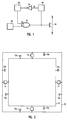
- Figure 1 is a logic diagram illustrating the present invention.
- Figure 2 is a plan view of metal ring layout on an integrated circuit chip.
- Figure 3 is a circuit schematic illustrating the human body model for electrostatic discharge.
- Figure 4 is a plot of current versus time for the circuit of Figure 3.
- Figure 5 is a circuit schematic of a detection and control circuit in accordance with the present invention.
- a circuit for detecting and controlling a pulse of electrostatic discharge ("ESD") which impinges on an IC chip package.
- ESD electrostatic discharge
- the ESD pulse may appear across any pair of pins on the IC package.
- the present invention includes a plurality of RC networks which are designed to provide time constants which are comparable to different characteristics of the ESD pulse waveform, including pulse rise time and pulse duration, so as to provide a logic circuit for controlling the switching element.
- a generalized block diagram of the present invention is illustrated in Figure 1.
- a two input NAND gate 22 drives the switching element 16.
- the switching element 16 will be on if either input S ⁇ (set) or FB (feedback) is low (logical 0).
- the S ⁇ input is driven by a first RC network 30 which has a first time constant t1 which must be longer than the rise time of the ESD pulse, but shorter than the duration of the ESD pulse and shorter than the rise time of a normal application power supply.
- the FB input is driven by a feedback loop from the output of the NAND gate 22.
- the feedback loop includes a second RC network 40 and a third RC network 50 with an inverter 24 between them.
- the inverter input R ⁇ is driven by the second RC network 40 which has a second time constant t2.
- the second time constant t2 is designed to confirm that an ESD pulse of expected duration has been detected, and not a false signal such as a rapid power up or noise on the power line. If so, then the NAND gate 22 will be latched by the feedback input FB and the switching element will be clamped on for a time period equal to a third time constant t3 of the third RC network 40.
- an IC chip includes at least two metal rings 10, 12 which traverse the periphery of the IC chip in order to carry current and provide reference voltages to the individual integrated circuit features (not shown).
- Metal ring 10 is connected to a high reference voltage, VCC (approximately 5 volts DC), and metal ring 12 connected to is a low reference voltage, VSS (usually ground).
- VCC high reference voltage
- VSS low reference voltage
- Individual integrated circuit features are connected through diodes and/or transistors (not shown) to the metal rings 10, 12 at one of a plurality of bonding pads 10a, 12a. It should be noted that while only four bonding pads are shown attached to each of the metal rings, there may be more or less bonding pads depending on the type of integrated circuit and its layout.
- the metal rings 10, 12 drop a finite and calculable amount of voltage during an ESD event.
- 3 x 100 mil metal rings are fabricated with the IC to carry current to the various IC features, and the cross-section of such a metal ring will drop 2 volts at 2 amps.
- a plurality of ESD detection and control circuits 14 are connected between the metal rings 10, 12 to detect and control an ESD pulse, such as that illustrated in Figure 4, which may impinge upon any of the bonding pads 10a, 12a.
- a circuit can be constructed to represent the ESD pulse which is issued by the human body.
- a 120 picofarad capacitor C stores up to 3 kilovolts of DC charge, and upon the touching any two bonding pads 10a, 12a, the charge is dissipated through a 5 microhenry inductor L and a 1.5 kiloohm resistor R.
- the ESD pulse waveform from the human body model is illustrated in Figure 4.
- Two of the characteristics of the ESD pulse waveform which are utilized to build the detection and control circuit of the present invention are pulse rise time PR and pulse width or duration PW.
- the pulse rise time PR is typically defined as the time required for the leading edge of the pulse to rise from zero to 90% of its maximum amplitude.
- the pulse width PW is total duration of the pulse, which may be determined by adding the rise time to the decay time, i.e., the time for the signal to decay from its maximum amplitude to 10% of maximum.
- the pulse width PW is approximately 422 nanoseconds.
- the rise time of a actual ESD pulse may actually be as fast as 1 nanosecond or as long as 20 nanoseconds. Further, the duration of a actual ESD pulse may be anywhere from 100 to 1000 nanoseconds.
- a MOS transistor 16 is used as the switching device or ESD clamp by having its drain 16a and source 16b connected between VCC, i.e. metal ring 10, and VSS, i.e., metal ring 12.
- Gate 16c is driven by a NAND gate 22 in the ESD detection and control circuit 20.
- the ESD clamp 16 is an n-channel MOS transistor measuring 6300 microns wide by 1.1 microns long.
- the first input S ⁇ of the NAND gate 22 is driven by the first RC network 30.
- the first RC network 30 includes a resistor 32 connected between VCC and node 34, and a capacitor 36 connected between node 34 and VSS.
- Node 34 is the NAND gate input S ⁇ .
- the RC time constant t1 of the first RC network 30 must be designed to be longer thar the ESD rise time, but much shorter than the ESD duration to allow fast (approximately 100 nanoseconds) VCC power up during normal applications operations. Selecting resistor 32 as 7 kiloohms and capacitor 36 as 5 picofarads yields a 35 nanosecond time constant t1 during which the voltage at node 34 will ramp up during the ESD event.
- the second input FB of the NAND gate 22 is a feedback loop which includes the second RC network 40, the third RC network 50, and an inverter 24 between the second and third RC networks.
- the second RC network 40 has a resistor 42 connected between the NAND output (node 44) and the input R ⁇ to the inverter 24 (node 48) and a capacitor 46 connected between VSS and the node 48.
- the third RC network 50 includes a resistor 52 connected between VCC and node 54 and a capacitor 56 connected between node 54 and the output of the inverter 24.
- Node 54 is the second NAND gate input FB.
- the time constant t2 of the second RC network 40 is intended to ensure that a false trigger of the ESD clamp is not latched.
- a false ESD signal could occur for a rapid power up (less than 5 nanoseconds) of the power supply, caused by system operating noise which exceeds a few volts.
- the time constant t3 of the third RC network 50 is designed to maintain the latch on the NAND gate 22 for the duration of the ESD pulse, provided that the ESD pulse duration exceeded time constant t2. This can be done by selecting resistor 52 to be 1 megohm and capacitor 56 to be 2 picofarads. This yields a time constant t3 of 2 microseconds.
- the NAND gate 22 preferably consists of a pair of CMOS transistors for the S ⁇ input and the FB input, respectively.
- the S ⁇ input CMOS measures 800 microns wide by 1.1 microns long in its p-channel and 1000 microns wide by 1.1 microns long in its n-channel, and has a trip point of VCC/3.
- the FB input CMOS measures 200 microns wide by 1.1 microns long in its p-channel and 1000 microns wide by 1.1 microns long in its n-channel, and has a trip point slightly above the threshold voltage of its n-channel
- the inverter 24 is also a CMOS transistor measuring 60 microns wide by 1.1 microns long in its p-channel and 10 microns wide by 1.1 microns long in its n-channel.
- the trip point is 2*VCC/3.
- the preferred embodiment of the present invention (as shown in Figure 5) has been layed out using 1 micron minimum CMOS geometries in a chip area of 110 square mils (11 mil wide by 10 mil high).
- VCC 0 volts and the ESD clamp 16 if off.
- VCC is driven to 5 volts within a few nanoseconds, and capacitors 36 and 46 begin to charge.
- the clamp 16 is turned on virtually immediately as the voltage between VCC and node 34 rises past the p-channel threshold voltage V tp of the 800 by 1.1 microns p-channel S ⁇ CMOS transistor. However, S ⁇ stays below the VCC/3 trip point of the NAND gate for approximately 18 nanoseconds.
- VCC falls only slightly during the next 50 nanoseconds.
- the feedback path through resistor 42 begins charging capacitor 46 as soon as the clamp 16 is turned on.
- R ⁇ rises above the 2*VCC/3 trip point of the inverter and begins to latch the clamp on.
- VCC then falls fast (to 1.5 volts in 300 nanoseconds) and prevents resistor 52 from charging capacitor 56 above the threshold voltage V tnt of the second NAND input FB. Therefore, as VCC falls due to the clamp 16 being on, node 44 is kept charged to 0.5 volts (a forward-diode drop) above VCC so that the VCC voltage can discharge to about 0.3 volts.
Landscapes
- Engineering & Computer Science (AREA)
- Microelectronics & Electronic Packaging (AREA)
- Physics & Mathematics (AREA)
- Nonlinear Science (AREA)
- Semiconductor Integrated Circuits (AREA)
- Elimination Of Static Electricity (AREA)
- Electrotherapy Devices (AREA)
- Metal-Oxide And Bipolar Metal-Oxide Semiconductor Integrated Circuits (AREA)
Applications Claiming Priority (2)
| Application Number | Priority Date | Filing Date | Title |
|---|---|---|---|
| US07/752,036 US5255146A (en) | 1991-08-29 | 1991-08-29 | Electrostatic discharge detection and clamp control circuit |
| US752036 | 1991-08-29 |
Publications (1)
| Publication Number | Publication Date |
|---|---|
| EP0533336A1 true EP0533336A1 (de) | 1993-03-24 |
Family
ID=25024578
Family Applications (1)
| Application Number | Title | Priority Date | Filing Date |
|---|---|---|---|
| EP92307160A Withdrawn EP0533336A1 (de) | 1991-08-29 | 1992-08-05 | Elektrostatische Entladungsdetektion und Klemm-Steuerschaltung |
Country Status (4)
| Country | Link |
|---|---|
| US (1) | US5255146A (de) |
| EP (1) | EP0533336A1 (de) |
| JP (1) | JPH05235274A (de) |
| KR (1) | KR930005351A (de) |
Cited By (7)
| Publication number | Priority date | Publication date | Assignee | Title |
|---|---|---|---|---|
| WO2003069673A1 (fr) * | 2002-02-13 | 2003-08-21 | Allied Telesis Kabushiki Kaisha | Circuit de suppression de defaillances pour dispositif a semi-conducteurs |
| WO2009085363A3 (en) * | 2007-10-05 | 2009-09-03 | Arizona Board Of Regents For And On Behalf Of Arizona State University | Ic disabling circuit |
| EP1921900A3 (de) * | 2006-11-09 | 2011-04-06 | Patent-Treuhand-Gesellschaft für elektrische Glühlampen mbH | Beleuchtungsvorrichtung mit einer Lichtquelle und einer Tastvorrichtung |
| EP2567435A4 (de) * | 2010-05-03 | 2013-10-23 | Freescale Semiconductor Inc | Überspannungsschutzschaltung für einen integrierten schaltkreis |
| CN103427826A (zh) * | 2012-05-03 | 2013-12-04 | 联发科技股份有限公司 | 输出电路 |
| CN108254644A (zh) * | 2018-02-08 | 2018-07-06 | 芯颖科技有限公司 | Esd检测装置、系统及方法 |
| CN110907727A (zh) * | 2019-11-25 | 2020-03-24 | 伯恩光学(惠州)有限公司 | 一种esd防护用品的检测系统及方法 |
Families Citing this family (56)
| Publication number | Priority date | Publication date | Assignee | Title |
|---|---|---|---|---|
| US5361185A (en) * | 1993-02-19 | 1994-11-01 | Advanced Micro Devices, Inc. | Distributed VCC/VSS ESD clamp structure |
| US5508649A (en) * | 1994-07-21 | 1996-04-16 | National Semiconductor Corporation | Voltage level triggered ESD protection circuit |
| US5559659A (en) * | 1995-03-23 | 1996-09-24 | Lucent Technologies Inc. | Enhanced RC coupled electrostatic discharge protection |
| US5745323A (en) * | 1995-06-30 | 1998-04-28 | Analog Devices, Inc. | Electrostatic discharge protection circuit for protecting CMOS transistors on integrated circuit processes |
| US5825603A (en) * | 1995-12-21 | 1998-10-20 | Intel Corporaiton | Method and apparatus for providing electrostatic discharge protection for high voltage inputs |
| US6609928B1 (en) | 1996-06-14 | 2003-08-26 | Intel Corporation | Stack universal serial bus connector |
| US5744842A (en) * | 1996-08-15 | 1998-04-28 | Industrial Technology Research Institute | Area-efficient VDD-to-VSS ESD protection circuit |
| US5877927A (en) * | 1996-10-01 | 1999-03-02 | Intel Corporation | Method and apparatus for providing electrostatic discharge protection for high voltage inputs |
| US6008684A (en) * | 1996-10-23 | 1999-12-28 | Industrial Technology Research Institute | CMOS output buffer with CMOS-controlled lateral SCR devices |
| US5838146A (en) * | 1996-11-12 | 1998-11-17 | Analog Devices, Inc. | Method and apparatus for providing ESD/EOS protection for IC power supply pins |
| US5910873A (en) * | 1997-02-19 | 1999-06-08 | National Semiconductor Corporation | Field oxide transistor based feedback circuit for electrical overstress protection |
| US6211554B1 (en) * | 1998-12-08 | 2001-04-03 | Littelfuse, Inc. | Protection of an integrated circuit with voltage variable materials |
| JP2001060663A (ja) * | 1999-08-20 | 2001-03-06 | Nec Corp | 半導体集積回路装置 |
| US6249410B1 (en) | 1999-08-23 | 2001-06-19 | Taiwan Semiconductor Manufacturing Company | ESD protection circuit without overstress gate-driven effect |
| US6912109B1 (en) | 2000-06-26 | 2005-06-28 | Taiwan Semiconductor Manufacturing Co., Ltd. | Power-rail ESD clamp circuits with well-triggered PMOS |
| US6552886B1 (en) | 2000-06-29 | 2003-04-22 | Pericom Semiconductor Corp. | Active Vcc-to-Vss ESD clamp with hystersis for low supply chips |
| US6624992B1 (en) * | 2000-10-06 | 2003-09-23 | Qualcomm, Incorporated | Electro-static discharge protection circuit |
| US6690555B1 (en) * | 2001-03-25 | 2004-02-10 | National Semiconductor Corporation | Electrostatic discharge protection circuit with cascoded trigger-switch suitable for use with over-voltage tolerant CMOS input/output buffers |
| JP2002305254A (ja) * | 2001-04-05 | 2002-10-18 | Mitsubishi Electric Corp | 半導体装置およびその製造方法 |
| US6801416B2 (en) * | 2001-08-23 | 2004-10-05 | Institute Of Microelectronics | ESD protection system for high frequency applications |
| US7164565B2 (en) * | 2002-11-29 | 2007-01-16 | Sigmatel, Inc. | ESD protection circuit |
| US7187530B2 (en) | 2002-12-27 | 2007-03-06 | T-Ram Semiconductor, Inc. | Electrostatic discharge protection circuit |
| US7224560B2 (en) * | 2003-02-13 | 2007-05-29 | Medtronic, Inc. | Destructive electrical transient protection |
| US7304827B2 (en) * | 2003-05-02 | 2007-12-04 | Zi-Ping Chen | ESD protection circuits for mixed-voltage buffers |
| US6989979B1 (en) | 2003-09-22 | 2006-01-24 | Pericom Semiconductor Corp. | Active ESD shunt with transistor feedback to reduce latch-up susceptibility |
| US7129589B2 (en) * | 2003-10-22 | 2006-10-31 | Broadcom Corporation | Use of an internal on-chip inductor for electrostatic discharge protection of circuits which use bond wire inductance as their load |
| US7292421B2 (en) * | 2004-11-12 | 2007-11-06 | Texas Instruments Incorporated | Local ESD power rail clamp which implements switchable I/O decoupling capacitance function |
| JP4647294B2 (ja) * | 2004-11-26 | 2011-03-09 | ルネサスエレクトロニクス株式会社 | 半導体装置 |
| TWI258071B (en) * | 2004-12-13 | 2006-07-11 | Via Tech Inc | Mainboard and power control device thereof |
| JP4504850B2 (ja) * | 2005-03-17 | 2010-07-14 | パナソニック株式会社 | 半導体集積回路装置 |
| US7301741B2 (en) * | 2005-05-17 | 2007-11-27 | Freescale Semiconductor, Inc. | Integrated circuit with multiple independent gate field effect transistor (MIGFET) rail clamp circuit |
| KR100990466B1 (ko) | 2005-10-14 | 2010-10-29 | 리서치 인 모션 리미티드 | 모바일 장치용 배터리 팩 인증 |
| EP2287993B1 (de) * | 2005-10-14 | 2018-03-28 | BlackBerry Limited | Kommunikationsverfahren für intelligentes Batteriesystem |
| US7715884B2 (en) * | 2005-10-14 | 2010-05-11 | Research In Motion Limited | Mobile device with a smart battery having a battery information profile corresponding to a communication standard |
| US7593202B2 (en) * | 2005-11-01 | 2009-09-22 | Freescale Semiconductor, Inc. | Electrostatic discharge (ESD) protection circuit for multiple power domain integrated circuit |
| US7453676B2 (en) * | 2005-11-16 | 2008-11-18 | Huh Yoon J | RC-triggered ESD power clamp circuit and method for providing ESD protection |
| CN100544205C (zh) * | 2005-12-07 | 2009-09-23 | 群康科技(深圳)有限公司 | 防治静电放电导致电子装置复位的方法 |
| TWI300291B (en) * | 2006-03-16 | 2008-08-21 | Novatek Microelectronics Corp | Logic-latching apparatus for improving system-level electrostatic discharge robustness |
| WO2007124079A2 (en) * | 2006-04-21 | 2007-11-01 | Sarnoff Corporation | Esd clamp control by detection of power state |
| TW200742223A (en) * | 2006-04-26 | 2007-11-01 | Novatek Microelectronics Corp | Logic-keeping apparatus for improving system-level electrostatic discharge robustness |
| US7589945B2 (en) * | 2006-08-31 | 2009-09-15 | Freescale Semiconductor, Inc. | Distributed electrostatic discharge protection circuit with varying clamp size |
| US7929263B1 (en) * | 2007-08-01 | 2011-04-19 | Rf Micro Devices, Inc. | Unlatch feature for latching ESD protection circuit |
| US7868620B2 (en) * | 2007-08-29 | 2011-01-11 | Seagate Technology Llc | Data integrity management responsive to an electrostatic event |
| US7777998B2 (en) | 2007-09-10 | 2010-08-17 | Freescale Semiconductor, Inc. | Electrostatic discharge circuit and method therefor |
| US7817387B2 (en) * | 2008-01-09 | 2010-10-19 | Freescale Semiconductor, Inc. | MIGFET circuit with ESD protection |
| US7826187B2 (en) * | 2008-04-23 | 2010-11-02 | Himax Technologies Limited | Transient detection circuit |
| US8116047B2 (en) * | 2008-12-18 | 2012-02-14 | Sandisk Technologies Inc. | Electrostatic discharge protective circuit having rise time detector and discharge sustaining circuitry |
| US8514533B2 (en) * | 2010-06-24 | 2013-08-20 | Intel Corporation | Method, apparatus, and system for protecting supply nodes from electrostatic discharge |
| US9013842B2 (en) | 2011-01-10 | 2015-04-21 | Infineon Technologies Ag | Semiconductor ESD circuit and method |
| US8413101B2 (en) | 2011-07-15 | 2013-04-02 | Infineon Technologies Ag | System and method for detecting parasitic thyristors in an integrated circuit |
| DE102011109596B4 (de) * | 2011-08-05 | 2018-05-09 | Austriamicrosystems Ag | Schaltungsanordnung zum Schutz gegen elektrostatische Entladungen |
| US9438030B2 (en) | 2012-11-20 | 2016-09-06 | Freescale Semiconductor, Inc. | Trigger circuit and method for improved transient immunity |
| US9679891B2 (en) * | 2014-03-20 | 2017-06-13 | Apple Inc. | Optimized ESD clamp circuitry |
| US9608429B2 (en) * | 2014-03-27 | 2017-03-28 | Texas Instruments Incorporated | Logging ESD events |
| EP3246784B1 (de) | 2016-05-19 | 2020-01-01 | NXP USA, Inc. | Kompensationsschaltung |
| US10826291B2 (en) | 2018-09-12 | 2020-11-03 | CoolStar Technology, Inc. | Electrostatic discharge transient power clamp |
Family Cites Families (4)
| Publication number | Priority date | Publication date | Assignee | Title |
|---|---|---|---|---|
| US4363068A (en) * | 1980-08-18 | 1982-12-07 | Sundstrand Corporation | Power FET short circuit protection |
| JPS6150358A (ja) * | 1984-08-20 | 1986-03-12 | Toshiba Corp | 半導体集積回路 |
| JPH0683042B2 (ja) * | 1986-03-31 | 1994-10-19 | 株式会社東芝 | 出力ドライバ回路 |
| FR2623018B1 (fr) * | 1987-11-06 | 1990-02-09 | Thomson Semiconducteurs | Circuit integre protege contre les decharges electrostatiques avec seuil de protection variable |
-
1991
- 1991-08-29 US US07/752,036 patent/US5255146A/en not_active Expired - Lifetime
-
1992
- 1992-08-05 EP EP92307160A patent/EP0533336A1/de not_active Withdrawn
- 1992-08-28 KR KR1019920015563A patent/KR930005351A/ko not_active Withdrawn
- 1992-08-28 JP JP4229576A patent/JPH05235274A/ja active Pending
Non-Patent Citations (1)
| Title |
|---|
| PATENT ABSTRACTS OF JAPAN, vol. 14, no. 200 (E-920)(4143), 24th April 1990; & JP-A-2 41 621 (MATSUSHITA ELECTRON CORP.) 09-02-1990 * |
Cited By (11)
| Publication number | Priority date | Publication date | Assignee | Title |
|---|---|---|---|---|
| WO2003069673A1 (fr) * | 2002-02-13 | 2003-08-21 | Allied Telesis Kabushiki Kaisha | Circuit de suppression de defaillances pour dispositif a semi-conducteurs |
| US6621297B2 (en) | 2002-02-13 | 2003-09-16 | Allied Telesis K.K. | Semiconductor device malfunction preventive circuit |
| EP1921900A3 (de) * | 2006-11-09 | 2011-04-06 | Patent-Treuhand-Gesellschaft für elektrische Glühlampen mbH | Beleuchtungsvorrichtung mit einer Lichtquelle und einer Tastvorrichtung |
| WO2009085363A3 (en) * | 2007-10-05 | 2009-09-03 | Arizona Board Of Regents For And On Behalf Of Arizona State University | Ic disabling circuit |
| EP2567435A4 (de) * | 2010-05-03 | 2013-10-23 | Freescale Semiconductor Inc | Überspannungsschutzschaltung für einen integrierten schaltkreis |
| CN103427826A (zh) * | 2012-05-03 | 2013-12-04 | 联发科技股份有限公司 | 输出电路 |
| US9263882B2 (en) | 2012-05-03 | 2016-02-16 | Mediatek Inc. | Output circuits with electrostatic discharge protection |
| CN103427826B (zh) * | 2012-05-03 | 2016-06-08 | 联发科技股份有限公司 | 输出电路 |
| CN108254644A (zh) * | 2018-02-08 | 2018-07-06 | 芯颖科技有限公司 | Esd检测装置、系统及方法 |
| CN108254644B (zh) * | 2018-02-08 | 2020-06-26 | 芯颖科技有限公司 | Esd检测装置、系统及方法 |
| CN110907727A (zh) * | 2019-11-25 | 2020-03-24 | 伯恩光学(惠州)有限公司 | 一种esd防护用品的检测系统及方法 |
Also Published As
| Publication number | Publication date |
|---|---|
| JPH05235274A (ja) | 1993-09-10 |
| US5255146A (en) | 1993-10-19 |
| KR930005351A (ko) | 1993-03-23 |
Similar Documents
| Publication | Publication Date | Title |
|---|---|---|
| US5255146A (en) | Electrostatic discharge detection and clamp control circuit | |
| US7245468B2 (en) | Electro-static discharge (ESD) power clamp with power up detection | |
| US5978192A (en) | Schmitt trigger-configured ESD protection circuit | |
| US5239440A (en) | Electrostatic discharge protection for integrated circuits | |
| US8116047B2 (en) | Electrostatic discharge protective circuit having rise time detector and discharge sustaining circuitry | |
| US5959820A (en) | Cascode LVTSCR and ESD protection circuit | |
| EP0740344B1 (de) | Verfahren und Apparat zum Koppeln verschiedener, unabhängiger on-Chip-Vdd-Busse an eine ESD-Klemme | |
| US5835328A (en) | Breakdown-tiggered transient discharge circuit | |
| US7457086B2 (en) | High voltage ESD power clamp | |
| US6756834B1 (en) | Direct power-to-ground ESD protection with an electrostatic common-discharge line | |
| US6552886B1 (en) | Active Vcc-to-Vss ESD clamp with hystersis for low supply chips | |
| US7738222B2 (en) | Circuit arrangement and method for protecting an integrated semiconductor circuit | |
| US5917689A (en) | General purpose EOS/ESD protection circuit for bipolar-CMOS and CMOS integrated circuits | |
| US6118640A (en) | Actively-driven thin-oxide MOS transistor shunt for ESD protection of multiple independent supply busses in a mixed-signal chip | |
| US6624998B2 (en) | Electrostatic discharge protection scheme in low potential drop environments | |
| CN100508322C (zh) | 用于集成电路器件的保护电路 | |
| EP0730347A2 (de) | Halbleitervorrichtung | |
| US5644460A (en) | Multi-rail electrostatic discharge protection device | |
| US5825603A (en) | Method and apparatus for providing electrostatic discharge protection for high voltage inputs | |
| US6621679B1 (en) | 5V tolerant corner clamp with keep off circuit | |
| US5910873A (en) | Field oxide transistor based feedback circuit for electrical overstress protection | |
| US5521789A (en) | BICMOS electrostatic discharge protection circuit | |
| KR100587089B1 (ko) | 반도체 장치용 정전기 보호장치 | |
| CN114303309B (zh) | 过流保护电路及开关电路 | |
| US5285346A (en) | Current driven control circuit for a power device |
Legal Events
| Date | Code | Title | Description |
|---|---|---|---|
| PUAI | Public reference made under article 153(3) epc to a published international application that has entered the european phase |
Free format text: ORIGINAL CODE: 0009012 |
|
| AK | Designated contracting states |
Kind code of ref document: A1 Designated state(s): DE FR GB IT |
|
| 17P | Request for examination filed |
Effective date: 19930916 |
|
| 17Q | First examination report despatched |
Effective date: 19941128 |
|
| STAA | Information on the status of an ep patent application or granted ep patent |
Free format text: STATUS: THE APPLICATION IS DEEMED TO BE WITHDRAWN |
|
| 18D | Application deemed to be withdrawn |
Effective date: 19950609 |