EP0532021B1 - Coherent subcarrier multiplexed optical communication system - Google Patents
Coherent subcarrier multiplexed optical communication system Download PDFInfo
- Publication number
- EP0532021B1 EP0532021B1 EP92115569A EP92115569A EP0532021B1 EP 0532021 B1 EP0532021 B1 EP 0532021B1 EP 92115569 A EP92115569 A EP 92115569A EP 92115569 A EP92115569 A EP 92115569A EP 0532021 B1 EP0532021 B1 EP 0532021B1
- Authority
- EP
- European Patent Office
- Prior art keywords
- light
- signal
- frequency
- unmodulated
- communication system
- Prior art date
- Legal status (The legal status is an assumption and is not a legal conclusion. Google has not performed a legal analysis and makes no representation as to the accuracy of the status listed.)
- Expired - Lifetime
Links
Images


Classifications
-
- H—ELECTRICITY
- H04—ELECTRIC COMMUNICATION TECHNIQUE
- H04J—MULTIPLEX COMMUNICATION
- H04J14/00—Optical multiplex systems
- H04J14/02—Wavelength-division multiplex systems
- H04J14/0298—Wavelength-division multiplex systems with sub-carrier multiplexing [SCM]
Definitions
- the present invention relates to an optical communication system for performing communication according to data signals by modulating and transmitting optics, and specifically to a phase noise cancelling system for reducing phase noise in an optical communication system comprising a phase processing unit.
- Optical communication systems have made a remarkable progress with the development of coherent optical communication systems.
- the amplitude, frequency, and phase, etc. of a high-coherency laser light emitted from a light source such as semiconductor lasers, etc. are modulated in the sending equipment directly by a data signal to be communicated.
- Resultant modulated light is transmitted through a low-loss, broadband, and nonconductive transmission line such as optical fiber cables.
- received modulated light is converted by optical heterodyne detection or homodyne detection into an electric signal having a frequency in an intermediate frequency band or a base band frequency band, and a data signal is demodulated from the electric signal.
- laser light that is, carrier light
- the data signal is thus transmitted as a modulation component of carrier light, and can be received with high sensitivity through optical heterodyne or homodyne detection.
- a large light frequency range (light wavelength range) can be used through the optical heterodyne detection, etc.
- a multiplexed light frequency (wavelength) transmission system for transmitting a data signal of a plurality of channels can be realized using various light carriers having different frequencies (wavelengths).
- the applicant of the present application refers to a subcarrier multiplexing (SCM) optical communication system in the patent application of "Tokugan-hei P2-242615" in Japan and in the US Patent Application having serial number "07/760,019".
- SCM optical communication system a data signal of a plurality of channels is frequency- multiplexed at a microwave level in an electrical stage, and the resultant electric signal modulates carrier light.
- a frequency multiplexing operation is not always required in a light stage, but an electrical stage multiplexes a frequency (in sending equipment) or identifies it (in receiving equipment).
- an electrical stage multiplexes a frequency (in sending equipment) or identifies it (in receiving equipment).
- the above described SCM optical communication system can be combined with a coherent optical communication system using direct modulation of the above described semiconductor laser light, etc. and optical heterodyne detection, etc.
- a coherent optical communication system using direct modulation of the above described semiconductor laser light, etc. and optical heterodyne detection, etc.
- an optical communication system having a higher channel density and a larger capacity than a conventional coherent optical communication system and a conventional SCM optical communication system can be realized at a low cost.
- the latest optical communication system such as coherent optical communication systems, SCM optical communication systems, and coherent SCM optical communication systems, etc. can be widely used for various applications in a conventional optical communication system, a broadband transmission system for an optical CATV (Cable Television) network and image information, and in any large capacity optical communication network for the future ISDN (Integrated Service Digital Network), etc.
- a conventional optical communication system a broadband transmission system for an optical CATV (Cable Television) network and image information
- ISDN Integrated Service Digital Network
- phase noise In the above described various optical communication systems, if the frequency or the phase of a carrier light can be modulated by a data signal, random phase noise of the carrier itself or phase noise incorporated in the communication process greatly affect the demodulating function of the data signal. Therefore, such phase noise must be appropriately cancelled.
- phase noise affects the demodulating function of a data signal if optical heterodyne detection is performed in the demodulating process and a data signal is transmitted at a low rate.
- the phase noise cancelling method can be a light frequency canceling method or an intermediate frequency stage (IF stage) canceling method after optical heterodyne (or optical homodyne) detection.
- IF stage intermediate frequency stage
- the phase noise cancelling method in the light stage the light circuit is complicated, and the center frequency of modulated light is much higher (about 1000 times) than the center frequency in the IF stage-after the detection, thereby requiring precise control and hardly guaranteeing its realization.
- the phase noise cancelling process can be realized in the IF stage much more easily.
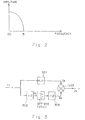
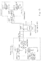
- Figure 1 shows a basic configuration of the conventional coherent optical communication system capable of cancelling phase noise.
- Data signal D is a communication signal in the base band having a predetermined transmission rate B.
- Figure 2 shows its frequency characteristics. Data signal D requires that the main lobe of its frequency component is securely stored. Therefore, in data signal D, harmonic components other than the main lobe are removed by a low-pass filter.
- a light modulator 101 modulates using data signal D a carrier light having a light frequency of f s .
- the light modulating method is, for example, a phase shift keying (PSK) method.
- the carrier light is, for example, laser light from a semiconductor laser (a distributed feedback (DFB) semiconductor laser having a broadband with a narrow width of a spectral line is desirable).
- DFB distributed feedback
- the above described light modulating operation can be realized as directly modulating using data signal D the bias voltage of the LiNbO 3 light phase modulator and the bias current or temperature of the semiconductor laser.
- Modulated light obtained by the light modulator 101 is transmitted through optical fibers 102.
- Modulated light transmitted through the optical fiber 102 is mixed in a mixing circuit 103 with a local oscillator light beam having a center frequency of f L from a local oscillator laser divice (Lo-LD) 104 which is a semiconductor laser.
- the mixed light is optical-heterodyne-detected by being received by a light detector 105 such as photodiodes.
- between the center light frequency f s of the modulated light (equal to the center light frequency of the carrier light) and the light frequency f L of the local oscillator light equals the center frequency f if of an electric signal in the intermediate frequency stage (IF stage) after the detection.
- the mixing circuit 103 can be, for example, a half-nirror or fiber-type light coupler.
- An intermediate frequency signal output by the light detector 105 is amplified by an amplifier 106, and then applied to a phase noise cancelling circuit (PNC) 107 where phase noise contained in an intermediate frequency signal is cancelled.
- PNC phase noise cancelling circuit
- the intermediate frequency signal in which phase noise is cancelled can be demodulated by a demodulating circuit (DEMOD) 108.
- DEMOD demodulating circuit
- FIG 3 shows the configuration of the PNC 107 shown in Figure 1.
- a carrier component is regenerated from a received intermediate frequency signal. Then, phase noise can be cancelled by comparing the phase between the carrier component and the received intermediate frequency signal.
- a data signal in a base band is transmitted as a modulated component of a carrier light as described above. Therefore, in the IF stage after the detection, the band of the frequency f if of a carrier component and the frequency band of a data signal are included. Accordingly, only the carrier component must be regenerated by appropriate means.
- a received intermediate frequency signal is branched to two routes.
- a received intermediate frequency signal is delayed by a delay circuit 301.
- a carrier component is regenerated by a frequency multiplier 302, a band-pass filter 303, and a frequency divider 304.
- an output signal in each route is mixed by a multiplier 305, thereby generating a demodulated signal with phase noise cancelled.
- phase noise cancelling method based on the configuration shown in Figure 3 is explained below.
- the configuration shown in Figure 3 can be assumed if the light modulator 101 shown in Figure 1 light-modulates a data signal D, which is a digital signal, by the PSK method.
- D which is a digital signal
- a 1 - A 5 are predetermined constants.
- the intermediate frequency signal I 1 applied from the amplifier 106 shown in Figure 1 can be represented by the following equation (1).
- I 1 A 1 cos ⁇ 2 ⁇ f if t + ⁇ (t) + ⁇ (t) ⁇ where ⁇ (t) indicates a phase component corresponding to a data signal D light-modulated by the PSK method, and has a phase value of either 0 or ⁇ .
- ⁇ (t) indicates phase noise to be cancelled.
- the intermediate frequency signal I 1 is branched to two routes.
- an intermediate frequency signal I 2 delayed by the delay circuit 301 in the first route can be represented by the following equation (2) according to equation (1).
- I 2 A 1 cos ⁇ 2 ⁇ f if (t - ⁇ t 1 ) + ⁇ (t - ⁇ t 1 ) + ⁇ (t - ⁇ t 1 ) ⁇ where ⁇ t 1 indicates a delay time in the delay circuit 301.
- An intermediate frequency signal I 3 having the frequency doubled by the frequency multiplier 302 in the second route can be represented by the following equation according to equation (1).
- I 3 A 2 cos ⁇ 2 ⁇ 2f if t + 2 ⁇ (t) ⁇
- the intermediate frequency signal I 3 is filtered through the band-pass filter (BPF) 303 for passing only the frequency components close to the frequency 2f if' and then applied to the frequency divider 304.
- An intermediate frequency signal I 4 output by the frequency divider 304 can be represented by the following equation according to equation (3) above.
- I 4 A 3 cos ⁇ 2 ⁇ f if t + ⁇ (t) ⁇ where a time delay arises when an intermediate frequency signal is transmitted through the frequency multiplier 302, the BPF 303, and the frequency divider 304.
- an output I 4 of the frequency divider 304 can be represented by the following equation (4) according to the equation above, where ⁇ t 2 indicates the time delay.
- I 4 A 3 cos ⁇ 2 ⁇ f if (t - ⁇ t 2 ) + ⁇ (t - ⁇ t 2 ) ⁇
- an intermediate frequency signal I 4 which is a carrier component, can be regenerated from the second route.
- a component I 5 in the detection band can be represented by the following equation (5) according to the above equations 2 and 4.
- I 5 A 4 cos ⁇ 2 ⁇ f if ( ⁇ t 1 - ⁇ t 2 ) - ⁇ (t - ⁇ t 1 ) - ⁇ ( ⁇ t 1 - ⁇ t 2 ) ⁇
- ⁇ ( ⁇ t 1 - ⁇ t 2 ) indicates phase noise contained in the output from the multiplier 305, and can be represented by the following equation (6).
- ⁇ ( ⁇ t 1 - ⁇ t 2 ) ⁇ (t - ⁇ t 1 ) - ⁇ (t - ⁇ t 2 )
- phase noise indicates zero-mean Gaussian white noise
- ⁇ 2 the variance of the phase deviation can be represented by the following equation (7).
- ⁇ 2 2 ⁇ if ⁇ t 1 - ⁇ t 2 where ⁇ if indicates the line width of a beat spectrum.
- the fluctuation of the phase noise component ⁇ ( ⁇ t 1 - ⁇ t 2 ) can be set to 0 by controlling the delay circuit 301 such that the time delay ⁇ t 1 in the delay circuit 301 equals the time delay ⁇ t 2 in the frequency multiplier 302, the BPF 303, and the frequency divider 304.
- the output I 5 from the multiplier 305 represented in the above described equation (5) is represented in the following equation (8).
- I 5 A 4 cos ⁇ (t - ⁇ t 1 ) ⁇ where the phase noise is cancelled out.
- the conventional coherent optical communication system having the configuration shown in Figures 1 and 3 requires in the configuration of the PNC 107 the frequency multiplier 302, the BPF 303, and the frequency divider 304, etc. in order to regenerate a carrier component from a received intermediate frequency signal. This offers the problem that the total cost of the system rises considerably.
- the light phase modulation (0, ⁇ ) must be successfully performed. This is accompanied by the problem of difficulty in techniques.
- Figure 4 shows the basic configuration of the conventional coherent SCM optical communication system capable of canceling phase noises.
- the sending equipment is explained below.
- Each of modulators 401-1 - 401-N modulates each of the carriers of the different frequencies f 1 - f N allocated to each channel according to each of the data signals D 1 - D N .
- This modulating method can be an amplitude modulation (AM), a frequency modulation (FM), or a phase modulation (PM) if the data signal D is an analog signal, and can be an amplitude shift keying (ASK), a frequency shift keying (FSK), or a phase shift keying (PSK) if the data signal D is a digital signal.
- a multiplexer 402 composes each of the channel signals modulated by each of the modulators 401-1 - 401-N to generate a subcarrier multiplexed signal (an SCM signal).
- the multiplexer 402 only has to be equipped with a function of adding electric signals, and can be realized from a simple and cheap unit such as a micro-wave coupler, etc.
- Each of the channel signals must be frequency-multiplexed in the frequency axis so that signals may not leak to the adjacent channels.
- a band-pass filtering process is performed based on each of the frequencies f i after the modulation such that only the signal component of the main lobe of each data signal D i can be extracted. That is, if the transmission rate of a data signal D i is defined as B i , a band-pass filtering process is performed, where the cut-off frequency is f i ⁇ B i after the modulation.
- a low-pass filtering process in which a cut-off frequency is defined as B i can be performed before the modulation such that only the signal component of the main lobe of each data signal D i in the base band can be extracted.
- the frequency interval for each channel signal can be approximately double the data transmission rate B i at minimum for a digital signal.
- Figure 5 shows the configuration of channels on the frequency axis of an SCM signal obtained by the multiplexer 402.
- a light modulator 403 modulates a carrier light having the light frequency of f s according to an SCM signal output by the multiplexer 402.
- This light modulating method can be an AM, an FM, or a PM method.
- the carrier light can be a laser light obtained by a semiconductor laser, etc.
- the modulated light obtained by the light modulator 403 is transmitted through optical fibers 404.
- a modulated light transmitted through the optical fiber 404 is optical-heterodyne-detected by a mixing circuit 405, a Lo-LD 406, and a light detector 407 in the same configuration as that shown in Figure 1.
- the center frequency f if of the intermediate frequency signal obtained by the light detector 407 is equal to the difference frequency
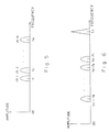
- Figure 6 shows the configuration of the first-order lower side band IF spectrum having the above described center frequency f if .
- each of the subcarrier components having the center frequencies f if - f 1 , f if - f 2 , ..., f if - f N is frequency-multiplied with the unmodulated main carrier component at the frequency f if .
- the above described intermediate frequency signal is applied to the PNC 409 after being amplified by an amplifier 408, and the phase noise contained in the intermediate frequency signal is canceled by a PNC 409.
- the intermediate frequency signal is branched to the number of channels after having the phase noise canceled.
- Each of demodulators 410-1 - 410-N extracts each of the subcarrier components close to each of the center frequencies of f if - f 1 , f if - f 2 , ..., f if -f N from each of the above described branched center frequency signals, and demodulates each of the data signals D 1 - D N .
- a frequency-multiplexed signal (SCM signal) is generated by cheap multiplexers such as microwave couplers in the electric stage, and then, the light modulation is performed by the SCM signal. Therefore, only one light modulator is required, and the total cost for the whole system can be considerably reduced.
- the interval of channels can be approximated to double the transmission rate in the sending equipment. Therefore, the receiving equipment can collectively receive all or a plurality of channels using a broadband receiver.
- Figure 7 shows the configuration of the PNC 409 shown in Figure 4.
- this prior art technology extracts a main carrier component from a received intermediate frequency signal. Then, a phase noise can be canceled by comparing the phase of the main carrier component with that of the intermediate frequency signal.
- a received intermediate frequency signal is branched to two routes.
- the received intermediate frequency signal is delayed by a delay circuit 701.
- the main carrier component is extracted by a band-pass filter 702.
- a multiplier 703 mixes output signals in both routes, and an intermediate frequency signal in which a phase noise is canceled can be obtained.
- phase noise canceling method based on the configuration shown in Figure 7 is explained below.
- the light modulator 403 shown in Figure 4 performs a light modulation in the PM method.
- equations A 6 , A 6 ', A 7 , and A 8 indicate predetermined constants.
- an intermediate frequency signal I 6 applied by the amplifier 408 shown in Figure 4 can be represented by the following equation (9).
- D i (t) (1 ⁇ i ⁇ N) indicates a data signal of each channel
- f if indicates a main carrier frequency in the IF stage
- f i (1 ⁇ i ⁇ N) indicates a carrier frequency in the electric stage corresponding to each channel ( Figure 5)
- (f if - f i ) indicates a subcarrier frequency in the IF stage.
- m indicates a modulation index or an PM modulation index
- ⁇ (t) indicates a phase noise to be canceled
- the intermediate frequency signal I 6 is branched to two routes.
- an intermediate frequency signal I 7 delayed by the delay circuit 701 in the first route can be represented by the following equation (10) according to equation (9).
- ⁇ t 1 indicates delay time in the delay circuit 701 as in the case shown in Figure 3.
- the BPF 702 in the second route only passes the frequency component close to the main carrier frequency f if .
- An output I 8 from the BPF 702 can be represented by the following equation (11), where the time delay is defined as ⁇ t 2 , according to the equation above.
- I 8 A 7 J 0 (m)cos ⁇ 2 ⁇ f if (t - ⁇ t 2 ) + ⁇ (t - ⁇ t 2 ) ⁇
- the intermediate frequency signal I 8 which is a main carrier component, can be regenerated from the second route.
- a component I 9 in the detection band can be represented by the following equation (12) according to equations (10) and (11).
- I 9 A 8 ⁇ cos ⁇ 2 ⁇ f if ( ⁇ t 1 - ⁇ t 2 ) + 2 ⁇ f i (t - ⁇ t 1 ) + D i (t - ⁇ t 1 ) - ⁇ ( ⁇ t 1 - ⁇ t 2 ) ⁇ where ⁇ ( ⁇ t 1 - ⁇ t 2 ) and ⁇ 2 can be obtained in the same manner as in equations (6) and (7) shown in Figure 3.
- the phase noise component ⁇ ( ⁇ t 1 - ⁇ t 2 ) can be set to 0 by controlling the delay circuit 702 such that the delay time ⁇ t 1 in the delay circuit 701 equals the time delay ⁇ t 2 in the BPF 702. Accordingly, the output I 9 from the multiplier 703 shown in equation (12) above can be represented by the following equation (13).
- I 9 A 8 ⁇ cos ⁇ 2 ⁇ f if (t - ⁇ t 1 ) D i (t - ⁇ t 1 ) ⁇
- the PNC 409 extracts the unmodulated main carrier component of the frequency f if as shown in equations (9) through (13) above.
- each of the subcarrier components having the center frequencies f if - f 1 , f if - f 2 , ..., f if - f N must be processed correspondingly.
- the power of the unmodulated main carrier component at the frequency f if shown in Figure 6 is larger than the power of each of the subcarrier components having the center frequencies f if - f 1 , f if - f 2 , ..., f if - f N . That is, the former has a larger value of (J 0 (m)/J 1 (m)) 2 . Therefore, the frequency interval between the frequency f if of the main carrier component and the center frequency f if - f 1 of the first subcarrier component must be sufficiently wide (about several giga Hz). If the frequency interval is not sufficient, a number of high-degree modulation components enter the reception band, thereby badly reducing the reception sensitivity.
- the optical heterodyne detection circuit comprising the mixing circuit 405, the Lo-LD 406, the light receiver 407, and the amplifier 408 requires a broadband circuit for simultaneously receiving the main carrier components and the subcarrier components.
- the total cost for the whole system soars.
- the present invention has been developed based on the above described background and aims at cancelling phase noise using a simple circuit configuration without a broadband detecting circuit in an optical communication system capable of cancelling phase noise.
- an optical communication system for communicating a data signal by modulating and transmitting light, comprising:
- an optical communication system for communicating a data signal by modulating and transmitting light, comprising:
- an optical communication system for communicating a data signal by receiving and demodulating light, comprising light receiving means for detecting modulated light which has been generated by modulating light according to a composed signal generated by using carrier signals modulated according to transmission data signals, and for converting said detected modulated light to an electric signal, characterised by:
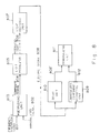
- Figure 8 is a block diagram of the principle of the present invention.
- a coherent subcarrier multiplexing (SCM) optical communication system is applied in the present invention.
- a plurality of electrical stage modulating units (not shown in Figure 8) provided corresponding to each transmission signal in a plurality of channels modulate each carrier signal having a different microwave frequency according to each transmission signal.
- a frequency multiplexing unit (not shown in Figure 8) frequency-multiplexes in the microwave stage each modulated signal from each electric stage modulating unit.
- the frequency-multiplexed signal 801 from the frequency multiplexing unit is applied to the multiplexing unit 803.
- the multiplexing unit 803 multiplexes the above described frequency-multiplexed signal 801 with the unmodulated signal 802 having the frequency out of the frequency band of the frequency-multiplexed signal.
- a light modulating unit 805 performs a light modulation according to a composed signal 804 obtained by the multiplexing unit 803, and outputs a resultant modulated light 806.
- the light modulating method can be an amplitude modulating (AM) method, a frequency modulating (FM) method, or a phase modulating (PM) method.
- the light modulating unit 805 can be made of a semiconductor laser, can contain a LiNb03 modulator or both of them.
- the modulated light 806 is output directly to the light transmission line of optical fibers, etc., or output thereto after mixed with the local oscillator light as described later.
- a light receiving unit 807 detects the modulated light 806 and converts it to an electric signal 808.
- the light receiving unit 807 comprises, for example, a local oscillating unit such as semiconductor lasers, etc. for oscillating, for example, a local oscillator light, a mixing unit for mixing the local oscillator light and the modulated light 806, and a light detecting element such as photodiodes, etc. for detecting the mixed light and converting it to the electric signal 808.
- the configuration can be used for the optical heterodyne detection method if the center frequency of the modulated light is different from the frequency of the local oscillator light, and can be used for the optical homodyne detection method if these frequencies are the same.
- the local oscillating unit and the mixing unit are not necessarily provided in a receiver, but can be provided in a repeater or a transmitter in a light distributing network as described later.
- an unmodulated component extracting unit 809 extracts from the electric signal 808 from the light receiving unit 807 a frequency component 812 of the unmodulated signal 802 multiplexed with the frequency-multiplexed signal 801 in the sending equipment.
- the unmodulated component extractor 809 is a band-pass filter for passing, for example, only the frequency component 812 in the unmodulated signal 802.
- a delay unit 810 delays the electric signal 808' from the light receiving unit 807 by the time equal to the signal delay time in the unmodulated component extracting unit 809.
- a demodulating unit 811 cancels a phase noise based on the phase difference between the electric signal 808 from the delay unit 810 and the frequency component 812 of the unmodulated signal 802 extracted by the unmodulated component extracting unit 809, and demodulates the frequency-multiplexed signal 801.
- a coherent SCM optical communication system is applied to the present invention having the configuration shown in Figure 8.
- plural sets of an electric stage modulating unit, a frequency multiplexing unit, another frequency multiplexing unit 803, and the light modulating unit 805 are provided. It further comprises a light multiplexing unit for multiplexing each of the modulated lights from each of the light modulating units and for outputting a resultant optical frequency multiplexed modulated light as the modulated light 806.
- the present invention having the configuration shown in Figure 8 can be applied to an optical communication system which is a light distributing network.
- the above described local oscillating unit and mixing unit are provided in the repeater in the network.
- the modulated light 806 transmitted through the light transmission line of optical fibers, etc. is branched after being mixed with the local oscillator light by the above described mixing unit in the repeater.
- Each of the branched mixed light beams is received by a plurality of receivers of the above described light receiving element (a part of the light receiving unit 807), the unmodulated component extracting unit 809, the delay unit 810, and the demodulating unit 811.
- a light amplifier can be provided before and/or after the branch in the repeater.
- the present invention can further include a unique countermeasure to polarization.
- the transmitter can comprise not only the above described local oscillating unit and the mixing unit, but also a polarization control unit for controlling the polarization state of the modulated light 806 to be equivalent to the polarization state of the locally oscillator light from the local oscillating unit.
- the modulated light 806 and the local oscillator light are controlled by the polarization control unit to indicate the coincident polarization state, and are mixed by the mixing unit from which the mixed light is transmitted to the receiver through the light transmission line.
- the transmitter can comprise a light amplifier for light-amplifying the mixed light from the mixing unit and transmitting it to the light transmission line.
- the above configuration can be applied to an optical communication system which is a light distributing network.
- the mixed light transmitted from the transmitter to the light transmission line is branched by the repeater in the network.
- Each of the branched mixed light beams is received by each receiver.
- a light amplifying unit can be provided before and/or after the branch in the repeater.
- the frequency-multiplexed signal 801 is multiplexed, before being light-modulated, with the unmodulated signal 802 which is used for phase comparison and has a frequency out of the frequency band of the frequency-multiplexed signal 801.
- the frequency-multiplexed signal 801 comprising the data signal component in a plurality of channels ch. 1 through ch. N which is frequency-multiplxed based on each carrier of frequencies f 1 - f N shown in Figure 10 is multiplexed with the frequency component of the unmodulated signal 802 having the frequency f ref .
- the frequency component 812 in the above described unmodulated signal 802 is regenerated, from the electric signal 808 received by the light receiving unit 807, by the unmodulated component extracting unit 809 which can be configured by a simple circuit comprising a band-pass filter, etc. Then, phase noise can be canceled by phase-comparing the frequency component with the received electric signal 808.
- the feature of the present invention resides in that the phase comparison in the phase noise canceling process is performed not with the main carrier component but with the unmodulated subcarrier component exclusively used for the phase comparison.
- the frequency component 812 in the unmodulated signal 802 must be regenerated in the phase noise canceling process, without need of receiving the component in a broad frequency band from the frequency component of the frequency-multiplexed signal 801 to the main carrier component. Therefore, a broadband circuit is not required in the light receiving unit 807, and the total cost for the whole system can be reduced to a great extent.
- the demodulating function is not affected at all in the demodulating unit 811 as long as the delay time in the delay unit 810 equals the signal delay time in the unmodulated component extracting unit 809 although the frequency of the main carrier component is changed, that is, the center light frequency of a modulated light 806 or the frequency of a local oscillator light is changed. Accordingly, the requirements for the oscillation frequency of the local oscillating unit or the light modulating unit 805 can be considerably reduced, thereby minimizing the cost for the whole system.
- the channel interval (frequency interval) of each transmission signal multiplexed at a microwave level in the sending equipment can be reduced to approximately the double each data transmission rate.
- the receiving equipment collectively receives all or a plurality of channels without need of a broadband receiver, thereby greatly increasing the number of receiving channels at a low cost.
- a local oscillating unit and a mixing unit are provided in a repeater when the repeater (distributor) is only a few kilometers apart from each of the receivers, thereby transmitting to each receiver according to the branches of fibers a mixed light obtained by mixing a modulated light and a local oscillator light in the distributor directly.
- a specific mixing unit specifically, a local oscillator LD
- a local oscillator LD is not required at each receiver, thereby considerably reducing the cost for each receiver and practically realizing a light distributing network through a low-cost coherent SCM optical communication system.
- the branch loss should be compensated by the light amplifier provided before or after the light branch.
- a precise polarization control can be realized in the sending equipment by providing a local oscillating unit, a mixing unit, and a polarization controlling unit in the transmitter in the configuration of the present invention where the optical heterodyne or homodyne detection is performed.
- These features can be conspicuously effective in a light distribution network having a comparatively short distance between the transmitter and each receiver.
- a system margin can be improved by providing a light amplifier as a light post-amplifier in the output unit of the transmitter or by providing a light amplifier before or after a light branch in the repeater as described above, thereby extending the potential transmission distance and increasing the number of branches.
- Figure 11 shows the configuration of the first embodiment of the present invention. It shows the system configuration of the common coherent optical communication system based on which the present invention is configured, and corresponds to the prior art technology shown in Figure 1.
- a light modulator 1101, an optical fiber 1102, a mixing circuit 1103, an Lo-LD 1104, a light detector 1105, an amplifier 1106, and a demodulating circuit (DEMOD) 1108 correspond to the units 101 - 108 shown in Figure 1 respectively, and have the similar functions.
- the configuration shown in Figure 11 is different from that shown in Figure 1 in the modulated signal applied to the light modulator 1101. That is, as shown in Figure 11, a multiplexer 1109 multiplexes to a data signal D, having a predetermined transmission rate as a communication signal in the base band, an unmodulated subcarrier signal which is used for phase comparison and has the frequency f ref higher than that of the main lobe in the frequency component. This is the most important feature of the present invention.
- Figure 9 shows the frequency characteristics of an output signal obtained by the multiplexer 1109.
- the data signal D only has to be provided with the main lobe of the frequency component. Therefore, the high frequency component other than the main lobe in its frequency component is preferrably removed from the data signal D by a low pass filter before the signal is multiplexed by the multiplexer 1109. Otherwise, the frequency f ref of a subcarrier signal multiplexed by the multiplexer 1109 is set to a sufficiently high frequency.
- the light modulator 1101 modulates a carrier light having the light frequency f s according to an output signal obtained by the multiplexer 1109 as described above.
- the light modulating method can be any of the AM, FM, and PM methods.
- the carrier light can be, as in the case of the prior art technology shown in Figure 1, a laser light obtained by a semiconductor laser, etc.
- the modulated light obtained by the light modulator 1101 is transmitted through the optical fiber 1102.
- the configuration in which the modulated light transmitted through the optical fiber 1102 is optical-heterodyne-detected with the mixing circuit 1103, the Lo-LD 1104, and the light detector 1105 is the same as the configuration of the prior art technology shown in Figure 1.
- An intermediate frequency signal obtained by the light detector 1105 is amplified by the amplifier 1106, and applied to a PNC 1107 where phase noises contained in the intermediate frequency signal can be canceled.
- the intermediate frequency signal is applied to a multiplier 1110, where the intermediate frequency signal is multiplied by a signal having the frequency f ref' and the intermediate frequency is shifted to the frequency in the base band and demodulated by the DEMOD 1108.
- Figure 12 shows the configuration of the PNC 1107 shown in Figure 11.
- an unmodulated subcarrier component having the frequency f if - f ref is regenerated from the received intermediate frequency signal, and the phase comparison is performed between the subcarrier component and the received intermediate frequency signal, thereby canceling phase noises. That is, the feature of the present invention resides in that the phase comparison is not performed with the main carrier component as shown in Figure 3 or 7 but with the unmodulated subcarrier component exclusively used for the phase comparison process.
- the received intermediate frequency signal is branched to two routes.
- the received intermediate frequency signal is delayed by a delay circuit 1201.
- the unmodulated subcarrier component having the frequency f if - f ref can be extracted by a band-pass filter 1202.
- an output signal in each route is mixed in a multiplier 1203, thereby generating the intermediate frequency signal with phase noises canceled.
- phase noise canceling method according to the configuration shown in Figure 12 is explained below.
- the explanation describes how the light modulator 1101 shown in Figure 11 modulates a light in the PM method.
- a 9 , A 9 ', A 10 , and A 11 indicates predetermined constants.
- An intermediate frequency signal I 10 applied from the amplifier 1106 shown in Figure 11 can be represented by the following equation (14).
- I 10 A 9 cos ⁇ 2 ⁇ f if t + ⁇ (t) + ⁇ (t) ⁇ + A 9 'cos ⁇ 2 ⁇ (f if - f ref ) t + ⁇ (t) ⁇
- ⁇ (t) indicates a phase component corresponding to a data signal D light-modulated by the PM method.
- ⁇ (t) indicates a phase noise to be canceled.
- the intermediate frequency signal I 10 is branched to two routes.
- an intermediate frequency signal I 11 delayed by the delay circuit 1201 in the first route can be represented by the following equation (15) according to equation (14).
- I 11 A 9 cos ⁇ 2 ⁇ f if (t - ⁇ t 1 ) + ⁇ (t - ⁇ t 1 ) + ⁇ (t - ⁇ t 1 ) ⁇ + A 9 'cos ⁇ 2 ⁇ (f if - f ref ) (t - ⁇ t 1 ) + ⁇ (t - ⁇ t 1 ) ⁇ where ⁇ t 1 indicates a delay time in the delay circuit 1201.
- the BPF 1202 in the second route passes only the frequency component f if - f ref close to the frequency of the unmodulated subcarrier component.
- the intermediate frequency signal I 12 outputted therefrom can be represented by the following equation according to equation (14).
- I 12 A 10 cos ⁇ 2 ⁇ (f if - f ref ) t + ⁇ (t) ⁇ where a time delay arises when an intermediate frequency signal is transmitted through the BPF 1201.
- an output I 12 of the BPF 1201 can be represented by the following equation (16) according to the equation above, where ⁇ t 2 indicates the time delay.
- I 12 A 10 cos ⁇ 2 ⁇ (f if - f ref ) (t - ⁇ t 2 ) + ⁇ (t - ⁇ t 2 ) ⁇
- an intermediate frequency signal I 12 which is an unmodulated subcarrier component, can be regenerated from the second route.
- a component I 13 in the detection band can be represented by the following equation (17) according to the above equation (17) and (16).
- I 13 A 11 cos ⁇ 2 ⁇ (f if - f ref ) ( ⁇ t 1 - ⁇ t 2 ) - 2 ⁇ f ref (t - ⁇ t 1 ) - ⁇ (t - ⁇ t 1 ) + ⁇ ( ⁇ t 1 - ⁇ t 2 ) ⁇ where ⁇ ( ⁇ t 1 - ⁇ t 2 ) and ⁇ 2 can be obtained in the same manner as in equations (6) and (7) shown in Figure 3 of the prior art technology.
- the phase noise component ⁇ ( ⁇ t 1 - ⁇ t 2 ) can be set to 0 by controlling the delay circuit 1021 such that the delay time ⁇ t 1 in the delay circuit 1201 equals the time delay ⁇ t 2 in the BPF 1202. Accordingly, the output I 13 from the multiplier 1203 shown in equation (17) above can be represented by the following equation (18).
- I 13 A 11 cos ⁇ -2 ⁇ f ref (t - ⁇ t 1 ) + ⁇ (t - ⁇ t 1 )
- the intermediate frequency signal I 13 is applied to the multiplier 1110 shown in Figure 11.
- the multiplier 1110 a signal having the frequency f ref is multiplied by the above described intermediate frequency signal I 13 , and the intermediate frequency is shifted to the frequency in the base band. According to the thus obtained signal, the DEMOD 1108 demodulates the data signal D.
- the optical heterodyne detecting circuit comprising the mixing circuit 1103, the Lo-LD 1104, the light detector 1105, and the amplifier 1106 shown in Figure 11 only has to be provided with a circuit for exclusively receiving subcarrier components without need of a conventional broadband circuit required for receiving main carrier components. As a result, a total cost for the whole system can be considerably reduced.
- the frequency f if indicates the difference frequency f s - f L between the center light frequency f s of the modulated light generated by the light modulator 1101 and the light frequency f L of the local oscillator light obtained by the Lo-LD 1104.
- the intermediate frequency signal I 13 which is a demodulated signal, output from the multiplier 1203 is not affected at all according to equation (17) as long as the delay time ⁇ t 1 in the delay circuit 1201 equals the time delay ⁇ t 2 in the BPF 1202 although the frequency f if is changed, that is, the center light frequency f s of an modulated light generated by the light modulator 1101 or the light frequency f L in the local oscillator light obtained by the Lo-LD 1104 is changed. Accordingly, the requirements for the oscillation frequency of the light modulator 1101 and the local generator 1104 can be reduced to a great extent, thereby reducing the total cost for the whole system.
- the modulated light transmitted through the optical fiber 1102 is obtained by directly modulating only one carrier light.
- it can be obtained by light-frequency-multiplexing (wavelength-multiplexing) data signals in a plurality of channels using a number of carrier lights having different frequencies (wavelengths).
- Figure 13 shows the configuration of the second embodiment of the present invention. It shows the system configuration of the coherent SCM optical communication system to which the present invention is applied, and corresponds to the prior art technology shown in Figure 4.
- modulators 1301-1 - 1301-N, a multiplexer 1302, a light modulator 1303, an optical fiber 1304, a mixing circuit 1305, an Lo-LD 1306, a light receiver 1307, an amplifier 1308, and a demodulating circuit (DEMOD)1310-1 - 1310-N respectively correspond to the units 401-1 - 401-N, 402 - 409, 410-1 - 410-N shown in Figure 4, and they have similar functions respectively.
- each of the modulators 1301-1 - 1301-N modulates each carrier having a different frequency f 1 - f N and assigned to each channel according to each of the data signals D 1 - D N .
- Resultant channel signals are composed by the multiplexer 1302.
- the multiplexer 1302 multiplexes an unmodulated subcarrier signal of 1 channel together with the above described N channel signals as in the case shown in Figure 11. This is the most important feature of the present invention.
- the frequency interval between adjacent channels of each channel signal can be set in each filtering process to double each data transmission rate at minimum for digital signals.
- a carrier light having the light frequency f s is modulated according to an SCM signal outputted from the multiplexer 1302.
- the light modulating method can be the AM, FM, or PM method.
- the carrier light can be, as in the case of the prior art technology shown in Figure 1 or 4, a laser light obtained from a semiconductor laser, etc.
- the modulated light obtained by the light modulator 1303 is transmitted through the optical fiber 1304.
- the receiving equipment is explained below.
- the configuration in which the modulated light transmitted through the optical fiber 1304 is optical-heterodyne-detected by the mixing circuit 1305, the Lo-LD 1306, and the light detector 1307 is the same as that of each prior art technology shown in Figure 1 or 4.
- the intermediate frequency signal obtained by the light detector 1307 is amplified by the amplifier 1308 and applied to the PNC 1309 where phase noises contained in the intermediate frequency signal can be canceled.
- the intermediate frequency signal is branched for the number of channels.
- Each of the demodulators 1310-1 - 1310-N extracts each subcarrier component close to each center frequency of f ref - f 1 , f ref f 2 , ..., f ref - f N from the above described branched intermediate frequency signal, and then demodulates each of the data signals D 1 - D N .
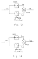
- Figure 14 shows the configuration of the PNC 1309 shown in Figure 13, and shows the same configuration as that of the first embodiment shown in Figure 12.
- an unmodulated subcarrier component having the frequency f if - f ref is extracted from the received intermediate frequency signal. Then, the phase comparison is performed between the subcarrier component and the received intermediate frequency signal, thereby canceling phase noise.
- the received intermediate frequency signal is branched to two routes.
- the received intermediate frequency signal is delayed by a delay circuit 1401.
- an unmodulated subcarrier component having the frequency f if - f ref is extracted by a band-pass filter 1402.
- An input signal in each route is mixed by a multiplier 1403, thereby obtaining the intermediate frequency signal with phase noise canceled.
- phase noise canceling method based on the configuration shown in Figure 14 is explained below.
- the following explanation describes how the light modulator 1303 shown in Figure 13 modulates a light in the PM method.
- a 12 , A 12 ', A 12 '', A 13 , and A 14 indicate predetermined constants.
- An intermediate frequency signal I 14 applied by the amplifier 1308 shown in Figure 13 can be represented by the following equation (19).
- D i (1 ⁇ i ⁇ N) indicates a data signal in each channel
- f if indicates a main carrier frequency in the IF stage
- f i (1 ⁇ i ⁇ N) indicates a carrier frequency in the electric stage corresponding to each channel (refer to Figure 10)
- f ref indicates an unmodulated carrier frequency in the electric stage
- (f if - f i ) indicates a subcarrier frequency modulated by the data signal D i in the IF stage
- (f if - f ref ) indicates an unmodulated subcarrier frequency in the IF stage
- m indicates a PM modulation index
- ⁇ (t) indicates a phase noise to be canceled
- Bessel function of the first kind indicates a data signal in each channel
- f if indicates a main carrier frequency in the IF stage
- f i (1 ⁇ i ⁇ N) indicates a carrier frequency in the electric
- the intermediate frequency signal I 14 is branched to two routes.
- an intermediate frequency signal I 15 delayed by the delay circuit 1401 in the first route can be represented by the following equation (20) according to equation (19).
- _t 1 indicates the delay time in the delay circuit 1401 as in the case shown in Figure 12.
- the BPF 1402 in the second route passes only the frequency component f if - f ref close to the frequency of the unmodulated subcarrier component.
- An intermediate frequency signal I 16 outputted therefrom can be represented by the following equation according to equation 19.
- I 16 A 13 J 1 (m)cos ⁇ 2 ⁇ (f if - f ref ) t + ⁇ (t) ⁇ where a time delay arises when an intermediate frequency signal is transmitted through the BPF 1402.
- an output I 16 of the BPF 1402 can be represented by the following equation (21) according to the equation above, where ⁇ t 2 indicates the time delay.
- I 16 A 13 J 1 (m)cos ⁇ 2 ⁇ (f if - f ref ) (t - ⁇ t 2 ) + ⁇ (t - ⁇ t 2 ) ⁇
- an intermediate frequency signal I 16 which is an unmodulated subcarrier component, can be regenerated from the second route.
- a component I 17 in the detection band can be represented by the following equation (22) according to the above equations (20) and (21).
- I 17 A 14 ⁇ cos ⁇ 2 ⁇ (f if - f ref ) ( ⁇ t 1 - ⁇ t 2 ) - 2 ⁇ (f ref - f i ) (t - ⁇ t 1 ) + D i (t - ⁇ t 1 ) - ⁇ ( ⁇ t 1 - ⁇ t 2 ) ⁇ where ⁇ ( ⁇ t 1 - ⁇ t 2 ) and ⁇ 2 distributed therefrom can be obtained in the same manner as in equations (6) and (7) shown in Figure 3.
- the phase noise component ⁇ ( ⁇ t 1 - ⁇ t 2 ) can be set to 0 by controlling the delay circuit 1401 such that the delay time ⁇ t 1 in the delay circuit 1402 equals the time delay ⁇ t 2 in the BPF 1402. Accordingly, the output I 17 from the multiplier 1403 shown in equation (22) above can be represented by the following equation (23).
- I 17 A 14 ⁇ cos ⁇ -2 ⁇ (f ref - f i ) (t - ⁇ t 1 ) + D i (t - ⁇ t 1 ) ⁇ where the intermediate frequency signal I 17 is applied to each of the DEMODs 1310-1 - 1310-N shown in Figure 13, thereby demodulating the data signal D i with phase noise canceled.
- the intermediate frequency signal I 17 which is a demodulated signal, output from the multiplier 1403 is not affected at all as long as the delay time ⁇ t 1 in the delay circuit 1401 equals the time delay _t 2 in the BPF 1402 although the frequency f if is changed, that is, the center light frequency f s of an modulated light generated by the light modulator 1303 or the light frequency f L in the local oscillator light obtained by the Lo-LD 1306 is changed.
- the channel interval can be reduced in the sending equipment for double the data transmission rate. Therefore, all or a plurality of channels can be collectively received in the receiving equipment without a broadband receiver, thereby largely increasing the number of receivable channels at a low cost.
- the modulated light transmitted through the optical fiber 1304 is obtained by directly modulating only one carrier light according to a microwave multiplexing signal for a plurality of channels.
- it can be obtained by directly modulating a number of carrier lights having different frequencies (wavelengths) according to a microwave multiplexing signal for a plurality of channels, and by light-frequency-multiplexing (wavelength-multiplexing) these carrier lights.
- Figure 15 shows the configuration of the third embodiment of the present invention. It shows the system configuration in which the present invention is applied to a light distributing network through a coherent SCM optical communication system.
- a modulator (MOD) 1501-1 - 1501-N In a transmitter A such as a central office (CO) and a head end (HE) shown in Figure 15, a modulator (MOD) 1501-1 - 1501-N, a multiplexer 1502, and a light modulator 1503 respectively correspond to the sending sides of the units 1301-1 - 1301 - N, 1302, and 1303 in the coherent SCM optical communication system represented as the second embodiment shown in Figure 13.
- CO central office
- HE head end
- a light receiver 1507, an amplifier 1508, a PNC 1509, and demodulating circuits (DEMOD) 1510-1 - 1510-N in the receiver (subscriber) respectively correspond to the receiving sides of the units 1307, 1308, 1309, and 1310-1 - 1310-N.
- a plurality of receivers C are connected to optical fibers 1504 through the distributors (repeaters) B such as the local office (LO), the hub, and the remote terminal (RT).
- the distributors (repeaters) B such as the local office (LO), the hub, and the remote terminal (RT).
- the mixing circuit 1305 and the Lo-LD 1306 provided on the receiving side as shown in Figure 13 respectively correspond to the units 1505 and 1506 shown in Figure 15. Thus, they are provided in a pair in the distributor B for a plurality of receivers C.
- a modulated signal from the light modulator 1503 in the transmitter A is led to the distributor B through the optical fibers 1504.
- a modulated light is mixed with a local oscillator light having the central light frequency of f L from the Lo-LD 1506. Then, the mixed light is branched and transmitted to each receiver C through the optical fibers.
- an intermediate frequency signal which is optical-heterodyne-detected from the light detector 1507 can be obtained.
- the intermediate frequency signal is amplified by the amplifier 1508 and applied to the PNC 1509 which has the same configuration as that shown in Figure 14 for the second embodiment and cancels phase noises contained in an intermediate frequency signal.
- the intermediate frequency signal is branched for the number of channels.
- Each of the demodulators 1510-1 - 1510-N extracts from each of the intermediate frequency signals as branched above each subcarrier component close to each of the center frequencies of f ref - f 1 , f ref - f 2 , ..., f ref - f N . Then, data signals D 1 - D N are demodulated.
- a local oscillator In a common optical heterodyne detection, a local oscillator (Lo-LD) is normally provided close to the light so as to maximize the power to be applied to the light detector.
- a distributor B In an optical distribution system, a distributor B is located about a few kilometers apart from a receiver C, resulting in a-few-decibel loss (for a single mode fiber) caused by the optical transmission of a modulated signal.
- the Lo-LD 1506 is provided in the distributor B so that the mixed light obtained by mixing the modulated light with the locally generated light in the distributor B can be directly transmitted to the receiver C through fiber branches. If the deterioration in the receiving sensitivity must be minimized, the branch loss should be compensated by a light amplifier provided before or after a light branch.
- a signal light and a local oscillator light can be collectively mixed for a plurality of receivers C by a single Lo-LD 1506 provided in the distributor B. Therefore, the cost per receiver can be much reduced, and a light distributing network can be realized through a low-cost coherent SCM optical communication system.
- the channel interval can be reduced in the sending equipment for double the data transmission rate. Therefore, all or a plurality of channels can be collectively received in the receiving equipment without a broadband receiver, thereby largely increasing the number of receivable channels at a low cost in a light distributing network.
- the modulated light transmitted through the optical fiber 1504 is obtained by directly modulating only one carrier light according to a microwave multiplexing signal for a plurality of channels.
- it can be obtained by directly modulating a number of carrier lights having different frequencies (wavelengths) according to a microwave multiplexing signal for a plurality of channels, and by light-frequency-multiplexing (wavelength-multiplexing) these carrier lights.
- the number of receivable channels can be further increased.
- Figure 16 shows the configuration of the fourth embodiment of the present invention. As in the third embodiment shown in Figure 15, it shows the system configuration in which the present invention is applied to a light distributing network through a coherent SCM optical communication system. Specifically, the configuration includes a countermeasure to polarization.
- the polarization of the modulated light must coincide with that of the local oscillator light. If they are not coincident, the detection cannot be performed at all when they are linear polarization orthogonal to each other.
- measure (1) is not applicable because polarization maintaining fibers are expensive, and the already mounted optical fibers become inapplicable.
- Measure (2) is effective in a common coherent optical transmission system, but it requires each subscriber have two receivers in a coherent SCM optical communication system, and thus is expensive. Besides, when Lo-LD and a receiver are mounted apart (refer to the third embodiment shown in Figure 15), it is difficult to feed back to a Lo-LD an intermediate frequency signal received by a receiver.
- Measure (3) controls the polarization state of the local oscillator light obtained by the Lo-LD in a distributor such that a mixed light is monitored in the distributor and a resultant monitor signal indicates the maximum power.
- a high receiving sensitivity can be obtained, however, it is technically difficult to perform polarization control of random polarization fluctuation of the modulated light transmitted through optical fibers, and is expensive.
- the polarization state of the modulated light obtained by the light modulator is scrambled by the polarization scrambler provided after the light modulator in the transmitter, and then, the modulated light is transmitted to the optical fibers.
- the polarization scrambler provided after the light modulator in the transmitter, and then, the modulated light is transmitted to the optical fibers.
- Figure 16 shows the fourth embodiment of a light distributing network through a coherent SCM optical communication system provided with a countermeasure to polarization to prevent the above described problems when the present invention is applied.
- the fourth embodiment shown in Figure 16 is different from the third embodiment shown in Figure 15 in the following point.
- the mixing circuit 1505 and the Lo-LD 1506 are provided in the distributor B, and a local oscillator light is collectively mixed with a signal light in the distributor B for a plurality of receivers C.
- a mixing circuit 1601 and an Lo-LD 1602 are provided in a transmitter A, and the polarization controller 1603 controls the polarization state of the local oscillator light such that the polarization state of the modulated light from the light modulator 1503 coincides with that of the local oscillator light from the Lo-LD 1602.
- the fourth embodiment is, as in the third embodiment, featured by that a single Lo-LD 1602 enables the local oscillator light and the signal light to be collectively mixed for a plurality of receivers C, that it is a coherent SCM optical communication system capable of largely increasing the number of receivable channels in a light distributing network at a low cost, and that precise polarization control can be performed in the transmitter A.
- a modulated light transmitted through the optical fiber 1504 is obtained by directly modulating a carrier light according to a microwave multiplexing signal for a plurality of channels. It can be also obtained by directly modulating a number of carrier lights having different frequencies (wavelengths) according to a microwave multiplexing signal for a plurality of channels, by mixing each of the carrier lights after being polarization-controlled as described above, and by light-frequency-multiplexing (wavelength multiplexing) them. With this configuration, the number of receivable channels can be increased as in the third embodiment.
- the configuration in which a mixing circuit, an Lo-LD, and a polarization controller are provided in a transmitter as described above can be applicable, not only to a light distributing network shown in Figure 16, but to a one-to-one optical communication system in which no distributors are provided between a transmitter and a receiver as in the second embodiment shown in Figure 13.
- Figure 17 shows the configuration of the fifth embodiment of the present invention.
- the fifth embodiment of the present invention can be applicable to a light distributing network through a coherent SCM optical communication system provided with a countermeasure to polarization.
- the fifth embodiment shown in Figure 17 is different from the fourth embodiment shown in Figure 16 in that a light amplifier (O.A.) 1701 is provided as a post-amplifier in the transmitter A.
- a light amplifier (O.A.) 1701 is provided as a post-amplifier in the transmitter A.
- the signal power from the transmitter A can be amplified, the system margin is increased, and the transmission distance is extended and the number of branches is increased in a light distributing network.
- Figure 18 shows the configuration of the sixth embodiment of the present invention.
- the present invention is applied to a light distributing network through a coherent SCM optical communication system provided with a countermeasure to polarization in the sixth embodiment.
- the light amplifier 1701 is provided as a post-amplifier in the transmitter A, while a light amplifier 1801 is provided before the light branch in the distributor B in the sixth embodiment shown in Figure 18.
- the branch loss caused by the distributor B can be compensated by the light amplifier 1801, thereby increasing the number of branches.
- a signal can be amplified by a light amplifier for each line after a light branch.
- the light amplifiers can be provided before and after the light branch. Additionally, these configurations can be mixed with the configuration of the fifth embodiment shown in Figure 17 in which the light amplifier is provided in the transmitter A.
- the frequency component of an unmodulated signal composed in the sending equipment is regenerated in a phase noise cancelling process without regenerating components in the broad frequency band from the frequency component of a frequency-multiplexed signal to the main carrier component when the optical heterodyne or homodyne detection, for example, is performed.
- a broadband circuit is not required as a light receiving unit, thereby considerably reducing the total cost for the whole system.
- the demodulating function is not affected at all in the demodulating unit as long as the delay time in the delay unit equals the signal delay time in the unmodulated component extracting unit although the frequency of the main carrier component is changed, that is, the center light frequency of a modulated light or the frequency of a local oscillator light in the light receiving unit is changed. Accordingly, the requirements for the oscillation frequency from the local oscillating unit in the light modulating unit or the light receiving unit can be considerably reduced, thereby minimizing the cost for the whole system.
- the channel interval (frequency interval) of each transmission signal multiplexed at a microwave level in the sending equipment can be reduced to approximately the double each data transmission rate for a digital signal, for example.
- the receiving equipment collectively receives all or a plurality of channels without need for a broadband receiver, thereby greatly increasing the number of receiving channels at a low cost.
- a local oscillator unit as a part of a light receiving unit and a mixing unit are provided in a repeater when the repeater (distributor) is only a few kilometers apart from each of the receivers, thereby transmitting to each receiver according to the branches of fibers a mixed light obtained by mixing a modulated light and a local oscillator light in the distributor directly.
- a specific mixing unit is not required at each receiver, thereby considerably reducing the cost for each receiver and practically realizing a light distributing network through a low-cost coherent SCM optical communication system.
- the system margin can be improved by providing a light amplifier as a light post-amplifier in the output unit of the transmitter or by providing a light amplifier before or after a light branch in the repeater in the light distributing network, thereby extending the transmission distance and increasing the number of distributions.
Landscapes
- Engineering & Computer Science (AREA)
- Computer Networks & Wireless Communication (AREA)
- Signal Processing (AREA)
- Optical Communication System (AREA)
Applications Claiming Priority (3)
| Application Number | Priority Date | Filing Date | Title |
|---|---|---|---|
| JP23430291A JP3183685B2 (ja) | 1991-09-13 | 1991-09-13 | 光通信システム |
| JP23430291 | 1991-09-13 | ||
| JP234302/91 | 1991-09-13 |
Publications (3)
| Publication Number | Publication Date |
|---|---|
| EP0532021A2 EP0532021A2 (en) | 1993-03-17 |
| EP0532021A3 EP0532021A3 (en) | 1993-06-02 |
| EP0532021B1 true EP0532021B1 (en) | 2001-01-10 |
Family
ID=16968871
Family Applications (1)
| Application Number | Title | Priority Date | Filing Date |
|---|---|---|---|
| EP92115569A Expired - Lifetime EP0532021B1 (en) | 1991-09-13 | 1992-09-11 | Coherent subcarrier multiplexed optical communication system |
Country Status (5)
| Country | Link |
|---|---|
| US (1) | US5432632A (ja) |
| EP (1) | EP0532021B1 (ja) |
| JP (1) | JP3183685B2 (ja) |
| CA (1) | CA2078076C (ja) |
| DE (1) | DE69231632T2 (ja) |
Families Citing this family (37)
| Publication number | Priority date | Publication date | Assignee | Title |
|---|---|---|---|---|
| US5351147A (en) * | 1992-10-27 | 1994-09-27 | Bell Communications Research, Inc. | Pulse frequency division multiplexing |
| KR970003527B1 (ko) * | 1994-05-14 | 1997-03-18 | 재단법인 한국전자통신연구소 | 파장분할 다중화 방식을 이용한 양방향 다채널 광 링 통신망 |
| DE4444218A1 (de) * | 1994-12-13 | 1996-06-27 | Sel Alcatel Ag | Optische Sendeeinrichtung für ein optisches Nachrichtenübertragungssystem in Verbindung mit einem Funksystem |
| US5596436A (en) * | 1995-07-14 | 1997-01-21 | The Regents Of The University Of California | Subcarrier multiplexing with dispersion reduction and direct detection |
| US6271942B1 (en) * | 1996-11-26 | 2001-08-07 | Matsushita Electric Industrial Co., Ltd. | Optical transmission device and system |
| US6459519B1 (en) * | 1997-04-09 | 2002-10-01 | Matsushita Electric Industrial Co., Ltd. | Optical transmitter-receiver |
| JP4184474B2 (ja) * | 1997-08-22 | 2008-11-19 | 松下電器産業株式会社 | 光伝送システムならびにそれに用いられる光送信装置および光受信装置 |
| DE19737482A1 (de) | 1997-08-28 | 1999-03-04 | Alsthom Cge Alcatel | Verfahren zur optischen Übertragung über ein Lichtwellenleiternetz, sowie optisches Übertragungsnetz |
| US7130540B2 (en) * | 1998-07-21 | 2006-10-31 | Corvis Corporation | Optical transmission systems, devices, and methods |
| US6449073B1 (en) | 1998-07-21 | 2002-09-10 | Corvis Corporation | Optical communication system |
| US6529305B1 (en) | 1998-11-04 | 2003-03-04 | Corvis Corporation | Optical transmission apparatuses, methods, and systems |
| US6118566A (en) * | 1998-11-04 | 2000-09-12 | Corvis Corporation | Optical upconverter apparatuses, methods, and systems |
| US6292598B1 (en) | 1998-11-04 | 2001-09-18 | Corvis Corporation | Optical transmission apparatuses, methods, and systems |
| JP2000323786A (ja) * | 1999-05-14 | 2000-11-24 | Fujitsu Ltd | 信号光の波形整形のための方法、装置及びシステム |
| US6771905B1 (en) | 1999-06-07 | 2004-08-03 | Corvis Corporation | Optical transmission systems including optical switching devices, control apparatuses, and methods |
| US20010021047A1 (en) * | 1999-12-24 | 2001-09-13 | Hiroyuki Sasai | Optical transmission system and optical receiver |
| JP3338013B2 (ja) * | 2000-01-12 | 2002-10-28 | 松下電器産業株式会社 | 光伝送システム及びこのシステムに用いる光送信装置 |
| AU2001273512A1 (en) * | 2000-08-03 | 2002-02-18 | Lockheed Martin Corporation | Phase shift keyed signaling with forward error correction and raman amplification in optical wdm links |
| GB0020624D0 (en) | 2000-08-21 | 2000-10-11 | Element 14 Inc | Multi band DMT receiver |
| US7068948B2 (en) * | 2001-06-13 | 2006-06-27 | Gazillion Bits, Inc. | Generation of optical signals with return-to-zero format |
| US7142788B2 (en) * | 2002-04-16 | 2006-11-28 | Corvis Corporation | Optical communications systems, devices, and methods |
| US6922529B2 (en) * | 2002-08-09 | 2005-07-26 | Corvis Corporation | Optical communications systems, devices, and methods |
| US7088885B1 (en) * | 2002-11-13 | 2006-08-08 | Finisar Corporation | System for modulating optical signals |
| US7761011B2 (en) * | 2005-02-23 | 2010-07-20 | Kg Technology Associates, Inc. | Optical fiber communication link |
| US7826752B1 (en) * | 2005-06-02 | 2010-11-02 | Level 3 Communications, Llc | Optical transmission apparatuses, methods, and systems |
| US20080019704A1 (en) * | 2006-05-31 | 2008-01-24 | Campillo Anthony L | Interferometer-based chromatic dispersion monitor |
| US20080310846A1 (en) * | 2007-06-13 | 2008-12-18 | West Jr Lamar E | Frequency modulated burst mode transmitter |
| JP2009177641A (ja) | 2008-01-25 | 2009-08-06 | Fujitsu Ltd | 光信号処理装置、光受信装置および光中継装置 |
| US8676056B2 (en) * | 2008-06-20 | 2014-03-18 | Xieon Networks S.A.R.L. | Subcarrier multiplex system |
| EP2495612B1 (en) * | 2009-10-30 | 2019-11-27 | Fujitsu Limited | Optical signal processing device, receiver, and optical network system |
| CN102792613B (zh) * | 2010-03-19 | 2015-11-25 | 瑞典爱立信有限公司 | 光通信系统 |
| JP5549333B2 (ja) * | 2010-04-07 | 2014-07-16 | 富士通株式会社 | 偏波変動補償装置および光通信システム |
| JP5598168B2 (ja) * | 2010-08-30 | 2014-10-01 | 富士通株式会社 | 光ネットワークシステムおよび光多重装置 |
| JP5601144B2 (ja) * | 2010-10-20 | 2014-10-08 | 三菱電機株式会社 | 高周波発振器および高周波発振方法 |
| JP2013078093A (ja) * | 2011-09-30 | 2013-04-25 | Fujitsu Ltd | 光受信装置および光ネットワークシステム |
| CN111049585B (zh) | 2018-10-13 | 2022-06-14 | 华为技术有限公司 | 一种光收发器和光相干接收系统 |
| US10735128B1 (en) * | 2019-03-05 | 2020-08-04 | Rockwell Collins, Inc. | Optical phase sensitivity enhancement for reduced power |
Family Cites Families (8)
| Publication number | Priority date | Publication date | Assignee | Title |
|---|---|---|---|---|
| US3532889A (en) * | 1967-08-28 | 1970-10-06 | Bell Telephone Labor Inc | Light communication system with improved signal-to-noise ratio |
| US4287606A (en) * | 1980-09-17 | 1981-09-01 | Nasa | Fiber optic transmission line stabilization apparatus and method |
| NL8800067A (nl) * | 1988-01-12 | 1989-08-01 | Nederland Ptt | Werkwijze en inrichting voor het, in een coherent optisch communicatie systeem met heterodyne detectie, aan ontvangstzijde compenseren van faseruis van zend en lokale laser. |
| JPH01212932A (ja) * | 1988-02-19 | 1989-08-25 | Fujitsu Ltd | Dpsk変調ヘテロダイン検波方式 |
| US4953156A (en) * | 1988-09-08 | 1990-08-28 | Gte Laboratories, Incorporated | Wideband subcarrier multiplexed optical communication system operating over more than one octave |
| JPH0734080B2 (ja) * | 1988-10-20 | 1995-04-12 | 富士通株式会社 | コヒーレント光通信用ヘテロダイン検波受信装置 |
| US5134509A (en) * | 1988-12-22 | 1992-07-28 | Gte Laboratories Incorporated | Coherent subcarrier multiplexed optical communication system |
| US4989200A (en) * | 1988-12-22 | 1991-01-29 | Gte Laboratories Incorporated | Coherent subcarrier multiplexed optical communication system |
-
1991
- 1991-09-13 JP JP23430291A patent/JP3183685B2/ja not_active Expired - Fee Related
-
1992
- 1992-09-11 CA CA002078076A patent/CA2078076C/en not_active Expired - Fee Related
- 1992-09-11 DE DE69231632T patent/DE69231632T2/de not_active Expired - Fee Related
- 1992-09-11 EP EP92115569A patent/EP0532021B1/en not_active Expired - Lifetime
- 1992-09-14 US US07/944,203 patent/US5432632A/en not_active Expired - Lifetime
Also Published As
| Publication number | Publication date |
|---|---|
| JPH0575540A (ja) | 1993-03-26 |
| EP0532021A2 (en) | 1993-03-17 |
| CA2078076A1 (en) | 1993-03-14 |
| JP3183685B2 (ja) | 2001-07-09 |
| CA2078076C (en) | 1998-07-28 |
| DE69231632D1 (de) | 2001-02-15 |
| US5432632A (en) | 1995-07-11 |
| EP0532021A3 (en) | 1993-06-02 |
| DE69231632T2 (de) | 2001-06-13 |
Similar Documents
| Publication | Publication Date | Title |
|---|---|---|
| EP0532021B1 (en) | Coherent subcarrier multiplexed optical communication system | |
| US5896211A (en) | Optical communication system | |
| US4959826A (en) | Spread spectrum optical communication system with heterodyne detection | |
| US5305134A (en) | Optical frequency division multiplexing transmitter and optical frequency division multiplexing transmission apparatus | |
| US5546190A (en) | Carrier and clock recovery for lightwave systems | |
| JP2679953B2 (ja) | 高密度光波長分割多重化 | |
| US6118565A (en) | Coherent optical communication system | |
| Kuri et al. | Optical heterodyne detection technique for densely multiplexed millimeter-wave-band radio-on-fiber systems | |
| CA2242072C (en) | Remote monitoring of an optical transmission system using line monitoring signals | |
| CA2058580A1 (en) | Optical modulator for cancellation of second-order intermodulation products in lightwave systems | |
| US6850710B1 (en) | Method and apparatus of utilizing RF/microwave and optical mixing techniques to select a given band of an optical transmission | |
| EP0201825A2 (en) | Optical fiber communication with Frequency-Division-Multiplexing | |
| WO1998009397A1 (en) | Simultaneous wavelength-division multiplexing and broadcast transmission system | |
| CA2375773A1 (en) | Method and apparatus of utilizing rf/microwave mixing techniques to select a given band of an optical transmission | |
| US5390043A (en) | Compressed channel spacing for optical heterodyne communication systems | |
| JPH0779310B2 (ja) | 光通信システム | |
| US5796503A (en) | Optical communication system wherein optical beat interference at the center is reduced | |
| JP3368935B2 (ja) | 光伝送装置 | |
| JP2775692B2 (ja) | 光通信方式 | |
| Shibagaki et al. | Video transmission characteristics in WDM star networks | |
| JPH02210925A (ja) | 基本帯域ディジタル信号および多重マイクロ波副搬送波の同時伝送用光通信システム | |
| JPH09129950A (ja) | 光受信装置 | |
| JP3025544B2 (ja) | 光通信システム | |
| JP2000059340A (ja) | スペクトルコ―ド化デ―タ伝送システムで使われる受信機とその方法 | |
| JP2004088159A (ja) | 変調された光信号の多重伝送方法およびその装置 |
Legal Events
| Date | Code | Title | Description |
|---|---|---|---|
| PUAI | Public reference made under article 153(3) epc to a published international application that has entered the european phase |
Free format text: ORIGINAL CODE: 0009012 |
|
| AK | Designated contracting states |
Kind code of ref document: A2 Designated state(s): DE FR GB |
|
| PUAL | Search report despatched |
Free format text: ORIGINAL CODE: 0009013 |
|
| AK | Designated contracting states |
Kind code of ref document: A3 Designated state(s): DE FR GB |
|
| 17P | Request for examination filed |
Effective date: 19931130 |
|
| 17Q | First examination report despatched |
Effective date: 19970506 |
|
| GRAG | Despatch of communication of intention to grant |
Free format text: ORIGINAL CODE: EPIDOS AGRA |
|
| GRAG | Despatch of communication of intention to grant |
Free format text: ORIGINAL CODE: EPIDOS AGRA |
|
| GRAH | Despatch of communication of intention to grant a patent |
Free format text: ORIGINAL CODE: EPIDOS IGRA |
|
| GRAH | Despatch of communication of intention to grant a patent |
Free format text: ORIGINAL CODE: EPIDOS IGRA |
|
| GRAA | (expected) grant |
Free format text: ORIGINAL CODE: 0009210 |
|
| AK | Designated contracting states |
Kind code of ref document: B1 Designated state(s): DE FR GB |
|
| REF | Corresponds to: |
Ref document number: 69231632 Country of ref document: DE Date of ref document: 20010215 |
|
| ET | Fr: translation filed | ||
| PLBE | No opposition filed within time limit |
Free format text: ORIGINAL CODE: 0009261 |
|
| STAA | Information on the status of an ep patent application or granted ep patent |
Free format text: STATUS: NO OPPOSITION FILED WITHIN TIME LIMIT |
|
| REG | Reference to a national code |
Ref country code: GB Ref legal event code: IF02 |
|
| 26N | No opposition filed | ||
| PGFP | Annual fee paid to national office [announced via postgrant information from national office to epo] |
Ref country code: FR Payment date: 20080915 Year of fee payment: 17 |
|
| PGFP | Annual fee paid to national office [announced via postgrant information from national office to epo] |
Ref country code: GB Payment date: 20080917 Year of fee payment: 17 |
|
| PGFP | Annual fee paid to national office [announced via postgrant information from national office to epo] |
Ref country code: DE Payment date: 20080926 Year of fee payment: 17 |
|
| GBPC | Gb: european patent ceased through non-payment of renewal fee |
Effective date: 20090911 |
|
| REG | Reference to a national code |
Ref country code: FR Ref legal event code: ST Effective date: 20100531 |
|
| PG25 | Lapsed in a contracting state [announced via postgrant information from national office to epo] |
Ref country code: DE Free format text: LAPSE BECAUSE OF NON-PAYMENT OF DUE FEES Effective date: 20100401 Ref country code: FR Free format text: LAPSE BECAUSE OF NON-PAYMENT OF DUE FEES Effective date: 20090930 |
|
| PG25 | Lapsed in a contracting state [announced via postgrant information from national office to epo] |
Ref country code: GB Free format text: LAPSE BECAUSE OF NON-PAYMENT OF DUE FEES Effective date: 20090911 |