EP0529612B1 - A camera apparatus having self timer function - Google Patents
A camera apparatus having self timer function Download PDFInfo
- Publication number
- EP0529612B1 EP0529612B1 EP92114565A EP92114565A EP0529612B1 EP 0529612 B1 EP0529612 B1 EP 0529612B1 EP 92114565 A EP92114565 A EP 92114565A EP 92114565 A EP92114565 A EP 92114565A EP 0529612 B1 EP0529612 B1 EP 0529612B1
- Authority
- EP
- European Patent Office
- Prior art keywords
- signal
- output
- shutter
- timer
- circuit
- Prior art date
- Legal status (The legal status is an assumption and is not a legal conclusion. Google has not performed a legal analysis and makes no representation as to the accuracy of the status listed.)
- Expired - Lifetime
Links
Images






Classifications
-
- G—PHYSICS
- G04—HOROLOGY
- G04F—TIME-INTERVAL MEASURING
- G04F13/00—Apparatus for measuring unknown time intervals by means not provided for in groups G04F5/00 - G04F10/00
- G04F13/02—Apparatus for measuring unknown time intervals by means not provided for in groups G04F5/00 - G04F10/00 using optical means
-
- H—ELECTRICITY
- H04—ELECTRIC COMMUNICATION TECHNIQUE
- H04N—PICTORIAL COMMUNICATION, e.g. TELEVISION
- H04N23/00—Cameras or camera modules comprising electronic image sensors; Control thereof
- H04N23/60—Control of cameras or camera modules
- H04N23/63—Control of cameras or camera modules by using electronic viewfinders
-
- H—ELECTRICITY
- H04—ELECTRIC COMMUNICATION TECHNIQUE
- H04N—PICTORIAL COMMUNICATION, e.g. TELEVISION
- H04N23/00—Cameras or camera modules comprising electronic image sensors; Control thereof
- H04N23/70—Circuitry for compensating brightness variation in the scene
-
- H—ELECTRICITY
- H04—ELECTRIC COMMUNICATION TECHNIQUE
- H04N—PICTORIAL COMMUNICATION, e.g. TELEVISION
- H04N23/00—Cameras or camera modules comprising electronic image sensors; Control thereof
- H04N23/70—Circuitry for compensating brightness variation in the scene
- H04N23/73—Circuitry for compensating brightness variation in the scene by influencing the exposure time
-
- H—ELECTRICITY
- H04—ELECTRIC COMMUNICATION TECHNIQUE
- H04N—PICTORIAL COMMUNICATION, e.g. TELEVISION
- H04N23/00—Cameras or camera modules comprising electronic image sensors; Control thereof
- H04N23/80—Camera processing pipelines; Components thereof
- H04N23/84—Camera processing pipelines; Components thereof for processing colour signals
-
- H—ELECTRICITY
- H04—ELECTRIC COMMUNICATION TECHNIQUE
- H04N—PICTORIAL COMMUNICATION, e.g. TELEVISION
- H04N25/00—Circuitry of solid-state image sensors [SSIS]; Control thereof
- H04N25/10—Circuitry of solid-state image sensors [SSIS]; Control thereof for transforming different wavelengths into image signals
- H04N25/11—Arrangement of colour filter arrays [CFA]; Filter mosaics
- H04N25/13—Arrangement of colour filter arrays [CFA]; Filter mosaics characterised by the spectral characteristics of the filter elements
- H04N25/135—Arrangement of colour filter arrays [CFA]; Filter mosaics characterised by the spectral characteristics of the filter elements based on four or more different wavelength filter elements
- H04N25/136—Arrangement of colour filter arrays [CFA]; Filter mosaics characterised by the spectral characteristics of the filter elements based on four or more different wavelength filter elements using complementary colours
-
- H—ELECTRICITY
- H04—ELECTRIC COMMUNICATION TECHNIQUE
- H04N—PICTORIAL COMMUNICATION, e.g. TELEVISION
- H04N5/00—Details of television systems
- H04N5/222—Studio circuitry; Studio devices; Studio equipment
- H04N5/262—Studio circuits, e.g. for mixing, switching-over, change of character of image, other special effects ; Cameras specially adapted for the electronic generation of special effects
- H04N5/2628—Alteration of picture size, shape, position or orientation, e.g. zooming, rotation, rolling, perspective, translation
Definitions
- the present invention relates to a camera apparatus in which a video camera and a photographic camera are integrally combined and which has a self-timer function.
- FIG. 14 shows an example of an arrangement of a shutter system for a conventional still video camera.
- a shutter switch 201 is connected to a shutter trigger generating circuit 202, and when the shutter switch 201 is turned on, the trigger generating circuit 202 outputs a shutter trigger signal.
- the shutter trigger signal is supplied to a synchronous circuit 204 via a fixed terminal N of a changeover switch 203.
- the synchronous circuit 204 is also supplied with a vertical synchronizing signal VD, and after being supplied with the shutter trigger signal, it outputs a record pulse PREC in synchronism with the synchronizing signal VD, the record pulse PREC being supplied to a fixed terminal N of a changeover switch 205.
- a self-timer standby switch 206 is connected to a mode detection circuit 207.
- a normal shutter mode normal mode
- a self-timer mode self mode
- the changeover switches 203 and 205 are connected to the respective terminals N, and when the self mode is detected, the switches 203 and 205 are connected to the respective terminals S and a timer 208 is set in an operative state.
- the shutter trigger signal output from the trigger generating circuit 202 is supplied to the timer 208 as a timer start signal through the fixed terminal S of the changeover switch 203.
- the timer 208 generates a pulse signal upon lapse of a predetermined period TO after the shutter trigger signal is supplied thereto, the pulse signal being supplied to a shutter trigger generating circuit 209.
- the trigger generating circuit 209 then outputs a shutter trigger signal to a synchronous circuit 210.
- the synchronous circuit 210 is supplied with the vertical synchronizing signal VD, and after being supplied with the shutter trigger signal, it outputs a record pulse PREC in synchronism with the synchronising signal VD, the record pulse PREC being supplied to the fixed terminal S of the changeover switch 205.
- the shutter switch 201 while in the normal mode in which the standby switch 206 is off, if the shutter switch 201 is turned on, the shutter trigger signal generated by the trigger generating circuit 202 is supplied to the synchronous circuit 204 through the fixed terminal N of the changeover switch 203. Therefore, the record pulse PREC generated by the synchronous circuit 204 is output through the fixed terminal N of the changeover switch 205.
- the shutter trigger signal generated by the trigger generating circuit 202 is supplied to the timer 208 through the fixed terminal S of the changeover switch 203.
- the trigger generating circuit 209 outputs a shutter trigger signal to the synchronous circuit 210.
- the record pulse PREC generated by the synchronous circuit 210 is output through the fixed terminal S of the changeover switch 205.
- the above-described shutter system is applied to a still video camera, but it is equally applicable to a photographic (film) camera.
- the record pulse PREC can be used as a drive pulse (shutter pulse) for the shutter mechanism.
- the circuitry for the normal mode is separate from that for the self mode.
- the arrangement includes two shutter trigger generating circuits 202 and 209, two synchronous circuits 204 and 210, and two changeover switches 203 and 205, thus making the circuit configuration of the shutter system complicated.
- a still image in addition to a dynamic image, can be acquired.
- the resolution of video cameras is poorer than that of photographic cameras, and there is a demand for a combined use of a video camera and a photographic camera.
- a photographic camera may be fixed to a video camera so that an image can be photographed by the photographic camera while a dynamic image is acquired by the video camera.
- Such a camera apparatus including a video camera and a photographic camera may be designed to operate in a still mode for obtaining a still image and in a video mode for obtaining a dynamic image.
- a still image can be acquired by both the video camera and the photographic camera, and therefore, in the still mode, the record pulse and the shutter pulse may be generated in response to an operation of the shutter switch.
- a dynamic image can be acquired by the video camera, and thus, in the video mode, the record pulse may be generated in response to an operation of the record switch. Further, there may be a situation where an image is photographed by the photographic camera while a dynamic image is acquired by the video camera, and therefore, the shutter pulse may be generated in response to an operation of the shutter switch.
- An object of the present invention is to provide a camera apparatus in which the circuit arrangement of a shutter system is simplified.
- a camera apparatus having a self-timer function comprises a frequency divider for carrying out a frequency division with respect to a vertical synchronizing signal, wherein an output signal of the frequency divider is used to drive a timer associated with the self-timer function and to obtain a shutter pulse.
- a shutter pulse synchronized with the vertical synchronizing signal can be obtained based on the output signal of the frequency divider. Further, in the self-timer mode, the timer is driven by the output signal of the frequency divider. Thus, the single frequency divider is used in both modes, and therefore, the circuit configuration of the shutter system is simplified.
- FIG. 1 is a perspective view showing an external appearance of the embodiment, wherein reference numeral 1 denotes a cabinet which has a built-in video camera section including an imaging device, a signal processing circuit, etc., and a built-in photographic camera section including a film loading mechanism, a film drive mechanism, etc., none of which are shown.
- reference numeral 1 denotes a cabinet which has a built-in video camera section including an imaging device, a signal processing circuit, etc., and a built-in photographic camera section including a film loading mechanism, a film drive mechanism, etc., none of which are shown.
- Reference numeral 2 denotes an imaging lens of the video camera section
- 3 denotes an imaging lens of the photographic camera section. Namely, an optical system for the video camera section is separate from that for the photographic camera section.
- a 6-power zoom lens having a focal length f of 7 to 42 mm is used for the imaging lens 2
- a fixed-focus lens having a focal length f of 55 mm is used for the imaging lens 3.
- an electronic viewfinder comprising a small-sized CRT is arranged in the cabinet 1, for displaying on the CRT an image picked up by the video camera section through the imaging lens 2.
- Reference numeral 4 represents an eyecup. There is provided no finder permitting a direct observation of an image to be photographed by the photographic camera section through the imaging lens 3.
- 5T and 5W denote zoom buttons for a Zooming operation in a TELE direction and a WIDE direction, respectively, 6 denotes a record button for recording a video signal output from the video camera section in a VTR, 7 denotes a shutter button, and 8 denotes a film rewind button.
- FIG. 2 shows the arrangement of the video camera section.
- An image light from an object enters through the imaging lens 2 and an iris 11 and falls upon a single-plate CCD solid-state imaging device 12 having a complementary checkered color filter.
- FIG. 3 shows in detail the arrangement of the zoom driver 41.
- reference numeral 411 denotes a lens forming the imaging lens 2 for adjusting the zooming power.
- the lens 411 can be moved back and forth when rotated, whereby the zooming power is adjusted. For example, if the lens 411 is rotated in a direction T, the zooming power changes in the TELE direction; if the lens is rotated in a direction W, the zooming power changes in the WIDE direction.
- the lens 411 is rotated by a DC motor 412, which has both ends connected to output terminals q1 and q2 of a zoom driver unit 413, respectively.
- Input terminals p1 and p2 of the zoom driver unit 413 are respectively connected to fixed terminals T and W of a zoom switch 42.
- a movable terminal of the zoom switch 42 is connected to a power supply terminal.
- the zoom switch 42 is connected to the terminal T or W, and a high-level "H" signal is supplied to the terminal p1 or p2 of the zoom driver unit 413, whereby the zooming power is adjusted in the TELE or WIDE direction.
- FIG. 4 is a schematic diagram showing color coding of the imaging device 12, and as illustrated, a field readout is carried out.
- a field charges are mixed in pairs, such as a pair of A1 and A2, and in B field, charges are mixed in pairs, such as a pair of B1 and B2.
- B field charges are mixed in pairs, such as a pair of B1 and B2.
- a field charges are output in order of A1, A2, ..., and for the B field in order of B1, B2, ..., from a horizontal shift register Hreg.
- the order of charges a, b, ... is (Cy + G), (Ye + Mg), ... in A1 line, (Cy + Mg), (Ye + G), ... in A2 line, (G + Cy), (Mg + Ye), ... in B1 line, and (Mg + Cy); (G + Ye), ... in B2 line.
- the output signal of the imaging device 12 is supplied to a CDS circuit (correlation double sampling circuit) 13 and is extracted thereby as an image signal.
- a CDS circuit correlation double sampling circuit
- Timing pulses needed by the imaging device 12 and the CDS circuit 13 are produced by a timing generator 14.
- the timing generator 14 is supplied with reference clock pulses CK0 at 8 fsc (fsc represents the color subcarrier frequency) from an oscillator 15, as well as horizontal and vertical synchronizing signals HD and VD from a synchronizing generator 16.
- the synchronizing generator 16 is supplied with clock pulses CK1 at 4 fsc from the timing generator 14.
- An image signal output from the CDS circuit 13 is supplied to a level detecting circuit 17, which outputs a signal to an iris driver 18.
- the iris driver 18 automatically controls the aperture of the iris 11.
- the luminance signal Y is obtained by adding adjacent signals together. Namely, referring to FIG. 5, summation signals are derived in sequence of a + b, b + c, c + d, d + e, ....
- the chroma signal is obtained by subjecting adjacent signals to a subtraction.
- a red differential signal R - Y and a blue differential signal -(B - Y) are alternately derived in a line sequential manner.
- the image signal output from the CDS circuit 13 is supplied to a low-pass filter 20 constituting a luminance processing unit through an AGC circuit 19.
- the low-pass filter 20 carries out an addition (averaging) of adjacent signals, and accordingly, a luminance signal Y is output therefrom.
- the image signal output from the AGC circuit 19 is supplied to sample holding circuits 21 and 22 forming a chroma processing unit.
- the sample holding circuits 21 and 22 are supplied with sampling pulses SHP1 and SHP2 (indicated at E and F in FIGS. 6 and 7), respectively, from the timing generator 14.
- SHP1 and SHP2 indicated at E and F in FIGS. 6 and 7
- FIG. 6 A shows the signal of the A1 line
- FIG. 7 shows the signal of the A2 line.
- the sample holding circuit 21 outputs a continuous signal S1 of (Cy + G) or (Cy + Mg) to a subtracter 23 (see B in FIGS. 6 and 7), and the sample holding circuit 22 outputs a continuous signal S2 of (Ye + Mg) or (Ye + G) to the subtracter 23 (see C in FIGS. 6 and 7).
- the subtracter 23 subtracts the signal S1 from the signal S2, whereby a red differential signal R - Y and a blue differential signal -(B - Y) are alternately output therefrom in a line sequential manner (as indicated at D in FIGS. 6 and 7).
- the color differential signals output from the subtracter 23 are supplied directly to a fixed terminal b of a changeover switch 24 and a fixed terminal a of a changeover switch 25, and also supplied to a fixed terminal a of the changeover switch 24 and a fixed terminal b of the changeover switch 25 via a delay circuit 26 having a delay time corresponding to one horizontal period.
- the switching operation of the changeover switches 24 and 25 is controlled by a controller 27. Specifically, the switches are connected to the respective terminals b during a horizontal period in which the red differential signal R - Y is output from the subtracter 23, and connected to the respective terminals a during a horizontal period in which the blue differential signal -(B - Y) is output.
- the controller 27 is supplied with the synchronizing signals HD and VD as reference synchronizing signals from the synchronizing generator 16, and the clock pulses CK1 from the timing generator 14.
- a red differential signal R - Y is output from the changeover switch 24 in each horizontal period and a blue differential signal -(B - Y) is output from the changeover switch 25 in each horizontal period.
- the luminance signal Y output from the low-pass filter 20 and the color differential signals (R - Y) and -(B - Y) output from the changeover switches 24 and 25 are supplied to an encoder 28.
- the encoder 28 is further supplied with a composite synchronizing signal SYNC, a blanking signal BLK, a burst flag signal BF, and a color subcarrier signal SC from the synchronizing generator 16.
- the luminance signal Y is combined with the synchronizing signal SYNC, and the color differential signals are subjected to quadrature two-phase modulation to form a carrier chrominance signal C and further combined with a color burst signal.
- the luminance signal Y and the carrier chrominance signal C are added together to form a color video signal SCV according to, e.g., the NTSC system.
- the color video signal SCV thus generated by the encoder 28 appears at an output terminal 29.
- the encoder 28 also generates a monochromatic video signal SV (i.e., the luminance signal Y combined with the synchronizing signal SYNC), which is supplied to an electronic viewfinder 30, and thus the acquired image is displayed at the small-sized CRT.
- a monochromatic video signal SV i.e., the luminance signal Y combined with the synchronizing signal SYNC
- the controller 27 is connected to a shutter switch 32 which turns on when the shutter button 7 is pressed, a record switch 34 which turns on when the record button 6 is pressed, a self-timer standby switch 33, and a mode changeover switch 35 for switching between a still mode for acquiring a still image and a video mode for acquiring a dynamic image.
- the still mode is set when the mode changeover switch 35 is connected to a terminal s, and the video mode is set when the switch 35 is connected to a terminal v.
- the controller 27 While in the still mode, if the shutter switch 32 is turned on when the standby switch 33 is off, the controller 27 immediately outputs a shutter pulse PSH and a record pulse PREC. On the other hand, while in the still mode, if the shutter switch 32 is turned on after the standby switch 33 is turned on, the controller 27 outputs a shutter pulse PSH and a record pulse PREC upon lapse of a predetermined time, whereby a self-timer function is achieved.
- the shutter pulse PSH is used to actuate the mechanical shutter of the photographic camera section (not shown), and the record pulse PREC is used to transfer a still image video signal to a still image recorder (not shown).
- a recorder using a DAT which the applicant proposed before (Unexamined Japanese Patent Publication No. 2-161661), may be used.
- the controller 27 While in the video mode, if the record switch 34 is turned on, the controller 27 immediately outputs a record pulse PREC. This record pulse PREC is used to control the recording operation of a recorder such as a VTR. Further, when the shutter switch 32 is turned on in the video mode, the controller 27 immediately outputs a shutter pulse PSH. This shutter pulse PSH is used to actuate the mechanical shutter of the photographic camera section, as in the still mode described above.
- FIGS. 8 and 9 show the arrangement of a shutter system (shutter pulse generating unit) of the controller 27.
- a series circuit composed of the self-timer standby switch 33 and a resistor 39 has one end connected to a power supply and the other end grounded, and a signal S33 obtained at the node P3 between the standby switch 33 and the resistor 39 is supplied to a self-timer controller 51.
- a self-timer mode is established when the standby switch 33 is turned on during a normal shutter mode, and the normal shutter mode is established when the standby switch 33 is turned on during the self-timer mode.
- the controller 51 outputs a signal S51a which is low-level “L” in the normal shutter mode and is high-level “H” in the self-timer mode, and also outputs signals S51b and S51e which are high-level "H” in the normal shutter mode and low-level “L” in the self-timer mode.
- the controller 51 When the shutter switch 32 is turned on in the self-timer mode, a count mode is set for a timer count period, and upon lapse of the timer count period, the normal shutter mode is automatically restored, as described later.
- the controller 51 further outputs a signal S51f which is high-level "H” during the timer count period and is low-level “L” during a period other than the timer count period, and a signal S51c which is set to high level "H” for a predetermined period subsequent to the timer count period.
- the controller 51 is supplied with a signal S68c, which is obtained by subjecting the vertical synchronizing signal VD (frequency: fv) to a frequency division of 1/128 at a frequency divider 68, mentioned later, as reference clock pulses for the timer.
- VD vertical synchronizing signal
- a series circuit composed of the shutter switch 32 and a resistor 52 is connected at one end to the power supply and grounded at the other end, and the node P1 between the shutter switch 32 and the resistor 52 is connected to one input terminal of an OR circuit 53.
- To the other input terminal of the OR circuit 53 is supplied the signal S51c output from the controller 51.
- the output signal of the OR circuit 53 is supplied to one input terminal of an AND circuit 54, and the signal S51b output from the controller 51 is supplied to the other input terminal of the AND circuit 54.
- the node P1 is connected to one input terminal of an AND circuit 55, the other input terminal of which is supplied with the signal S51a output from the controller 51.
- the output signal S55 of the AND circuit 55 is supplied to the controller 51.
- the output signal S54 of the AND circuit 54 is supplied to one input terminal of an AND circuit 56 and also to an integrating circuit composed of a resistor 57 and a capacitor 58.
- the output signal S54' of the integrating circuit is supplied to the other input terminal of the AND circuit 56 through an inverter 59, and the AND circuit 56 outputs a shutter signal S56.
- Another series circuit composed of the record switch 34 and a resistor 60 is connected at one end to the power supply and grounded at the other end, and the node P2 between the record switch 34 and the resistor 60 is connected to one input terminal of a NAND circuit 62 through an inverter 61.
- the output signal of the inverter 61 is supplied to an integrating circuit composed of a resistor 63 and a capacitor 64, and the output signal of the integrating circuit is supplied to the other input terminal of the NAND circuit 62 through an inverter 65.
- the output signal of the NAND circuit 62 is supplied to one input terminal of an AND circuit 66.
- the fixed terminal v of the mode changeover switch 35 is connected to the power supply, while the fixed terminal s of the same switch is grounded, and a signal S35 output from the movable terminal of the switch 35 is supplied to the other input terminal of the AND circuit 66.
- the AND circuit 66 outputs a record signal S66.
- the shutter signal S56 and the record signal S66, output respectively from the AND circuits 56 and 66, are supplied to an OR circuit 67, which then outputs a signal S67 to the aforesaid frequency divider 68.
- the frequency divider 68 is also supplied with the vertical synchronizing signal VD as a frequency-divided signal.
- the frequency divider 68 outputs a signal S68a obtained through a frequency division of 1/2, a signal S68b obtained through a frequency division of 1/64, and the aforesaid signal S68c obtained through a frequency division of 1/128.
- the signal S68c is supplied to the controller 51 as the reference clock pulses for the timer, as mentioned above.
- the frequency divider 68 is designed to carry out the frequency division when the output signal S67 of the OR circuit 67 is high-level "H" and not to carry out the frequency division when the signal S67 is low-level "L.”
- the OR circuit 67 is supplied with the signals S51f and S68b output from the controller 51 and the frequency divider 68, respectively, in addition to the aforesaid signals S56 and S66.
- the signal S68b output from the frequency divider 68 is supplied to one input terminal of a NAND circuit 69 through an inverter 72, and also to an integrating circuit formed by a series circuit including a resistor 70 and a capacitor 71.
- the output signal of the integrating circuit is supplied to the other input terminal of the NAND circuit 69.
- the output signal of the NAND circuit 69 is supplied to one input terminal of an AND circuit 73, the other input terminal of which is supplied with the output signal S35 of the mode changeover switch 35.
- the output signal S73 of the AND circuit 73 is supplied to the clear terminal (CLR bar) and preset terminal (PR bar) of each of J-K flip-flops 74 and 75.
- each of the flip-flops 74 and 75 are connected to the power supply, and the clock terminals CK of the flip-flops 74 and 75 are supplied with the signals S66 and S56 through inverters 76 and 77, respectively.
- a signal S74 output from the noninverting output terminal Q of the flip-flop 74 is supplied to an AND circuit 78.
- the AND circuit 78 is also supplied with the signals S68a and S51e output from the frequency divider 68 and the controller 51, respectively.
- the AND circuit 78 outputs the shutter pulse PSH, as described later.
- a signal S75 output from the noninverting output terminal Q of the flip-flop 75 is supplied to an AND circuit 79, which is also supplied with the signals S68b and S51e output from the frequency divider 68 and the controller 51, respectively.
- the output signal of the AND circuit 79 is supplied to the D terminal of a D flip-flop 80.
- the clock terminal CK of the flip-flop 80 is supplied with the vertical synchronizing signal VD.
- a signal output from the noninverting output terminal Q of the flip-flop 80 is supplied to one input terminal of an AND circuit 81, and also to an integrating circuit formed by a series circuit including a resistor 82 and a capacitor 83.
- the output signal of the integrating circuit is supplied to the other input terminal of the AND circuit 81.
- the AND circuit 81 outputs the record pulse PREC, as described later.
- the output signal of the OR circuit 67 becomes high-level "H,” and accordingly, the frequency divider 68 starts counting and outputs the signals S68a and S68b (indicated at G and H in FIG. 10).
- the output signal S35 of the mode changeover switch 35 is low-level "L”
- the output signal S73 of the AND circuit 73 is low-level “L” (FIG. 10I).
- the signals S74 and S75 output from the noninverting output terminals Q of the respective flip-flops 74 and 75 are both high-level "H” (indicated at K and N in FIG. 10).
- the AND circuit 78 outputs a high-level "H” shutter pulse PSH (FIG. 10L) immediately the shutter switch 32 is turned on.
- the noninverting output terminal Q of the flip-flop 80 outputs a signal S80 as shown in FIG. 100, and therefore, the AND circuit 81 outputs a high-level "H” record pulse PREC (FIG. 10P) immediately the shutter switch 32 is turned on.
- the record signal S66 does not turn to high level “H” (FIG. 10F) even when the record switch 34 is turned on (FIG. 10D). Accordingly, even if the record switch 34 is turned on, neither the shutter pulse PSH nor the record pulse PREC is output.
- the output signal of the OR circuit 67 becomes high-level "H” and accordingly, the frequency divider 68 starts counting. Since the signal S51f output from the controller 51 remains high-level "H” during the timer count period, the signals S68a and S68b are output from the frequency divider 68 over the timer count period (indicated at G and H in FIG. 10).
- the output signal S35 of the mode changeover switch 35 is low-level "L”
- the output signal S73 of the AND circuit 73 is low-level “L” (shown in FIG. 10I).
- the signals S74 and S75 output from the noninverting output terminals Q of the respective flip-flops 74 and 75 are both high-level "H” (indicated at K and N in FIG. 10).
- the signal S51e output from the controller 51 is low-level "L” (FIG. 10A)
- the shutter pulse PSH and the record pulse PREC are not immediately output if the shutter switch 32 is turned on, unlike the normal shutter mode described above.
- the self-timer mode switches to the normal shutter mode.
- the signal S51c output from the controller 51 turns to high-level "H” for a predetermined period, whereby the output signal S54 of the AND circuit 54 becomes high-level "H” (see FIG. 10C).
- the shutter signal S56 becomes high-level "H” (FIG. 10E) upon lapse of the timer count period.
- the output signal of the OR circuit 67 becomes high-level "H,” and accordingly, the frequency divider 68 starts counting and outputs the signals S68a and S68b (indicated at G and H in FIG. 10).
- the output signal S35 of the mode changeover switch 35 is low-level "L”
- the output signal S73 of the AND circuit 73 is low-level “L” (FIG. 10I)
- the signals S74 and S75 output from the noninverting output terminals Q of the respective flip-flops 74 and 75 are both high-level "H” (indicated at K and N in FIG. 10).
- the signal S51e output from the controller 51 is high-level "H” (FIG. 10A). Therefore, immediately after the timer count period has passed, a high-level "H” shutter pulse PSH is output from the AND circuit 78 (FIG. 10L) and a high-level "H” record pulse PREC is output from the AND circuit 81 (FIG. 10P).
- the output signal S35 of the mode changeover switch 35 is high-level "H” (FIG. 10B), and in the normal shutter mode, the signal S51e output from the controller 51 is high-level "H” (FIG. 10A).
- the output signal of the OR circuit 67 becomes high-level "H,” and accordingly, the frequency divider 68 starts counting and outputs the signals S68a and S68b (indicated at G and H in FIG. 10).
- the output signal S35 of the mode changeover switch 35 is high-level "H”
- the output signal S73 of the AND circuit 73 becomes high-level “H” (shown in FIG. 10I) corresponding to the rise to high level "H” of the shutter signal S56.
- the record signal S66 remains low-level “L” and thus the output signal S76 of the inverter 76 remains high-level “H” (shown in FIG. 10J)
- the output signal S74 from the noninverting output terminal Q of the flip-flop 74 remains high-level "H” (see FIG. 10K). Therefore, a high-level "H” shutter pulse PSH is output from the AND circuit 78 (FIG. 10L) immediately the shutter switch 32 is turned on.
- the output signal of the OR circuit 67 becomes high-level "H,” and accordingly, the frequency divider 68 starts counting and outputs the signals S68a and S68b (indicated at G and H in FIG. 10).
- the output signal S35 of the mode changeover switch 35 is high-level "H”
- the output signal S73 of the AND circuit 73 becomes high-level “H” (shown in FIG. 10I) corresponding to the rise to high level "H” of the record signal S66.
- the shutter signal S56 remains low-level “L” and thus the output signal S77 of the inverter 77 remains high-level “H” (see FIG. 10M)
- the output signal S75 from the noninverting output terminal Q of the flip-flop 75 remains high-level "H” (see FIG. 10N). Therefore, a high-level "H” record pulse PREC is output from the AND circuit 81 (FIG. 10P) immediately the record switch 34 is turned on.
- the self-timer mode can be set also in the video mode, by operating the standby switch 33.
- the AND circuit 78 outputs a high-level "H" shutter pulse PSH upon lapse of the timer count period.
- FIG. 11 shows the arrangement of the self-timer controller 51 in detail.
- the output signal of the AND circuit 55 is inverted and applied to the clock terminal CK of a J-K flip-flop 85.
- the flip-flop 85 is supplied with a high-level "H" signal at each of the J and K terminals thereof, and thus is set to perform a flip-flop action.
- a high-level "H” signal is also supplied to the preset terminal (PR bar) of the flip-flop 85.
- a signal S85 appearing at the noninverting output terminal Q of the flip-flop 85 is output as the signal S51f and also supplied to an input terminal 1 of a shift register 86.
- the signal S33 obtained at the node P3 between the standby switch 33 and the resistor 39 is inverted and applied to the clock terminal CK of a J-K flip-flop 87.
- the flip-flop 87 is supplied with a high-level "H” signal at each of the J and K terminals thereof, and thus is set to perform a flip-flop action.
- a high-level "H” signal is also supplied to the preset terminal (PR bar) of the flip-flop 87.
- a signal S87 appearing at the noninverting output terminal Q of the flip-flop 87 is output as the signal S51a and also supplied to the clear terminal (CLR bar) of the flip-flop 85 and the input terminal 2 of the shift register 86.
- a signal S87' appearing at the inverting output terminal (Q bar) of the flip-flop 87 is output as the signals S51b and S51e.
- the output signal S55 of the AND circuit 55 is supplied to one input terminal of an AND circuit 89 through an inverter 88, and the output signal S89 of the AND circuit 89 is supplied to the clear terminal (CLR bar) of the shift register 86.
- a signal Sof output from the output terminal F of the shift register 86 is supplied to the clear terminal (CLR bar) of the flip-flop 87 through an inverter 92.
- the output signal Sof is supplied to the other input terminal of the AND circuit 89 through an inverter 90 having a hysteresis characteristic, and is also output as the signal S51c through a series circuit composed of the inverters 90 and 91.
- the signal S68c output from the frequency divider 68 is supplied to the clock terminal CK of the shift register 86.
- the output signal S67 of the OR circuit 67 turns to high level "H" (shown in FIG. 12K), and therefore, the frequency divider 68 starts the frequency division. Consequently, the frequency-divided signals S68a to S68c are output from the frequency divider 68 (indicated at L, F and G in FIG. 12).
- FIG. 12J shows the output signal S89 of the AND circuit 89.
- the shift register 86 shifts data successively to the output terminals A-F and outputs a high-level "H" signal in a manner timed with the rise of the signal S68c output from the frequency divider 68 (see FIG. 12G).
- Symbols Soa to Sof in FIG. 12H denote the signals output from the terminals A-F, respectively.
- the zeroth to 671st vertical synchronizing signals VD are supplied, and when the 672nd vertical synchronizing signal VD is supplied, the output signal Sof changes from low "L” to high level “H” (see FIG. 12H), and a low-level "L” signal is supplied from the inverter 92 to the clear terminal (CLR bar) of the flip-flop 87. Consequently, the signal S87 output from the noninverting output terminal Q of the flip-flop 87 changes from high "H” to low level “L” and at the same time the signal S87' output from the inverting output terminal (Q bar) of the same flip-flop changes from low “L” to high level “H” (indicated at B and C in FIG. 12), whereby the self-timer mode is ended.
- a low-level "L” signal is supplied from the noninverting output terminal Q of the flip-flop 87 to the clear terminal (CLR bar) of the flip-flop 85, and thus the signal S85 output from the noninverting output terminal Q of the flip-flop 85 changes from high “H” to low level “L” (see FIG. 12E).
- the output signal S67 of the OR circuit 67 which is supplied to the frequency divider 68, becomes low-level "L” (shown in FIG. 12K), whereby the frequency division by the frequency divider 68 is stopped and a low-level "L” signal appears at each of the frequency-divided signal output terminals (indicated at L, F and G in FIG. 12).
- the output signal S90 thereof changes from high "H” to low level “L” (FIG. 12I) upon lapse of a predetermined period ⁇ after the signal Sof output from the output terminal F of the shift register 86 has changed from low "L” to high level “H.” Consequently, the output signal of the AND circuit 54 becomes high-level "H” and the output signal 67 of the OR circuit 67, which is supplied to the frequency divider 68, becomes high-level "H” (shown in FIG. 12K), whereby the frequency divider 68 restarts the frequency division.
- the output signal S68b of the frequency divider 68 remains high-level "H” (shown in FIG. 12F) and the output signal S67 of the OR circuit 67 also remains high level “H,” whereby the frequency division is continued (see FIG. 12K).
- the output signal S68b of the frequency divider 68 changes from high "H” to low level “L” (see FIG. 12F). Accordingly, the output signal S67 of the OR circuit 67 changes from high "H” to low level “L” (FIG. 12K), and the frequency division by the frequency divider 68 is stopped.
- the frequency-divided signal S68a is output from the frequency divider 68 (see FIG. 12L) during the period in which the frequency division is carried out (i.e., the timer count period plus subsequent 32 vertical periods). Since the signal S87' output from the inverting output terminal (Q bar) of the flip-flop 87 turns high "H" at the end of the timer count period, the frequency-divided signal S68a output from the frequency divider 68 during the 32 vertical periods following the timer count period is output from the AND circuit 78 as the shutter pulse PSH (see FIG. 12M).
- a through G illustrate states of principal ones of the signals shown in FIG. 12 before and after the end of the timer count period along an enlarged time base.
- the shutter pulse PSH is output after the end of the timer count period (about 672 vertical periods, nearly equal to 11.2 sec).
- the timer count period ends, the self-timer mode is automatically canceled and the normal shutter mode is restored.
- the shutter pulse PSH and the record pulse PREC are output in response to an operation of the shutter switch 32, and in the video mode, the record pulse PREC is output in response to an operation of the record switch 34 and the shutter pulse PSH is output in response to an operation of the shutter switch 32. Therefore, the shutter pulse PSH and the record pulse PREC can be output appropriately in both the still mode and the video mode.
- the shutter pulse PSH synchronized with the vertical synchronizing signal VD can be obtained from the output signal S68a of the frequency divider 68, by operating the shutter switch 32. Furthermore, during the timer count period in the self-timer mode, the shift register 86, and thus the timer, is driven by the output signal S68c of the frequency divider 68. Since the frequency divider 68 is thus used for different purposes, the circuitry of the shutter system can be simplified, compared with that in a conventional system.
Landscapes
- Engineering & Computer Science (AREA)
- Multimedia (AREA)
- Signal Processing (AREA)
- Physics & Mathematics (AREA)
- General Physics & Mathematics (AREA)
- Spectroscopy & Molecular Physics (AREA)
- Transforming Light Signals Into Electric Signals (AREA)
- Television Systems (AREA)
- Studio Devices (AREA)
- Television Signal Processing For Recording (AREA)
Description
- The present invention relates to a camera apparatus in which a video camera and a photographic camera are integrally combined and which has a self-timer function.
- FIG. 14 shows an example of an arrangement of a shutter system for a conventional still video camera. As shown in the figure, a
shutter switch 201 is connected to a shutter trigger generating circuit 202, and when theshutter switch 201 is turned on, the trigger generating circuit 202 outputs a shutter trigger signal. - The shutter trigger signal is supplied to a
synchronous circuit 204 via a fixed terminal N of achangeover switch 203. Thesynchronous circuit 204 is also supplied with a vertical synchronizing signal VD, and after being supplied with the shutter trigger signal, it outputs a record pulse PREC in synchronism with the synchronizing signal VD, the record pulse PREC being supplied to a fixed terminal N of achangeover switch 205. - A self-
timer standby switch 206 is connected to amode detection circuit 207. When thestandby switch 206 is in an off state, a normal shutter mode (normal mode) is detected, and when thestandby switch 206 is in an on state, a self-timer mode (self mode) is detected. - When the normal mode is detected, the
changeover switches switches timer 208 is set in an operative state. - The shutter trigger signal output from the trigger generating circuit 202 is supplied to the
timer 208 as a timer start signal through the fixed terminal S of thechangeover switch 203. - The
timer 208 generates a pulse signal upon lapse of a predetermined period TO after the shutter trigger signal is supplied thereto, the pulse signal being supplied to a shuttertrigger generating circuit 209. The trigger generatingcircuit 209 then outputs a shutter trigger signal to asynchronous circuit 210. - The
synchronous circuit 210 is supplied with the vertical synchronizing signal VD, and after being supplied with the shutter trigger signal, it outputs a record pulse PREC in synchronism with the synchronising signal VD, the record pulse PREC being supplied to the fixed terminal S of thechangeover switch 205. - With the above-described arrangement, while in the normal mode in which the
standby switch 206 is off, if theshutter switch 201 is turned on, the shutter trigger signal generated by the trigger generating circuit 202 is supplied to thesynchronous circuit 204 through the fixed terminal N of thechangeover switch 203. Therefore, the record pulse PREC generated by thesynchronous circuit 204 is output through the fixed terminal N of thechangeover switch 205. - On the other hand, while in the self mode in which the
standby switch 206 is on, if theshutter switch 201 is turned on, the shutter trigger signal generated by the trigger generating circuit 202 is supplied to thetimer 208 through the fixed terminal S of thechangeover switch 203. In response to the pulse signal output from thetimer 208 upon lapse of the predetermined period TO, thetrigger generating circuit 209 outputs a shutter trigger signal to thesynchronous circuit 210. Thus, the record pulse PREC generated by thesynchronous circuit 210 is output through the fixed terminal S of thechangeover switch 205. - The above-described shutter system is applied to a still video camera, but it is equally applicable to a photographic (film) camera. Namely, the record pulse PREC can be used as a drive pulse (shutter pulse) for the shutter mechanism.
- In the arrangement of FIG. 14, the circuitry for the normal mode is separate from that for the self mode. Specifically, the arrangement includes two shutter
trigger generating circuits 202 and 209, twosynchronous circuits changeover switches - In the meantime, when the video camera is used, a still image, in addition to a dynamic image, can be acquired. The resolution of video cameras, however, is poorer than that of photographic cameras, and there is a demand for a combined use of a video camera and a photographic camera. For example, a photographic camera may be fixed to a video camera so that an image can be photographed by the photographic camera while a dynamic image is acquired by the video camera.
- Such a camera apparatus including a video camera and a photographic camera may be designed to operate in a still mode for obtaining a still image and in a video mode for obtaining a dynamic image. In this case, a still image can be acquired by both the video camera and the photographic camera, and therefore, in the still mode, the record pulse and the shutter pulse may be generated in response to an operation of the shutter switch.
- On the other hand, a dynamic image can be acquired by the video camera, and thus, in the video mode, the record pulse may be generated in response to an operation of the record switch. Further, there may be a situation where an image is photographed by the photographic camera while a dynamic image is acquired by the video camera, and therefore, the shutter pulse may be generated in response to an operation of the shutter switch.
- An object of the present invention is to provide a camera apparatus in which the circuit arrangement of a shutter system is simplified.
- According to one aspect of the present invention, a camera apparatus having a self-timer function comprises a frequency divider for carrying out a frequency division with respect to a vertical synchronizing signal, wherein an output signal of the frequency divider is used to drive a timer associated with the self-timer function and to obtain a shutter pulse.
- According to the present invention, in both the normal shutter mode and the self-timer mode, a shutter pulse synchronized with the vertical synchronizing signal can be obtained based on the output signal of the frequency divider. Further, in the self-timer mode, the timer is driven by the output signal of the frequency divider. Thus, the single frequency divider is used in both modes, and therefore, the circuit configuration of the shutter system is simplified.
- The objects, advantages, and novel features of the present invention will be apparent from the following detailed description when read in conjunction with the appended claims and attached drawings.
-
- FIG. 1 is a perspective view showing an external appearance of an embodiment of the present invention;
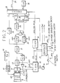
- FIG. 2 is a block diagram showing the arrangement of a video camera section;
- FIG. 3 is a schematic diagram showing the arrangement of a zoom driver;
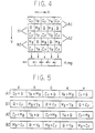
- FIG. 4 is a diagram showing color coding of an imaging device;
- FIG. 5 is a diagram showing an output of a horizontal output register of the imaging device;
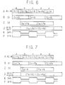
- FIG. 6 is a diagram illustrating a chrominance signal processing;
- FIG. 7 is a diagram also illustrating the chrominance signal processing;
- FIG. 8 is a wiring diagram showing the arrangement of a shutter system;
- FIG. 9 is a wiring diagram also showing the arrangement of the shutter system;
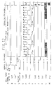
- FIG. 10 is a timing chart showing an operation of the shutter system;
- FIG. 11 is a wiring diagram showing the arrangement of a self-timer controller;
- FIG. 12 is a timing chart showing a shutter operation by a self-timer;
- FIG. 13 is a timing chart also showing a shutter operation by the self-timer;
- FIG. 14 is a block diagram showing an example of the arrangement of a shutter system for a still video camera;
- One embodiment of the present invention will be described with reference to the drawings. In this embodiment, a video camera and a photographic camera are integrally combined.
- FIG. 1 is a perspective view showing an external appearance of the embodiment, wherein
reference numeral 1 denotes a cabinet which has a built-in video camera section including an imaging device, a signal processing circuit, etc., and a built-in photographic camera section including a film loading mechanism, a film drive mechanism, etc., none of which are shown. -
Reference numeral 2 denotes an imaging lens of the video camera section, and 3 denotes an imaging lens of the photographic camera section. Namely, an optical system for the video camera section is separate from that for the photographic camera section. A 6-power zoom lens having a focal length f of 7 to 42 mm is used for theimaging lens 2, and a fixed-focus lens having a focal length f of 55 mm is used for theimaging lens 3. - In this embodiment, an electronic viewfinder comprising a small-sized CRT is arranged in the
cabinet 1, for displaying on the CRT an image picked up by the video camera section through theimaging lens 2.Reference numeral 4 represents an eyecup. There is provided no finder permitting a direct observation of an image to be photographed by the photographic camera section through theimaging lens 3. - Further, 5T and 5W denote zoom buttons for a Zooming operation in a TELE direction and a WIDE direction, respectively, 6 denotes a record button for recording a video signal output from the video camera section in a VTR, 7 denotes a shutter button, and 8 denotes a film rewind button.
- FIG. 2 shows the arrangement of the video camera section. An image light from an object enters through the
imaging lens 2 and aniris 11 and falls upon a single-plate CCD solid-state imaging device 12 having a complementary checkered color filter. - The zooming power of the
imaging lens 2 is adjusted by azoom driver 41. FIG. 3 shows in detail the arrangement of thezoom driver 41. whereinreference numeral 411 denotes a lens forming theimaging lens 2 for adjusting the zooming power. Thelens 411 can be moved back and forth when rotated, whereby the zooming power is adjusted. For example, if thelens 411 is rotated in a direction T, the zooming power changes in the TELE direction; if the lens is rotated in a direction W, the zooming power changes in the WIDE direction. - The
lens 411 is rotated by aDC motor 412, which has both ends connected to output terminals q1 and q2 of azoom driver unit 413, respectively. Input terminals p1 and p2 of thezoom driver unit 413 are respectively connected to fixed terminals T and W of azoom switch 42. - In this arrangement, when a high-level "H" signal is supplied to the terminal p1, a current flows through the
motor 412 from the terminal q1 to the terminal q2 (as indicated by the solid line), and thelens 411 is rotated in the direction T. On the other hand, when a high-level "H" signal is supplied to the terminal p2, a current flows through themotor 412 from the terminal q2 to the terminal q1 (as indicated by the dashed line), and thelens 411 is rotated in the direction W. When neither the terminal p1 nor the terminal p2 is supplied with a high-level "H" signal, no current flows through themotor 412, and accordingly, thelens 411 is not rotated in either direction and the position thereof is maintained. - A movable terminal of the
zoom switch 42 is connected to a power supply terminal. When theoperating button aforementioned cabinet 1 is pressed, thezoom switch 42 is connected to the terminal T or W, and a high-level "H" signal is supplied to the terminal p1 or p2 of thezoom driver unit 413, whereby the zooming power is adjusted in the TELE or WIDE direction. - FIG. 4 is a schematic diagram showing color coding of the
imaging device 12, and as illustrated, a field readout is carried out. In A field, charges are mixed in pairs, such as a pair of A1 and A2, and in B field, charges are mixed in pairs, such as a pair of B1 and B2. For the A field, charges are output in order of A1, A2, ..., and for the B field in order of B1, B2, ..., from a horizontal shift register Hreg. - As shown in FIG. 4, the order of charges a, b, ... is (Cy + G), (Ye + Mg), ... in A1 line, (Cy + Mg), (Ye + G), ... in A2 line, (G + Cy), (Mg + Ye), ... in B1 line, and (Mg + Cy); (G + Ye), ... in B2 line.
- The output signal of the
imaging device 12 is supplied to a CDS circuit (correlation double sampling circuit) 13 and is extracted thereby as an image signal. By using theCDS circuit 13, it is possible to reduce reset noise, as is known in the art. - Timing pulses needed by the
imaging device 12 and theCDS circuit 13 are produced by atiming generator 14. Thetiming generator 14 is supplied with reference clock pulses CK0 at 8 fsc (fsc represents the color subcarrier frequency) from anoscillator 15, as well as horizontal and vertical synchronizing signals HD and VD from asynchronizing generator 16. Thesynchronizing generator 16 is supplied with clock pulses CK1 at 4 fsc from thetiming generator 14. - An image signal output from the
CDS circuit 13 is supplied to alevel detecting circuit 17, which outputs a signal to aniris driver 18. Theiris driver 18 automatically controls the aperture of theiris 11. - A process for obtaining a luminance signal Y and a chroma signal (color differential signal) from the image signal output from the
CDS circuit 13 will be explained. - The luminance signal Y is obtained by adding adjacent signals together. Namely, referring to FIG. 5, summation signals are derived in sequence of a + b, b + c, c + d, d + e, ....
- For example, the A1 line can be approximated as shown in the following equation:

- The A2 line can be approximated as follows:

- The other lines in the A filed and the lines in the B field can be approximated in a similar manner.
- The chroma signal is obtained by subjecting adjacent signals to a subtraction.
- For example, the A1 line can be approximated as shown in the following equation:

- The A2 line can be approximated as follows:

- Similarly, for the other lines in the A field and the lines in the B field, a red differential signal R - Y and a blue differential signal -(B - Y) are alternately derived in a line sequential manner.
- Referring again to FIG. 2, the image signal output from the
CDS circuit 13 is supplied to a low-pass filter 20 constituting a luminance processing unit through anAGC circuit 19. The low-pass filter 20 carries out an addition (averaging) of adjacent signals, and accordingly, a luminance signal Y is output therefrom. - The image signal output from the
AGC circuit 19 is supplied to sample holdingcircuits sample holding circuits timing generator 14. In FIG. 6, A shows the signal of the A1 line, and in FIG. 7, A shows the signal of the A2 line. - The
sample holding circuit 21 outputs a continuous signal S1 of (Cy + G) or (Cy + Mg) to a subtracter 23 (see B in FIGS. 6 and 7), and thesample holding circuit 22 outputs a continuous signal S2 of (Ye + Mg) or (Ye + G) to the subtracter 23 (see C in FIGS. 6 and 7). - The
subtracter 23 subtracts the signal S1 from the signal S2, whereby a red differential signal R - Y and a blue differential signal -(B - Y) are alternately output therefrom in a line sequential manner (as indicated at D in FIGS. 6 and 7). - The color differential signals output from the
subtracter 23 are supplied directly to a fixed terminal b of achangeover switch 24 and a fixed terminal a of achangeover switch 25, and also supplied to a fixed terminal a of thechangeover switch 24 and a fixed terminal b of thechangeover switch 25 via adelay circuit 26 having a delay time corresponding to one horizontal period. - The switching operation of the changeover switches 24 and 25 is controlled by a
controller 27. Specifically, the switches are connected to the respective terminals b during a horizontal period in which the red differential signal R - Y is output from thesubtracter 23, and connected to the respective terminals a during a horizontal period in which the blue differential signal -(B - Y) is output. Thecontroller 27 is supplied with the synchronizing signals HD and VD as reference synchronizing signals from the synchronizinggenerator 16, and the clock pulses CK1 from thetiming generator 14. - Since the changeover switches 24 and 25 are operated in the above-described manner, a red differential signal R - Y is output from the
changeover switch 24 in each horizontal period and a blue differential signal -(B - Y) is output from thechangeover switch 25 in each horizontal period. - The luminance signal Y output from the low-
pass filter 20 and the color differential signals (R - Y) and -(B - Y) output from the changeover switches 24 and 25 are supplied to anencoder 28. Theencoder 28 is further supplied with a composite synchronizing signal SYNC, a blanking signal BLK, a burst flag signal BF, and a color subcarrier signal SC from the synchronizinggenerator 16. - In the
encoder 28, as is conventionally known, the luminance signal Y is combined with the synchronizing signal SYNC, and the color differential signals are subjected to quadrature two-phase modulation to form a carrier chrominance signal C and further combined with a color burst signal. The luminance signal Y and the carrier chrominance signal C are added together to form a color video signal SCV according to, e.g., the NTSC system. - The color video signal SCV thus generated by the
encoder 28 appears at anoutput terminal 29. Theencoder 28 also generates a monochromatic video signal SV (i.e., the luminance signal Y combined with the synchronizing signal SYNC), which is supplied to anelectronic viewfinder 30, and thus the acquired image is displayed at the small-sized CRT. - The
controller 27 is connected to ashutter switch 32 which turns on when theshutter button 7 is pressed, arecord switch 34 which turns on when therecord button 6 is pressed, a self-timer standby switch 33, and amode changeover switch 35 for switching between a still mode for acquiring a still image and a video mode for acquiring a dynamic image. The still mode is set when themode changeover switch 35 is connected to a terminal s, and the video mode is set when theswitch 35 is connected to a terminal v. - While in the still mode, if the
shutter switch 32 is turned on when thestandby switch 33 is off, thecontroller 27 immediately outputs a shutter pulse PSH and a record pulse PREC. On the other hand, while in the still mode, if theshutter switch 32 is turned on after thestandby switch 33 is turned on, thecontroller 27 outputs a shutter pulse PSH and a record pulse PREC upon lapse of a predetermined time, whereby a self-timer function is achieved. - The shutter pulse PSH is used to actuate the mechanical shutter of the photographic camera section (not shown), and the record pulse PREC is used to transfer a still image video signal to a still image recorder (not shown). For the still image recorder, a recorder using a DAT, which the applicant proposed before (Unexamined Japanese Patent Publication No. 2-161661), may be used.
- While in the video mode, if the
record switch 34 is turned on, thecontroller 27 immediately outputs a record pulse PREC. This record pulse PREC is used to control the recording operation of a recorder such as a VTR. Further, when theshutter switch 32 is turned on in the video mode, thecontroller 27 immediately outputs a shutter pulse PSH. This shutter pulse PSH is used to actuate the mechanical shutter of the photographic camera section, as in the still mode described above. - FIGS. 8 and 9 show the arrangement of a shutter system (shutter pulse generating unit) of the
controller 27. - As shown in FIG. 8, a series circuit composed of the self-
timer standby switch 33 and aresistor 39 has one end connected to a power supply and the other end grounded, and a signal S33 obtained at the node P3 between thestandby switch 33 and theresistor 39 is supplied to a self-timer controller 51. In this arrangement, a self-timer mode is established when thestandby switch 33 is turned on during a normal shutter mode, and the normal shutter mode is established when thestandby switch 33 is turned on during the self-timer mode. - The
controller 51 outputs a signal S51a which is low-level "L" in the normal shutter mode and is high-level "H" in the self-timer mode, and also outputs signals S51b and S51e which are high-level "H" in the normal shutter mode and low-level "L" in the self-timer mode. - When the
shutter switch 32 is turned on in the self-timer mode, a count mode is set for a timer count period, and upon lapse of the timer count period, the normal shutter mode is automatically restored, as described later. Thecontroller 51 further outputs a signal S51f which is high-level "H" during the timer count period and is low-level "L" during a period other than the timer count period, and a signal S51c which is set to high level "H" for a predetermined period subsequent to the timer count period. - The
controller 51 is supplied with a signal S68c, which is obtained by subjecting the vertical synchronizing signal VD (frequency: fv) to a frequency division of 1/128 at afrequency divider 68, mentioned later, as reference clock pulses for the timer. - A series circuit composed of the
shutter switch 32 and aresistor 52 is connected at one end to the power supply and grounded at the other end, and the node P1 between theshutter switch 32 and theresistor 52 is connected to one input terminal of anOR circuit 53. To the other input terminal of theOR circuit 53 is supplied the signal S51c output from thecontroller 51. - The output signal of the
OR circuit 53 is supplied to one input terminal of an ANDcircuit 54, and the signal S51b output from thecontroller 51 is supplied to the other input terminal of the ANDcircuit 54. The node P1 is connected to one input terminal of an ANDcircuit 55, the other input terminal of which is supplied with the signal S51a output from thecontroller 51. The output signal S55 of the ANDcircuit 55 is supplied to thecontroller 51. - The output signal S54 of the AND
circuit 54 is supplied to one input terminal of an ANDcircuit 56 and also to an integrating circuit composed of aresistor 57 and acapacitor 58. The output signal S54' of the integrating circuit is supplied to the other input terminal of the ANDcircuit 56 through aninverter 59, and the ANDcircuit 56 outputs a shutter signal S56. - Another series circuit composed of the
record switch 34 and aresistor 60 is connected at one end to the power supply and grounded at the other end, and the node P2 between therecord switch 34 and theresistor 60 is connected to one input terminal of aNAND circuit 62 through aninverter 61. The output signal of theinverter 61 is supplied to an integrating circuit composed of aresistor 63 and acapacitor 64, and the output signal of the integrating circuit is supplied to the other input terminal of theNAND circuit 62 through aninverter 65. The output signal of theNAND circuit 62 is supplied to one input terminal of an ANDcircuit 66. - The fixed terminal v of the
mode changeover switch 35 is connected to the power supply, while the fixed terminal s of the same switch is grounded, and a signal S35 output from the movable terminal of theswitch 35 is supplied to the other input terminal of the ANDcircuit 66. The ANDcircuit 66 outputs a record signal S66. - As shown in FIG. 9, the shutter signal S56 and the record signal S66, output respectively from the AND
circuits OR circuit 67, which then outputs a signal S67 to theaforesaid frequency divider 68. Thefrequency divider 68 is also supplied with the vertical synchronizing signal VD as a frequency-divided signal. Thefrequency divider 68 outputs a signal S68a obtained through a frequency division of 1/2, a signal S68b obtained through a frequency division of 1/64, and the aforesaid signal S68c obtained through a frequency division of 1/128. The signal S68c is supplied to thecontroller 51 as the reference clock pulses for the timer, as mentioned above. Thefrequency divider 68 is designed to carry out the frequency division when the output signal S67 of theOR circuit 67 is high-level "H" and not to carry out the frequency division when the signal S67 is low-level "L." - The OR
circuit 67 is supplied with the signals S51f and S68b output from thecontroller 51 and thefrequency divider 68, respectively, in addition to the aforesaid signals S56 and S66. - The signal S68b output from the
frequency divider 68 is supplied to one input terminal of aNAND circuit 69 through aninverter 72, and also to an integrating circuit formed by a series circuit including aresistor 70 and acapacitor 71. The output signal of the integrating circuit is supplied to the other input terminal of theNAND circuit 69. - The output signal of the
NAND circuit 69 is supplied to one input terminal of an ANDcircuit 73, the other input terminal of which is supplied with the output signal S35 of themode changeover switch 35. The output signal S73 of the ANDcircuit 73 is supplied to the clear terminal (CLR bar) and preset terminal (PR bar) of each of J-K flip-flops - The J and K terminals of each of the flip-
flops flops inverters - A signal S74 output from the noninverting output terminal Q of the flip-
flop 74 is supplied to an ANDcircuit 78. The ANDcircuit 78 is also supplied with the signals S68a and S51e output from thefrequency divider 68 and thecontroller 51, respectively. The ANDcircuit 78 outputs the shutter pulse PSH, as described later. - A signal S75 output from the noninverting output terminal Q of the flip-
flop 75 is supplied to an ANDcircuit 79, which is also supplied with the signals S68b and S51e output from thefrequency divider 68 and thecontroller 51, respectively. The output signal of the ANDcircuit 79 is supplied to the D terminal of a D flip-flop 80. The clock terminal CK of the flip-flop 80 is supplied with the vertical synchronizing signal VD. - A signal output from the noninverting output terminal Q of the flip-
flop 80 is supplied to one input terminal of an ANDcircuit 81, and also to an integrating circuit formed by a series circuit including aresistor 82 and acapacitor 83. The output signal of the integrating circuit is supplied to the other input terminal of the ANDcircuit 81. The ANDcircuit 81 outputs the record pulse PREC, as described later. - In the above-described arrangement, when the normal shutter mode is set during the still mode in which the
mode changeover switch 35 is connected to the terminal s, the output signal S35 of themode changeover switch 35 turns low "L" (shown in FIG. 10B) while the signal S51e output from thecontroller 51 is high-level "H" (shown in FIG. 10A). - While in this state, if the
shutter switch 32 is turned on, the output signal S54 of the ANDcircuit 54 becomes high-level "H" during the "on" period for which theswitch 32 remains in an on state (see FIG. 10C). In this case, the integrating circuit composed of theresistor 57 and thecapacitor 58 outputs a signal S54' having a waveform as indicated by the dashed line in FIG. 10C, and accordingly, when theshutter switch 32 is turned on, the shutter signal S56 becomes high-level "H" (FIG. 10E) and theinverter 77 outputs a signal S77 as shown in FIG. 10M. - In response to the rise to high level "H" of the shutter signal S56, the output signal of the
OR circuit 67 becomes high-level "H," and accordingly, thefrequency divider 68 starts counting and outputs the signals S68a and S68b (indicated at G and H in FIG. 10). - Since, in the still mode, the output signal S35 of the
mode changeover switch 35 is low-level "L," the output signal S73 of the ANDcircuit 73 is low-level "L" (FIG. 10I). The signals S74 and S75 output from the noninverting output terminals Q of the respective flip-flops - Therefore, the AND
circuit 78 outputs a high-level "H" shutter pulse PSH (FIG. 10L) immediately theshutter switch 32 is turned on. The noninverting output terminal Q of the flip-flop 80 outputs a signal S80 as shown in FIG. 100, and therefore, the ANDcircuit 81 outputs a high-level "H" record pulse PREC (FIG. 10P) immediately theshutter switch 32 is turned on. - Since, in the still mode, the output signal S35 of the
mode changeover switch 35 is low-level "L," the record signal S66 does not turn to high level "H" (FIG. 10F) even when therecord switch 34 is turned on (FIG. 10D). Accordingly, even if therecord switch 34 is turned on, neither the shutter pulse PSH nor the record pulse PREC is output. - When the self-timer mode is set during the still mode in which the
mode changeover switch 35 is connected to the terminal s, the output signal S35 of themode changeover switch 35 is low-level "L" (FIG. 10B) and the signal S51e output from thecontroller 51 becomes low-level "L" (FIG. 10A). - While in this state, if the
shutter switch 32 is turned on, the output signal S54 of the ANDcircuit 54 becomes high-level "H" during the "on" period for which theswitch 32 remains on (shown in FIG. 10C). In this case, the integrating circuit composed of theresistor 57 and thecapacitor 58 outputs a signal S54' having a waveform as indicated by the dashed line in FIG. 10C, and accordingly, when theshutter switch 32 is turned on, the shutter signal S56 becomes high-level "H" (FIG. 10E) and theinverter 77 outputs a signal S77 as shown in FIG. 10M. - In response to the rise to high level "H" of the shutter signal S56, the output signal of the
OR circuit 67 becomes high-level "H" and accordingly, thefrequency divider 68 starts counting. Since the signal S51f output from thecontroller 51 remains high-level "H" during the timer count period, the signals S68a and S68b are output from thefrequency divider 68 over the timer count period (indicated at G and H in FIG. 10). - Since, in the still mode, the output signal S35 of the
mode changeover switch 35 is low-level "L," the output signal S73 of the ANDcircuit 73 is low-level "L" (shown in FIG. 10I). The signals S74 and S75 output from the noninverting output terminals Q of the respective flip-flops controller 51 is low-level "L" (FIG. 10A), the shutter pulse PSH and the record pulse PREC are not immediately output if theshutter switch 32 is turned on, unlike the normal shutter mode described above. - When the timer count period has passed, the self-timer mode switches to the normal shutter mode. Immediately after the timer count period ends, the signal S51c output from the
controller 51 turns to high-level "H" for a predetermined period, whereby the output signal S54 of the ANDcircuit 54 becomes high-level "H" (see FIG. 10C). Accordingly, the shutter signal S56 becomes high-level "H" (FIG. 10E) upon lapse of the timer count period. - In response to the rise to high level "H" of the shutter signal S56, the output signal of the
OR circuit 67 becomes high-level "H," and accordingly, thefrequency divider 68 starts counting and outputs the signals S68a and S68b (indicated at G and H in FIG. 10). - Since, in the still mode, the output signal S35 of the
mode changeover switch 35 is low-level "L," the output signal S73 of the ANDcircuit 73 is low-level "L" (FIG. 10I), and the signals S74 and S75 output from the noninverting output terminals Q of the respective flip-flops controller 51 is high-level "H" (FIG. 10A). Therefore, immediately after the timer count period has passed, a high-level "H" shutter pulse PSH is output from the AND circuit 78 (FIG. 10L) and a high-level "H" record pulse PREC is output from the AND circuit 81 (FIG. 10P). - In the video mode in which the
mode changeover switch 35 is connected to the terminal v, the output signal S35 of themode changeover switch 35 is high-level "H" (FIG. 10B), and in the normal shutter mode, the signal S51e output from thecontroller 51 is high-level "H" (FIG. 10A). - While in this state, if the
shutter switch 32 is turned on, the output signal S54 of the ANDcircuit 54 becomes high-level "H" during the "on" period for which theswitch 32 remains on (shown in FIG. 10C). In this case, the integrating circuit composed of theresistor 57 and thecapacitor 58 outputs a signal S54' having a waveform as indicated by the dashed line in FIG. 10C, and accordingly, when theshutter switch 32 is turned on, the shutter signal S56 becomes high-level "H" (FIG. 10E) and theinverter 77 outputs a signal S77 as shown in FIG. 10M. - In response to the rise to high level "H" of the shutter signal S56, the output signal of the
OR circuit 67 becomes high-level "H," and accordingly, thefrequency divider 68 starts counting and outputs the signals S68a and S68b (indicated at G and H in FIG. 10). - Since, in the video mode, the output signal S35 of the
mode changeover switch 35 is high-level "H," the output signal S73 of the ANDcircuit 73 becomes high-level "H" (shown in FIG. 10I) corresponding to the rise to high level "H" of the shutter signal S56. In this case, since the record signal S66 remains low-level "L" and thus the output signal S76 of theinverter 76 remains high-level "H" (shown in FIG. 10J), the output signal S74 from the noninverting output terminal Q of the flip-flop 74 remains high-level "H" (see FIG. 10K). Therefore, a high-level "H" shutter pulse PSH is output from the AND circuit 78 (FIG. 10L) immediately theshutter switch 32 is turned on. - In response to the rise to high level "H" of the shutter signal S56, the output signal S77 of the
inverter 77 becomes low-level "L" (FIG. 10M) and the output signal S75 from the noninverting output terminal Q of the flip-flop 75 becomes low-level "L" (FIG. 10N). Accordingly, even if theshutter switch 32 is turned on, the ANDcircuit 81 does not output a high-level "H" record pulse PREC (shown in FIG. 10P). - When the
record switch 34 is turned on (see FIG. 10D) in the video mode, the record signal S66 output from the ANDcircuit 66 becomes high-level "H" (FIG. 10F) because the output signal S35 of themode changeover switch 35 is high-level "H" (FIG. 10B), and therefore, theinverter 76 outputs a signal S76 as shown in FIG. 10J. - In response to the rise to high level "H" of the record signal S66, the output signal of the
OR circuit 67 becomes high-level "H," and accordingly, thefrequency divider 68 starts counting and outputs the signals S68a and S68b (indicated at G and H in FIG. 10). - Since, in the video mode, the output signal S35 of the
mode changeover switch 35 is high-level "H," the output signal S73 of the ANDcircuit 73 becomes high-level "H" (shown in FIG. 10I) corresponding to the rise to high level "H" of the record signal S66. In this case, since the shutter signal S56 remains low-level "L" and thus the output signal S77 of theinverter 77 remains high-level "H" (see FIG. 10M), the output signal S75 from the noninverting output terminal Q of the flip-flop 75 remains high-level "H" (see FIG. 10N). Therefore, a high-level "H" record pulse PREC is output from the AND circuit 81 (FIG. 10P) immediately therecord switch 34 is turned on. - In response to the rise to high level "H" of the record signal S66, the output signal S76 of the
inverter 76 becomes low-level "L" (see FIG. 10J) and the output signal S74 from the noninverting output terminal Q of the flip-flop 74 becomes low-level "L" (FIG. 10K). Accordingly, even if therecord switch 34 is turned on, the ANDcircuit 78 does not output a high-level "H" shutter pulse PSH (FIG. 10L). - Although not described in detail, the self-timer mode can be set also in the video mode, by operating the
standby switch 33. In this case, if theshutter switch 32 is turned on, the ANDcircuit 78 outputs a high-level "H" shutter pulse PSH upon lapse of the timer count period. - FIG. 11 shows the arrangement of the self-
timer controller 51 in detail. As shown in the figure, the output signal of the ANDcircuit 55 is inverted and applied to the clock terminal CK of a J-K flip-flop 85. The flip-flop 85 is supplied with a high-level "H" signal at each of the J and K terminals thereof, and thus is set to perform a flip-flop action. A high-level "H" signal is also supplied to the preset terminal (PR bar) of the flip-flop 85. A signal S85 appearing at the noninverting output terminal Q of the flip-flop 85 is output as the signal S51f and also supplied to aninput terminal 1 of ashift register 86. - When a low-level "L" signal is supplied to the clear terminal (CLR bar) or
input terminal 2 of theshift register 86, theshift register 86 is cleared. When a high-level "H" signal is supplied to both the clear terminal (CLR bar) andinput terminal 2 of theshift register 86, the signal supplied to theinput terminal 1 is shifted successively to output terminals A-F and output in synchronism with the clock pulse. - The signal S33 obtained at the node P3 between the
standby switch 33 and theresistor 39 is inverted and applied to the clock terminal CK of a J-K flip-flop 87. The flip-flop 87 is supplied with a high-level "H" signal at each of the J and K terminals thereof, and thus is set to perform a flip-flop action. A high-level "H" signal is also supplied to the preset terminal (PR bar) of the flip-flop 87. - A signal S87 appearing at the noninverting output terminal Q of the flip-
flop 87 is output as the signal S51a and also supplied to the clear terminal (CLR bar) of the flip-flop 85 and theinput terminal 2 of theshift register 86. A signal S87' appearing at the inverting output terminal (Q bar) of the flip-flop 87 is output as the signals S51b and S51e. - The output signal S55 of the AND
circuit 55 is supplied to one input terminal of an ANDcircuit 89 through aninverter 88, and the output signal S89 of the ANDcircuit 89 is supplied to the clear terminal (CLR bar) of theshift register 86. A signal Sof output from the output terminal F of theshift register 86 is supplied to the clear terminal (CLR bar) of the flip-flop 87 through aninverter 92. Further, the output signal Sof is supplied to the other input terminal of the ANDcircuit 89 through aninverter 90 having a hysteresis characteristic, and is also output as the signal S51c through a series circuit composed of theinverters - The signal S68c output from the
frequency divider 68 is supplied to the clock terminal CK of theshift register 86. - The shutter operation carried out by the self-timer will be now described in detail with reference to FIGS. 12 and 13.
- When the
standby switch 33 is released (turned off) after it is depressed (turned on) (see FIG. 12A), the signal S87 output from the noninverting output terminal Q of the flip-flop 87 changes from low "L" to high level "H," and at the same time, the signal S87' output from the inverting output terminal (Q bar) of the same flip-flop changes from high "H" to low level "L" (indicated at B and C in FIG. 12). Consequently, the mode is switched from the normal shutter mode to the self-timer mode. - While in the self-timer mode, if the
shutter switch 32 is once depressed (turned on) and thereafter released (turned off) (see FIG. 12D), the output signal S85 from the noninverting output terminal Q of the flip-flop 85 changes from low level "L" to high level "H" (see FIG. 12E), whereby the timer count period starts. - Upon start of the timer count period, the output signal S67 of the
OR circuit 67 turns to high level "H" (shown in FIG. 12K), and therefore, thefrequency divider 68 starts the frequency division. Consequently, the frequency-divided signals S68a to S68c are output from the frequency divider 68 (indicated at L, F and G in FIG. 12). - During the timer count period, a high-level "H" signal is supplied from the noninverting output terminal Q of the flip-
flop 87 to theinput terminal 2 of theshift register 86, a high-level "H" signal is supplied from the ANDcircuit 89 to the clear terminal (CLR bar) of theshift register 86, and a high-level "H" signal is supplied from the noninverting output terminal Q of the flip-flop 85 to theinput terminal 1 of the shift register. FIG. 12J shows the output signal S89 of the ANDcircuit 89. Accordingly, during the timer count period, theshift register 86 shifts data successively to the output terminals A-F and outputs a high-level "H" signal in a manner timed with the rise of the signal S68c output from the frequency divider 68 (see FIG. 12G). Symbols Soa to Sof in FIG. 12H denote the signals output from the terminals A-F, respectively. - In the timer count period, the zeroth to 671st vertical synchronizing signals VD are supplied, and when the 672nd vertical synchronizing signal VD is supplied, the output signal Sof changes from low "L" to high level "H" (see FIG. 12H), and a low-level "L" signal is supplied from the
inverter 92 to the clear terminal (CLR bar) of the flip-flop 87. Consequently, the signal S87 output from the noninverting output terminal Q of the flip-flop 87 changes from high "H" to low level "L" and at the same time the signal S87' output from the inverting output terminal (Q bar) of the same flip-flop changes from low "L" to high level "H" (indicated at B and C in FIG. 12), whereby the self-timer mode is ended. - At this time, since a low-level "L" signal is supplied from the noninverting output terminal Q of the flip-
flop 87 to theinput terminal 2 of theshift register 86, theshift register 86 is cleared and the signals Soa to Sof at the output terminals A to F become low-level "L" (shown in FIG. 12H). - Furthermore, a low-level "L" signal is supplied from the noninverting output terminal Q of the flip-
flop 87 to the clear terminal (CLR bar) of the flip-flop 85, and thus the signal S85 output from the noninverting output terminal Q of the flip-flop 85 changes from high "H" to low level "L" (see FIG. 12E). Accordingly, the output signal S67 of theOR circuit 67, which is supplied to thefrequency divider 68, becomes low-level "L" (shown in FIG. 12K), whereby the frequency division by thefrequency divider 68 is stopped and a low-level "L" signal appears at each of the frequency-divided signal output terminals (indicated at L, F and G in FIG. 12). - Since the
inverter 90 has a hysteresis characteristic as mentioned above, the output signal S90 thereof changes from high "H" to low level "L" (FIG. 12I) upon lapse of a predetermined period τ after the signal Sof output from the output terminal F of theshift register 86 has changed from low "L" to high level "H." Consequently, the output signal of the ANDcircuit 54 becomes high-level "H" and theoutput signal 67 of theOR circuit 67, which is supplied to thefrequency divider 68, becomes high-level "H" (shown in FIG. 12K), whereby thefrequency divider 68 restarts the frequency division. - During a period in which the zeroth to 31st vertical synchronizing signals VD are supplied after the restart of the frequency division by the
frequency divider 68, the output signal S68b of thefrequency divider 68 remains high-level "H" (shown in FIG. 12F) and the output signal S67 of theOR circuit 67 also remains high level "H," whereby the frequency division is continued (see FIG. 12K). However, when the 32nd vertical synchronizing signal VD is supplied, the output signal S68b of thefrequency divider 68 changes from high "H" to low level "L" (see FIG. 12F). Accordingly, the output signal S67 of theOR circuit 67 changes from high "H" to low level "L" (FIG. 12K), and the frequency division by thefrequency divider 68 is stopped. - The frequency-divided signal S68a is output from the frequency divider 68 (see FIG. 12L) during the period in which the frequency division is carried out (i.e., the timer count period plus subsequent 32 vertical periods). Since the signal S87' output from the inverting output terminal (Q bar) of the flip-
flop 87 turns high "H" at the end of the timer count period, the frequency-divided signal S68a output from thefrequency divider 68 during the 32 vertical periods following the timer count period is output from the ANDcircuit 78 as the shutter pulse PSH (see FIG. 12M). - In FIG. 13, A through G illustrate states of principal ones of the signals shown in FIG. 12 before and after the end of the timer count period along an enlarged time base.
- As mentioned above, when the
shutter switch 32 is turned on and then turned off during the self-timer mode, the shutter pulse PSH is output after the end of the timer count period (about 672 vertical periods, nearly equal to 11.2 sec). When the timer count period ends, the self-timer mode is automatically canceled and the normal shutter mode is restored. - According to this embodiment, in the still mode, the shutter pulse PSH and the record pulse PREC are output in response to an operation of the
shutter switch 32, and in the video mode, the record pulse PREC is output in response to an operation of therecord switch 34 and the shutter pulse PSH is output in response to an operation of theshutter switch 32. Therefore, the shutter pulse PSH and the record pulse PREC can be output appropriately in both the still mode and the video mode. - Further, in this embodiment, in both the normal shutter mode and the self-timer mode, the shutter pulse PSH synchronized with the vertical synchronizing signal VD can be obtained from the output signal S68a of the
frequency divider 68, by operating theshutter switch 32. Furthermore, during the timer count period in the self-timer mode, theshift register 86, and thus the timer, is driven by the output signal S68c of thefrequency divider 68. Since thefrequency divider 68 is thus used for different purposes, the circuitry of the shutter system can be simplified, compared with that in a conventional system. - It will be obvious to those having ordinary skill in the art that many changes may be made in the above-described details of the preferred embodiments of the present invention without departing from the scope of the present invention.
Claims (5)
- A camera apparatus having a self-timer function and an exposure time function, comprising:
a frequency divider (68) for carrying out a frequency division with respect to a vertical synchronizing signal (VD), characterized in that an output signal (S68c) of the frequency divider being used to drive a timer (51) associated with the self-timer function and to obtain a shutter pulse (PSH). - The camera apparatus according to claim 1, wherein the timer (51) associated with the self-timer function comprises a shift register (86), the output signal of the frequency divider (68) being supplied as a shift clock pulse.
- The camera apparatus according to claim 1, which further comprises a shutter switch (32) and a self-timer standby switch (33), and wherein the self-timer standby switch (33) is operated to change a mode from a normal shutter mode to a self-timer mode, and a timer count period is set when the shutter switch (32) is operated in the self-timer mode.
- The camera apparatus according to claim 3, wherein, during the timer count period, the timer (51) associated with the timer function is driven by the output signal of the frequency divider (68), and the shutter mode is restored upon lapse of a fixed period.
- The camera apparatus according to claim 4, wherein the frequency divider (68) is operated for a predetermined period after the shutter mode is restored, such that the output signal of the frecuency divider (68) is gated to obtain the shutter pulse.
Priority Applications (2)
| Application Number | Priority Date | Filing Date | Title |
|---|---|---|---|
| EP95118088A EP0726507B1 (en) | 1991-08-30 | 1992-08-26 | An aspect conversion circuit used in a camera apparatus |
| EP95118089A EP0709753B1 (en) | 1991-08-30 | 1992-08-26 | A camera apparatus comprising a video camera and a photographic camera |
Applications Claiming Priority (12)
| Application Number | Priority Date | Filing Date | Title |
|---|---|---|---|
| JP219748/91 | 1991-08-30 | ||
| JP03219748A JP3080445B2 (en) | 1991-08-30 | 1991-08-30 | Camera device |
| JP03247786A JP3124585B2 (en) | 1991-09-26 | 1991-09-26 | Aspect conversion circuit |
| JP247786/91 | 1991-09-26 | ||
| JP4066358A JPH05276422A (en) | 1992-03-24 | 1992-03-24 | Longitudinal/lateral converting circuit |
| JP4066357A JPH05276421A (en) | 1992-03-24 | 1992-03-24 | Longitudinal/lateral converting circuit |
| JP66358/92 | 1992-03-24 | ||
| JP66357/92 | 1992-03-24 | ||
| JP133994/92 | 1992-05-26 | ||
| JP13399492A JP3251052B2 (en) | 1992-05-26 | 1992-05-26 | Aspect conversion circuit |
| JP173445/92 | 1992-06-30 | ||
| JP4173445A JPH0622202A (en) | 1992-06-30 | 1992-06-30 | Camera device |
Related Child Applications (4)
| Application Number | Title | Priority Date | Filing Date |
|---|---|---|---|
| EP95118088.4 Division-Into | 1992-08-26 | ||
| EP95118089A Division EP0709753B1 (en) | 1991-08-30 | 1992-08-26 | A camera apparatus comprising a video camera and a photographic camera |
| EP95118088A Division EP0726507B1 (en) | 1991-08-30 | 1992-08-26 | An aspect conversion circuit used in a camera apparatus |
| EP95118089.2 Division-Into | 1992-08-26 |
Publications (3)
| Publication Number | Publication Date |
|---|---|
| EP0529612A2 EP0529612A2 (en) | 1993-03-03 |
| EP0529612A3 EP0529612A3 (en) | 1993-05-05 |
| EP0529612B1 true EP0529612B1 (en) | 1996-12-04 |
Family
ID=27551042
Family Applications (3)
| Application Number | Title | Priority Date | Filing Date |
|---|---|---|---|
| EP95118089A Expired - Lifetime EP0709753B1 (en) | 1991-08-30 | 1992-08-26 | A camera apparatus comprising a video camera and a photographic camera |
| EP95118088A Expired - Lifetime EP0726507B1 (en) | 1991-08-30 | 1992-08-26 | An aspect conversion circuit used in a camera apparatus |
| EP92114565A Expired - Lifetime EP0529612B1 (en) | 1991-08-30 | 1992-08-26 | A camera apparatus having self timer function |
Family Applications Before (2)
| Application Number | Title | Priority Date | Filing Date |
|---|---|---|---|
| EP95118089A Expired - Lifetime EP0709753B1 (en) | 1991-08-30 | 1992-08-26 | A camera apparatus comprising a video camera and a photographic camera |
| EP95118088A Expired - Lifetime EP0726507B1 (en) | 1991-08-30 | 1992-08-26 | An aspect conversion circuit used in a camera apparatus |
Country Status (4)
| Country | Link |
|---|---|
| US (1) | US5592220A (en) |
| EP (3) | EP0709753B1 (en) |
| CA (1) | CA2076742A1 (en) |
| DE (3) | DE69215607T2 (en) |
Cited By (1)
| Publication number | Priority date | Publication date | Assignee | Title |
|---|---|---|---|---|
| RU2733274C1 (en) * | 2018-11-15 | 2020-10-01 | Кэнон Кабусики Кайся | Electronic device, control method for electronic device and computer-readable medium |
Families Citing this family (9)
| Publication number | Priority date | Publication date | Assignee | Title |
|---|---|---|---|---|
| JP3834130B2 (en) * | 1996-07-19 | 2006-10-18 | 株式会社リコー | Digital camera |
| JPH1079910A (en) * | 1996-09-05 | 1998-03-24 | Sony Corp | VTR integrated camera device |
| JPH10224690A (en) * | 1996-12-06 | 1998-08-21 | Nikon Corp | Information processing device and recording medium |
| US6842768B1 (en) | 2000-03-01 | 2005-01-11 | Siemens Communications, Inc. | Apparatus and method for selectable compression |
| JP2003069959A (en) * | 2001-06-14 | 2003-03-07 | Sony Corp | Video signal processing circuit, video signal processing method, and image display device |
| US20090244320A1 (en) * | 2005-08-26 | 2009-10-01 | Daisuke Ito | Imaging device, display control device, and display device |
| KR101258723B1 (en) | 2005-10-26 | 2013-04-26 | 파나소닉 주식회사 | Video reproducing device, video recorder, video reproducing method, video recording method, and semiconductor integrated circuit |
| EP2073532A1 (en) * | 2007-12-17 | 2009-06-24 | Koninklijke Philips Electronics N.V. | Video signal processing |
| CN109946709B (en) * | 2019-03-13 | 2021-03-26 | 维沃移动通信有限公司 | Image sensor, depth measurement method of terminal and terminal |
Citations (5)
| Publication number | Priority date | Publication date | Assignee | Title |
|---|---|---|---|---|
| EP0179672A1 (en) * | 1984-06-29 | 1986-04-30 | TEXAS INSTRUMENTS FRANCE Société dite: | Point processor for video images, related visualization system and method |
| DE3626532A1 (en) * | 1986-08-06 | 1988-02-11 | Siemens Ag | X-ray diagnosis device having a matrix of optoelectronic sensors |
| US4827348A (en) * | 1988-05-02 | 1989-05-02 | Polaroid Corporation | Exposure control system for dual mode electronic imaging camera |
| US4869237A (en) * | 1987-03-02 | 1989-09-26 | Olympus Optical Co., Ltd. | Electronic endoscope apparatus |
| GB2221116A (en) * | 1985-10-02 | 1990-01-24 | Olympus Optical Co | Endoscopic apparatus |
Family Cites Families (12)
| Publication number | Priority date | Publication date | Assignee | Title |
|---|---|---|---|---|
| CH918774A4 (en) * | 1974-07-04 | 1977-08-31 | ||
| JPH0241016B2 (en) * | 1980-06-05 | 1990-09-14 | Olympus Optical Co | KAMERANOSERUFUTAIMAASOCHI |
| DE3441025A1 (en) * | 1983-11-11 | 1985-05-30 | Canon K.K., Tokio/Tokyo | Video recording device |
| JPS6242132A (en) * | 1985-08-20 | 1987-02-24 | Asahi Optical Co Ltd | Shutter device of video camera |
| JPS62289073A (en) * | 1986-06-09 | 1987-12-15 | Sony Corp | Video printer |
| JP2507352B2 (en) * | 1986-09-30 | 1996-06-12 | 株式会社東芝 | Video system |
| JPS63281580A (en) * | 1987-05-13 | 1988-11-18 | Konica Corp | Still video camera |
| US4952967A (en) * | 1987-10-27 | 1990-08-28 | Canon Kabushiki Kaisha | Timer-assisted photographing mode control device for camera |
| JP2748003B2 (en) * | 1988-05-18 | 1998-05-06 | 京セラ株式会社 | Character pattern rotation processing method |
| JPH0232691A (en) * | 1988-07-22 | 1990-02-02 | Fuji Photo Film Co Ltd | Drive method for solid-state image pickup device |
| JPH0828060B2 (en) | 1988-12-14 | 1996-03-21 | アイワ株式会社 | Digital audio tape recorder |
| JP2920924B2 (en) * | 1989-01-12 | 1999-07-19 | ソニー株式会社 | CCD camera |
-
1992
- 1992-08-24 CA CA002076742A patent/CA2076742A1/en not_active Abandoned
- 1992-08-26 EP EP95118089A patent/EP0709753B1/en not_active Expired - Lifetime
- 1992-08-26 EP EP95118088A patent/EP0726507B1/en not_active Expired - Lifetime
- 1992-08-26 DE DE69215607T patent/DE69215607T2/en not_active Expired - Fee Related
- 1992-08-26 DE DE69228132T patent/DE69228132T2/en not_active Expired - Fee Related
- 1992-08-26 EP EP92114565A patent/EP0529612B1/en not_active Expired - Lifetime
- 1992-08-26 DE DE69231560T patent/DE69231560T2/en not_active Expired - Lifetime
-
1995
- 1995-02-14 US US08/390,802 patent/US5592220A/en not_active Expired - Lifetime
Patent Citations (5)
| Publication number | Priority date | Publication date | Assignee | Title |
|---|---|---|---|---|
| EP0179672A1 (en) * | 1984-06-29 | 1986-04-30 | TEXAS INSTRUMENTS FRANCE Société dite: | Point processor for video images, related visualization system and method |
| GB2221116A (en) * | 1985-10-02 | 1990-01-24 | Olympus Optical Co | Endoscopic apparatus |
| DE3626532A1 (en) * | 1986-08-06 | 1988-02-11 | Siemens Ag | X-ray diagnosis device having a matrix of optoelectronic sensors |
| US4869237A (en) * | 1987-03-02 | 1989-09-26 | Olympus Optical Co., Ltd. | Electronic endoscope apparatus |
| US4827348A (en) * | 1988-05-02 | 1989-05-02 | Polaroid Corporation | Exposure control system for dual mode electronic imaging camera |
Cited By (2)
| Publication number | Priority date | Publication date | Assignee | Title |
|---|---|---|---|---|
| RU2733274C1 (en) * | 2018-11-15 | 2020-10-01 | Кэнон Кабусики Кайся | Electronic device, control method for electronic device and computer-readable medium |
| US11044406B2 (en) | 2018-11-15 | 2021-06-22 | Canon Kabushiki Kaisha | Electronic apparatus capable of a notifying operation during countdown in self-timer shooting and control method thereof |
Also Published As
| Publication number | Publication date |
|---|---|
| DE69231560D1 (en) | 2000-12-14 |
| EP0726507B1 (en) | 2000-11-08 |
| EP0529612A3 (en) | 1993-05-05 |
| DE69215607T2 (en) | 1997-06-12 |
| EP0709753A1 (en) | 1996-05-01 |
| CA2076742A1 (en) | 1993-03-01 |
| DE69215607D1 (en) | 1997-01-16 |
| EP0709753B1 (en) | 1999-01-07 |
| DE69231560T2 (en) | 2001-05-31 |
| DE69228132D1 (en) | 1999-02-18 |
| DE69228132T2 (en) | 1999-07-22 |
| US5592220A (en) | 1997-01-07 |
| EP0529612A2 (en) | 1993-03-03 |
| EP0726507A1 (en) | 1996-08-14 |
Similar Documents
| Publication | Publication Date | Title |
|---|---|---|
| KR100246213B1 (en) | Imager | |
| EP0399232B1 (en) | Camera apparatus capable of freely setting objective area within viewed subject | |
| EP0709753B1 (en) | A camera apparatus comprising a video camera and a photographic camera | |
| EP0393710B1 (en) | Camera apparatus including automatic exposure control | |
| JPH0744653B2 (en) | Electronic still camera | |
| EP0518286B1 (en) | Video camera for camera system | |
| JP2002281375A (en) | Electronic camera and image display method in the case of automatic focus adjustment | |
| JPH0622202A (en) | Camera device | |
| JP3043834B2 (en) | Video camera | |
| JP3080445B2 (en) | Camera device | |
| JP3048437B2 (en) | Video camera | |
| JP3329475B2 (en) | Video camera | |
| JP3251031B2 (en) | Video camera equipment | |
| JPH05110915A (en) | Video camera | |
| JP3048410B2 (en) | Video camera | |
| JP3115653B2 (en) | Photo camera | |
| JP3214875B2 (en) | Camera device | |
| JP3043855B2 (en) | Camera device | |
| JP3048408B2 (en) | Video camera | |
| JP2001197359A (en) | Synchronism control method and image pickup device | |
| JP3048409B2 (en) | Video camera | |
| JP3048411B2 (en) | Video camera | |
| JP3048412B2 (en) | Video camera | |
| JP3043854B2 (en) | Camera device | |
| JPH05110916A (en) | Video camera |
Legal Events
| Date | Code | Title | Description |
|---|---|---|---|
| PUAI | Public reference made under article 153(3) epc to a published international application that has entered the european phase |
Free format text: ORIGINAL CODE: 0009012 |
|
| AK | Designated contracting states |
Kind code of ref document: A2 Designated state(s): BE DE FR GB IT NL |
|
| PUAL | Search report despatched |
Free format text: ORIGINAL CODE: 0009013 |
|
| AK | Designated contracting states |
Kind code of ref document: A3 Designated state(s): BE DE FR GB IT NL |
|
| 17P | Request for examination filed |
Effective date: 19931028 |
|
| 17Q | First examination report despatched |
Effective date: 19950529 |
|
| GRAG | Despatch of communication of intention to grant |
Free format text: ORIGINAL CODE: EPIDOS AGRA |
|
| GRAH | Despatch of communication of intention to grant a patent |
Free format text: ORIGINAL CODE: EPIDOS IGRA |
|
| GRAH | Despatch of communication of intention to grant a patent |
Free format text: ORIGINAL CODE: EPIDOS IGRA |
|
| GRAA | (expected) grant |
Free format text: ORIGINAL CODE: 0009210 |
|
| AK | Designated contracting states |
Kind code of ref document: B1 Designated state(s): BE DE FR GB IT NL |
|
| PG25 | Lapsed in a contracting state [announced via postgrant information from national office to epo] |
Ref country code: BE Effective date: 19961204 |
|
| XX | Miscellaneous (additional remarks) |
Free format text: TEILANMELDUNG 95118088.4 EINGEREICHT AM 16/11/95. |
|
| REF | Corresponds to: |
Ref document number: 69215607 Country of ref document: DE Date of ref document: 19970116 |
|
| ET | Fr: translation filed | ||
| ITF | It: translation for a ep patent filed | ||
| PLBE | No opposition filed within time limit |
Free format text: ORIGINAL CODE: 0009261 |
|
| 26N | No opposition filed | ||
| PGFP | Annual fee paid to national office [announced via postgrant information from national office to epo] |
Ref country code: NL Payment date: 20010827 Year of fee payment: 10 |
|
| REG | Reference to a national code |
Ref country code: GB Ref legal event code: IF02 |
|
| PG25 | Lapsed in a contracting state [announced via postgrant information from national office to epo] |
Ref country code: NL Free format text: LAPSE BECAUSE OF NON-PAYMENT OF DUE FEES Effective date: 20030301 |
|
| NLV4 | Nl: lapsed or anulled due to non-payment of the annual fee |
Effective date: 20030301 |
|
| PG25 | Lapsed in a contracting state [announced via postgrant information from national office to epo] |
Ref country code: IT Free format text: LAPSE BECAUSE OF NON-PAYMENT OF DUE FEES;WARNING: LAPSES OF ITALIAN PATENTS WITH EFFECTIVE DATE BEFORE 2007 MAY HAVE OCCURRED AT ANY TIME BEFORE 2007. THE CORRECT EFFECTIVE DATE MAY BE DIFFERENT FROM THE ONE RECORDED. Effective date: 20050826 |
|
| PGFP | Annual fee paid to national office [announced via postgrant information from national office to epo] |
Ref country code: DE Payment date: 20080912 Year of fee payment: 17 |
|
| PGFP | Annual fee paid to national office [announced via postgrant information from national office to epo] |
Ref country code: FR Payment date: 20080818 Year of fee payment: 17 |
|
| PGFP | Annual fee paid to national office [announced via postgrant information from national office to epo] |
Ref country code: GB Payment date: 20080903 Year of fee payment: 17 |
|
| GBPC | Gb: european patent ceased through non-payment of renewal fee |
Effective date: 20090826 |
|
| REG | Reference to a national code |
Ref country code: FR Ref legal event code: ST Effective date: 20100430 |
|
| PG25 | Lapsed in a contracting state [announced via postgrant information from national office to epo] |
Ref country code: FR Free format text: LAPSE BECAUSE OF NON-PAYMENT OF DUE FEES Effective date: 20090831 Ref country code: DE Free format text: LAPSE BECAUSE OF NON-PAYMENT OF DUE FEES Effective date: 20100302 |
|
| PG25 | Lapsed in a contracting state [announced via postgrant information from national office to epo] |
Ref country code: GB Free format text: LAPSE BECAUSE OF NON-PAYMENT OF DUE FEES Effective date: 20090826 |