EP0529605B1 - Méthode pour la limitation de courant d'un régulateur serie et son application - Google Patents
Méthode pour la limitation de courant d'un régulateur serie et son application Download PDFInfo
- Publication number
- EP0529605B1 EP0529605B1 EP92114532A EP92114532A EP0529605B1 EP 0529605 B1 EP0529605 B1 EP 0529605B1 EP 92114532 A EP92114532 A EP 92114532A EP 92114532 A EP92114532 A EP 92114532A EP 0529605 B1 EP0529605 B1 EP 0529605B1
- Authority
- EP
- European Patent Office
- Prior art keywords
- series regulator
- current
- power loss
- reaching
- control element
- Prior art date
- Legal status (The legal status is an assumption and is not a legal conclusion. Google has not performed a legal analysis and makes no representation as to the accuracy of the status listed.)
- Expired - Lifetime
Links
Images

Classifications
-
- H—ELECTRICITY
- H02—GENERATION; CONVERSION OR DISTRIBUTION OF ELECTRIC POWER
- H02H—EMERGENCY PROTECTIVE CIRCUIT ARRANGEMENTS
- H02H9/00—Emergency protective circuit arrangements for limiting excess current or voltage without disconnection
- H02H9/02—Emergency protective circuit arrangements for limiting excess current or voltage without disconnection responsive to excess current
- H02H9/025—Current limitation using field effect transistors
-
- G—PHYSICS
- G05—CONTROLLING; REGULATING
- G05F—SYSTEMS FOR REGULATING ELECTRIC OR MAGNETIC VARIABLES
- G05F1/00—Automatic systems in which deviations of an electric quantity from one or more predetermined values are detected at the output of the system and fed back to a device within the system to restore the detected quantity to its predetermined value or values, i.e. retroactive systems
- G05F1/10—Regulating voltage or current
- G05F1/46—Regulating voltage or current wherein the variable actually regulated by the final control device is dc
- G05F1/56—Regulating voltage or current wherein the variable actually regulated by the final control device is dc using semiconductor devices in series with the load as final control devices
- G05F1/565—Regulating voltage or current wherein the variable actually regulated by the final control device is dc using semiconductor devices in series with the load as final control devices sensing a condition of the system or its load in addition to means responsive to deviations in the output of the system, e.g. current, voltage, power factor
- G05F1/569—Regulating voltage or current wherein the variable actually regulated by the final control device is dc using semiconductor devices in series with the load as final control devices sensing a condition of the system or its load in addition to means responsive to deviations in the output of the system, e.g. current, voltage, power factor for protection
- G05F1/573—Regulating voltage or current wherein the variable actually regulated by the final control device is dc using semiconductor devices in series with the load as final control devices sensing a condition of the system or its load in addition to means responsive to deviations in the output of the system, e.g. current, voltage, power factor for protection with overcurrent detector
-
- H—ELECTRICITY
- H02—GENERATION; CONVERSION OR DISTRIBUTION OF ELECTRIC POWER
- H02H—EMERGENCY PROTECTIVE CIRCUIT ARRANGEMENTS
- H02H9/00—Emergency protective circuit arrangements for limiting excess current or voltage without disconnection
- H02H9/001—Emergency protective circuit arrangements for limiting excess current or voltage without disconnection limiting speed of change of electric quantities, e.g. soft switching on or off
Definitions
- the invention relates to a method for limiting the current of a series regulator and its use.
- Series regulators can be used to limit the current, for example in power supply units (Tietze / Schenk, semiconductor circuit technology, 2nd edition, 1971, pages 338 to 339). A current increase is counteracted by the control transistor being controlled less conductive.
- a series regulator is known from FR-2 618 276 A1, to which resistors are connected via switches between source and consumer in limit operation as a function of the measured current. These resistors can be bridged by means of parallel resistors, or short-circuited completely.
- the object of the invention is to provide a current limitation option that reacts quickly to load changes and causes little power loss.
- a use is also to be shown. This object is achieved by the features of claim 1 and with respect to the use by features of claim 7 solved.
- the remaining claims relate to advantageous refinements of the method.
- the invention is based on the following findings:
- Series controllers create unnecessary sources of loss when they are not operating in limiting operation.
- the measures of the invention reduce these losses in non-limiting operation, i.e. in an operation which is below the normal operation and in which the actuator is controlled in a fully conductive manner, is effectively reduced without the readiness of the current limitation, e.g. delay in the event of short circuits on the consumer side.
- the series regulator according to the invention is not completely deactivated by the low-impedance bridging and can thus react quickly to sudden load changes.
- the entire series regulator is not bridged, but only the actuator.
- the current detection of the series regulator is still active and can quickly convert the series regulator into the current limiting function in the event of changes in load.
- the invention is suitable for power supply systems whose capacity is limited; e.g. systems powered by solar cells.
- the invention enables a power supply system, e.g. a satellite power supply system that continues to operate after a single device fails.
- the series regulator is not destroyed by thermal overload, for example in the event of a longer short circuit. After removing such a short circuit, it can be reactivated with the measures according to claim 5.
- the longitudinal regulator will be controlled in the event of an overload so that only a minimum current flows and so destruction is prevented.
- Claim 6 shows an embodiment that allows any reduction in transmission losses. At the same time, security in the system also increases; because if one fails A bridging element is at least always provided, which contributes to reducing the power loss.
- the current limitation can be optimally matched to the load characteristic.
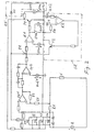
- FIG. 1 shows a basic circuit diagram of a current limiting device for carrying out the method according to the invention
- Figure 2 is a circuit diagram of a current limitation with protective circuit, evaluation device and reset device.
- a consumer V is fed from a supply voltage source Q via a series regulator LR intended for current limitation.
- the actuator F1 of the series regulator is designed as a power MOSFET in this exemplary embodiment.
- a control loop is provided consisting of a current sensor in the form of the current measuring resistor R1, a measuring amplifier MV for amplifying the current-proportional voltage drop detected at the current measuring resistor R1, a subtracting stage SUB1 for forming a difference signal between the output voltage of the measuring amplifier MV and a reference voltage Urefl and one with PID behavior trained control amplifier RV, the output of which leads to the gate of the MOSFET F1.
- the series regulator LR thus carries out a setpoint / actual value comparison and regulates the maximum current via its actuator F1.
- the gate voltage of the MOSFET F1, or the output voltage of the control amplifier RV is fed to an evaluation device in the form of the threshold value comparator K1. If the gate voltage is low, e.g. between 2 and 4 V, the MOSFET F1 operates in linear control mode to limit the current.
- the gate voltage is then less than the threshold voltage Uthr of 8 V, for example, and the threshold value comparator K1 supplies a blocking signal for a semiconductor switch F2 at its output, which is arranged parallel to the actuator F1.
- the threshold value comparator K1 supplies a switch-on signal for the semiconductor switch F2.
- the series regulator LR no longer performs a current limiting control function, but only acts as a loss-generating element between supply voltage source Q and consumer V. However, by bridging actuator F1 by switch F2, this power loss is reduced. If the same type of MOSFET is used for the semiconductor switch F2 as for the actuator F1, then the total loss-generating resistance acting only as the resistance of the parallel connection of the track resistances of the two MOSFETs.
- a greater reduction in the power loss can be achieved either by selecting a type with a lower track resistance for the MOSFET F2 or, as the exemplary embodiment according to FIG. 2 shows, connecting a plurality of similar MOSFETs F2 to F4 working in parallel with the actuator F1. All of these MOSFETs F2 to F4 can be controlled by the threshold value comparator K1.
- an operational amplifier Op1 which is coupled back via the resistors R2 and R3 can be used as the measuring amplifier MV.
- the subtracting stage SUB1 shown schematically in FIG. 1 can be implemented together with the control amplifier RV by a correspondingly connected further operational amplifier Op2.
- the reference voltage Uref1 is fed to the operational amplifier Op2 at the non-inverting input.
- the inverting input is operatively connected to the output of the operational amplifier Op1.
- the operational amplifier Op2 receives PID behavior via the RC elements in the negative feedback branch and can thus be dynamically optimally matched to the load characteristic of the consumer.
- the threshold comparator K1 is supplied with the threshold voltage Uthr at the inverting input.
- the non-inverting input is operatively connected to the output of the operational amplifier Op2.
- the output of the threshold value comparator K1 is connected via a transistor stage T1 to the gate connections of the MOSFETs F2, F3, F4. This transistor stage T1 serves to quickly discharge the high total gate capacitance of the parallel connected MOSFETS F2 to F4 in order to quickly open the MOSFETS F2 to F4 used as switches in the event of a fault.
- a protective circuit SR the output potential of the comparator K1 is evaluated via a timing element consisting of resistor R4 and capacitor C1 and a comparator K2. If the series regulator LR were to operate in current limiting mode for a longer period of time, its maximum permissible power loss would be exceeded. The time for which the series regulator LR can work in current limiting mode is specified by the timing element R4, C1. If the charging voltage at capacitor C1 reaches the voltage value of auxiliary voltage source QH2, transistor T2 is switched on Output signal of the comparator K2 controlled conductive. The potential at point P1 is forced to 0 via conductive transistor T2. Since this point P1 is connected to the gate of the MOSFET F1, the gate voltage 0 and the MOSFET F1 are switched off.
- This state of the protective circuit SR is stored via the positive feedback by the comparator K1. It is only via the reset device RS that the stored state is reset when the button S1 is closed with the two contacts S1a and S1b. At the same time, when the button S1 (switch contact S1a) is actuated, the diode D3 becomes conductive and brings the MOSFETs F1 to F4 into the blocking state. This also ensures overload protection during the reset process. The initial state is only restored after the reset has been completed. In the normal state, the resistor R4 is connected to the output of the comparator K1. In the reset state, the resistor R4 is connected to the potential of the auxiliary voltage source QH3 with 15 V, for example. The input of the comparator K2 thus carries the potential of the auxiliary voltage source QH3.
- the series regulator LR can be controlled so that only a minimum current, e.g. 10% of the nominal current.
- a minimum current e.g. 10% of the nominal current.
- transistor T2 it is advisable to use transistor T2 to switch the reference voltage Uref1 to another value.
- the arrangement according to EP 184 609 B1 which replaces the resistor R1 and the measuring amplifier MV, can advantageously be used for current detection. Using this arrangement, temperature drifts cannot falsify the current evaluation.
- the device according to the invention is particularly suitable for use in the power supply of a solar cell-powered traveling wave tube amplifier with output powers between 30 and 270 W.
Landscapes
- Engineering & Computer Science (AREA)
- Power Engineering (AREA)
- Physics & Mathematics (AREA)
- Electromagnetism (AREA)
- General Physics & Mathematics (AREA)
- Radar, Positioning & Navigation (AREA)
- Automation & Control Theory (AREA)
- Continuous-Control Power Sources That Use Transistors (AREA)
- Control Of Electrical Variables (AREA)
Claims (7)
- Procédé pour limiter le courant d'un régulateur série (LR),
caractérisé en ce que
l'organe de réglage (F1) du régulateur série (LR) est shunté de manière faiblement ohmique en mode non limitatif. - Procédé selon la revendication 1,
caractérisé en ce que
le régulateur série (LR) est coupé lorsqu'on atteint une puissance perdue autorisée, prédéterminée. - Procédé selon la revendication 1,
caractérisé en ce que
le régulateur série (LR) est commandé lorsqu'on atteint une perte de puissance autorisée, prédéterminée, pour ne plus laisser passer qu'un courant minimum. - Procédé selon l'une des revendications 1 à 3,
caractérisé en ce qu'
on exploite le fait que le régulateur série (LR) travaille en mode limitatif et, pour ce mode de fonctionnement, on génère un signal de blocage des commutateurs semiconducteurs (F2, F3, F4) qui shunte l'organe de réglage (F1) par un chemin faiblement ohmique. - Procédé selon la revendication 2,
caractérisé en ce qu'
on met en mémoire le fait d'atteindre la perte de puissance prédéterminée, et cet état mémorisé n'est terminé que par une opération de remise à l'état initial. - Procédé selon l'une des revendications 1 à 5,
caractérisé en ce que
pour shunter de manière faiblement ohmique l'organe de réglage (F1), on fait travailler en parallèle plusieurs commutateurs semi-conducteurs/moyens formant des shunts (F2, F3, F4). - Application du procédé selon l'une des revendications 1 à 6 à l'alimentation électrique par pile solaire d'un amplificateur à tube à ondes progressives.
Applications Claiming Priority (2)
| Application Number | Priority Date | Filing Date | Title |
|---|---|---|---|
| DE4128679 | 1991-08-29 | ||
| DE4128679A DE4128679C1 (fr) | 1991-08-29 | 1991-08-29 |
Publications (3)
| Publication Number | Publication Date |
|---|---|
| EP0529605A2 EP0529605A2 (fr) | 1993-03-03 |
| EP0529605A3 EP0529605A3 (en) | 1993-08-04 |
| EP0529605B1 true EP0529605B1 (fr) | 1996-11-06 |
Family
ID=6439398
Family Applications (1)
| Application Number | Title | Priority Date | Filing Date |
|---|---|---|---|
| EP92114532A Expired - Lifetime EP0529605B1 (fr) | 1991-08-29 | 1992-08-26 | Méthode pour la limitation de courant d'un régulateur serie et son application |
Country Status (2)
| Country | Link |
|---|---|
| EP (1) | EP0529605B1 (fr) |
| DE (2) | DE4128679C1 (fr) |
Families Citing this family (8)
| Publication number | Priority date | Publication date | Assignee | Title |
|---|---|---|---|---|
| DE4223339C1 (de) * | 1992-07-16 | 1994-01-20 | Ant Nachrichtentech | Überlastungsschutzschaltung |
| US5539603A (en) * | 1994-03-02 | 1996-07-23 | Maxim Integrated Products | Current protection method and apparatus and current protected low dropout voltage circuits |
| EP0674389B1 (fr) * | 1994-03-22 | 2001-10-31 | STMicroelectronics S.r.l. | Circuit de protection contre les surcharges pour circuits MOS de puissance |
| FR2720558B1 (fr) * | 1994-05-31 | 1996-06-21 | Cit Alcatel | Système d'alimentation sécurisé. |
| GB9623912D0 (en) * | 1996-11-18 | 1997-01-08 | Stc Submarine Systems Ltd | Surge protector for power feed line |
| FR2819904B1 (fr) * | 2001-01-19 | 2003-07-25 | St Microelectronics Sa | Regulateur de tension protege contre les courts-circuits |
| US7019583B2 (en) * | 2001-01-29 | 2006-03-28 | Axiohm Transaction Solutions, Inc. | Current inrush limiting circuit |
| DE102004037924A1 (de) | 2004-08-04 | 2006-03-16 | Endress + Hauser Process Solutions Ag | Modulartige Anschlußvorrichtung in einem Bussystem zum Schutz eines elektrischen Verbrauchers |
Family Cites Families (6)
| Publication number | Priority date | Publication date | Assignee | Title |
|---|---|---|---|---|
| US3723774A (en) * | 1971-08-06 | 1973-03-27 | Jerrold Electronics Corp | Power supply with temperature compensated current foldback |
| DE3535864A1 (de) * | 1985-10-08 | 1987-04-16 | Ant Nachrichtentech | Strombegrenzungsschaltung |
| FR2618276B1 (fr) * | 1987-07-15 | 1994-04-29 | Crouzet Sa | Dispositif de commutation electronique. |
| DE3728809C2 (de) * | 1987-08-28 | 1993-10-07 | Siemens Ag | Schaltungsanordnung zum Begrenzen eines Einschaltstromes |
| DE3903789C2 (de) * | 1989-02-09 | 1995-02-02 | Sel Alcatel Ag | Schaltungsanordnung zur Einschaltstrombegrenzung |
| DE4040289C1 (en) * | 1990-12-17 | 1992-02-27 | Ant Nachrichtentechnik Gmbh, 7150 Backnang, De | Current limiting circuit for slot-in contact connector - uses voltage drop across resistor to control transistor forming current source which is rapidly by=passed |
-
1991
- 1991-08-29 DE DE4128679A patent/DE4128679C1/de not_active Expired - Lifetime
-
1992
- 1992-08-26 DE DE59207483T patent/DE59207483D1/de not_active Expired - Fee Related
- 1992-08-26 EP EP92114532A patent/EP0529605B1/fr not_active Expired - Lifetime
Also Published As
| Publication number | Publication date |
|---|---|
| EP0529605A3 (en) | 1993-08-04 |
| EP0529605A2 (fr) | 1993-03-03 |
| DE59207483D1 (de) | 1996-12-12 |
| DE4128679C1 (fr) | 1992-08-27 |
Similar Documents
| Publication | Publication Date | Title |
|---|---|---|
| DE102005031622B4 (de) | Steuervorrichtung eines Halbleiterschalters | |
| DE4134537B4 (de) | Stromversorgungsschaltung für eine Entladungslampe in einem Kraftfahrzeug | |
| DE112007000411B4 (de) | Energieversorgungssteuerung | |
| EP0423885B1 (fr) | Dispositif d'alimentation avec limitation du courant d'appel | |
| DE112006001377B4 (de) | Energieversorgungssteuerung | |
| EP0666647B1 (fr) | Procédé et circuit pour commander des commutateurs semi-conducteurs montés en série | |
| EP2009764B1 (fr) | Dispositif d'alimentation en courant continue | |
| EP3414778B1 (fr) | Circuit de protection d'un module photovoltaïque (pv), procédé de fonctionnement du circuit de protection et installation photovoltaïque (pv) équipée d'un tel circuit de protection | |
| WO2007096219A1 (fr) | Ensemble circuit pourvu d'une protection contre l'alimentation en retour et servant à effectuer une commutation dans des applications de puissance | |
| EP1801973B1 (fr) | Appareil de commande | |
| EP0529605B1 (fr) | Méthode pour la limitation de courant d'un régulateur serie et son application | |
| DE102004007201A1 (de) | Überstrom-Begrenzungsschaltung | |
| WO1998043334A1 (fr) | Fusible electronique | |
| DE4039990A1 (de) | Ueberlast- und kurzschlussschutzanordnung | |
| EP0550823B1 (fr) | Procédé pour la limitation du courant au-dessus de composant de réglage et le dispositif | |
| DE102017209473A1 (de) | Verfahren zum Betreiben eines Elektro-Fahrzeugs | |
| EP0735351B1 (fr) | Montage de circuit pour détecter la température d'un élément semi-conducteur de puissance | |
| DE19546132C2 (de) | Schaltungsanordnung zum Schutz vor eingangsseitigem Überstrom bei Spannungszwischenkreisumrichtern | |
| EP0809295B1 (fr) | Mosfet avec protection en température | |
| DE4015672C2 (fr) | ||
| EP1856785B1 (fr) | Dispositif et procede pour fournir une tension continue | |
| DE10310783B4 (de) | Verfahren und Schaltungsanordnung zur Steuerung des Ausschaltvorganges eines abschaltbaren Leistungshalbleiterschalters | |
| DE102004020273B4 (de) | Steuerung eines Betriebes eines Halbleiterschalters | |
| WO1990005918A2 (fr) | Circuit de sortie universel | |
| DE10055077A1 (de) | Vorrichtung zum Verpolschutz elektrischer Komponenten |
Legal Events
| Date | Code | Title | Description |
|---|---|---|---|
| PUAI | Public reference made under article 153(3) epc to a published international application that has entered the european phase |
Free format text: ORIGINAL CODE: 0009012 |
|
| AK | Designated contracting states |
Kind code of ref document: A2 Designated state(s): BE DE FR GB IT NL |
|
| PUAL | Search report despatched |
Free format text: ORIGINAL CODE: 0009013 |
|
| AK | Designated contracting states |
Kind code of ref document: A3 Designated state(s): BE DE FR GB IT NL |
|
| 17P | Request for examination filed |
Effective date: 19930709 |
|
| 17Q | First examination report despatched |
Effective date: 19941117 |
|
| GRAG | Despatch of communication of intention to grant |
Free format text: ORIGINAL CODE: EPIDOS AGRA |
|
| GRAH | Despatch of communication of intention to grant a patent |
Free format text: ORIGINAL CODE: EPIDOS IGRA |
|
| RAP1 | Party data changed (applicant data changed or rights of an application transferred) |
Owner name: ROBERT BOSCH GMBH |
|
| GRAH | Despatch of communication of intention to grant a patent |
Free format text: ORIGINAL CODE: EPIDOS IGRA |
|
| GRAA | (expected) grant |
Free format text: ORIGINAL CODE: 0009210 |
|
| AK | Designated contracting states |
Kind code of ref document: B1 Designated state(s): BE DE FR GB IT NL |
|
| ET | Fr: translation filed | ||
| REF | Corresponds to: |
Ref document number: 59207483 Country of ref document: DE Date of ref document: 19961212 |
|
| ITF | It: translation for a ep patent filed |
Owner name: STUDIO JAUMANN |
|
| GBT | Gb: translation of ep patent filed (gb section 77(6)(a)/1977) |
Effective date: 19970123 |
|
| PLBE | No opposition filed within time limit |
Free format text: ORIGINAL CODE: 0009261 |
|
| STAA | Information on the status of an ep patent application or granted ep patent |
Free format text: STATUS: NO OPPOSITION FILED WITHIN TIME LIMIT |
|
| 26N | No opposition filed | ||
| PGFP | Annual fee paid to national office [announced via postgrant information from national office to epo] |
Ref country code: GB Payment date: 20010814 Year of fee payment: 10 |
|
| PGFP | Annual fee paid to national office [announced via postgrant information from national office to epo] |
Ref country code: NL Payment date: 20010827 Year of fee payment: 10 |
|
| PGFP | Annual fee paid to national office [announced via postgrant information from national office to epo] |
Ref country code: DE Payment date: 20011025 Year of fee payment: 10 |
|
| REG | Reference to a national code |
Ref country code: GB Ref legal event code: IF02 |
|
| PG25 | Lapsed in a contracting state [announced via postgrant information from national office to epo] |
Ref country code: GB Free format text: LAPSE BECAUSE OF NON-PAYMENT OF DUE FEES Effective date: 20020826 |
|
| PG25 | Lapsed in a contracting state [announced via postgrant information from national office to epo] |
Ref country code: DE Free format text: LAPSE BECAUSE OF NON-PAYMENT OF DUE FEES Effective date: 20030301 Ref country code: NL Free format text: LAPSE BECAUSE OF NON-PAYMENT OF DUE FEES Effective date: 20030301 |
|
| GBPC | Gb: european patent ceased through non-payment of renewal fee |
Effective date: 20020826 |
|
| NLV4 | Nl: lapsed or anulled due to non-payment of the annual fee |
Effective date: 20030301 |
|
| PGFP | Annual fee paid to national office [announced via postgrant information from national office to epo] |
Ref country code: FR Payment date: 20090819 Year of fee payment: 18 |
|
| PGFP | Annual fee paid to national office [announced via postgrant information from national office to epo] |
Ref country code: BE Payment date: 20090821 Year of fee payment: 18 |
|
| PGFP | Annual fee paid to national office [announced via postgrant information from national office to epo] |
Ref country code: IT Payment date: 20090825 Year of fee payment: 18 |
|
| BERE | Be: lapsed |
Owner name: ROBERT *BOSCH G.M.B.H. Effective date: 20100831 |
|
| REG | Reference to a national code |
Ref country code: FR Ref legal event code: ST Effective date: 20110502 |
|
| PG25 | Lapsed in a contracting state [announced via postgrant information from national office to epo] |
Ref country code: IT Free format text: LAPSE BECAUSE OF NON-PAYMENT OF DUE FEES Effective date: 20100826 |
|
| PG25 | Lapsed in a contracting state [announced via postgrant information from national office to epo] |
Ref country code: FR Free format text: LAPSE BECAUSE OF NON-PAYMENT OF DUE FEES Effective date: 20100831 Ref country code: BE Free format text: LAPSE BECAUSE OF NON-PAYMENT OF DUE FEES Effective date: 20100831 |