EP0527010A2 - Système de protection pour information critique contenue dans une mémoire - Google Patents
Système de protection pour information critique contenue dans une mémoire Download PDFInfo
- Publication number
- EP0527010A2 EP0527010A2 EP92306830A EP92306830A EP0527010A2 EP 0527010 A2 EP0527010 A2 EP 0527010A2 EP 92306830 A EP92306830 A EP 92306830A EP 92306830 A EP92306830 A EP 92306830A EP 0527010 A2 EP0527010 A2 EP 0527010A2
- Authority
- EP
- European Patent Office
- Prior art keywords
- processor
- memory
- signal
- latch
- counter
- Prior art date
- Legal status (The legal status is an assumption and is not a legal conclusion. Google has not performed a legal analysis and makes no representation as to the accuracy of the status listed.)
- Granted
Links
Images

Classifications
-
- G—PHYSICS
- G07—CHECKING-DEVICES
- G07B—TICKET-ISSUING APPARATUS; FARE-REGISTERING APPARATUS; FRANKING APPARATUS
- G07B17/00—Franking apparatus
- G07B17/00185—Details internally of apparatus in a franking system, e.g. franking machine at customer or apparatus at post office
- G07B17/00362—Calculation or computing within apparatus, e.g. calculation of postage value
- G07B2017/00395—Memory organization
- G07B2017/00403—Memory zones protected from unauthorized reading or writing
Definitions
- the invention relates generally to the protection of important or critical data in memory devices, and relates particularly to protection of such data in postage meters.
- Some single stored location must necessarily be relied upon by all parties (the customer, the postal service, and the provider of the meter) as the sole determinant of the value of the amount of postage available for printing.
- electronic postage meters that single stored location is the secure physical housing of the meter itself. Within the secure housing one or more items of data in one or more nonvolatile memories serve to determine the amount of postage available for printing.
- processors it is advantageous to guard against the possibility of a processor running amok.
- a processor is expected to execute its stored program and it is assumed the stored program contains no programming errors.
- a processor may commence executing something other than the stored program, such as data.
- the processor even though it may be executing the stored program, nonetheless behaves incorrectly due to the incorrect contents of a processor register or a memory location.
- the former may occur if, for example, the instruction pointer or program counter of the processor changes a bit due to, say, absorption of a cosmic ray.
- the latter may occur if the contents of the processor register or memory location are changed by that or other mechanisms.
- the code executed by the processor includes periodic issuance of a watchdog signal which serves to clear a watchdog circuit. If an excessive time passes without receipt of the watchdog signal, the watchdog circuit takes protective action such as shutting down the system or resetting the processor.
- the latter action has the advantage that it may restore normal processor function if, for example, the malfunction was due to a spurious change in the value of the instruction pointer or program counter.
- the watchdog circuit only triggers after the passage of a predetermined interval, and processor malfunction could conceivably alter crucial data during the predetermined interval and prior to a watchdog-induced reset. It would be most desirable if crucial data could enjoy more comprehensive safeguards against processor malfunction, with the safeguards implemented in such a way as to permit restoration of proper processor function if possible.
- a computer system typically a postage meter system, comprising a processor (CPU) having a write strobe output and address outputs and executing a stored program, a memory having a selection input and a write strobe input, and an address-decoding means for providing a selection signal to the selection input of the memory in response to associated address outputs from the processor
- the computer system including a window means comprising latch means responsive to a setting signal and a clearing signal from the processor for coupling the write strobe output of the processor with the write strobe input of the memory when the latch means is set by the setting signal, and for decoupling the write strobe output of the processor from the write strobe input of the memory when the latch means is cleared by the clearing signal, and counter means responsive to the setting signal and the clearing signal from the processor for starting a counter upon receipt of the setting signal, for clearing the counter upon receipt of the clearing signal, and for interrupting the processor in the event of the counter reaching a predetermined threshold.
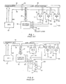
- a processor 10 is capable of writing data to memory devices 11, 12, and 13 by means of a system bus 19, of which address bus 14 and write strobe line 15 are shown.
- Some of the address lines of address bus 14 are provided to a conventional address decoder 16, these so-called “high-order” address lines are shown as the high-order portion 17 of the address bus.
- the so-called "low-order" portion 18 of the address bus 14 is provided to memory devices 11, 12, and 13, and to other devices in the memory space of processor 10.
- the data lines and other control lines of the system bus 19 are omitted from Fig. 1, as are the other devices on the system bus, such as keyboard, display, read-only memory and printer.
- the write strobe signal from the processor 10 is provided by a line 15 to the write strobe inputs 21, 22, 23 of the memory devices 11, 12, and 13 respectively.
- Memory device selection signals are provided by select lines 20 running from the address decoder 16 to "chip enable" inputs of the memory devices. For example, select lines 31, 32, and 33 provide respective select signals to corresponding chip enable inputs 41, 42, and 43 of the memory devices 11, 12, and 13, respectively.
- a line 34 from address decoder 16 is indicative generally that the address decoder selects other memory devices than those shown explicitly in Fig. 1.
- Such memory devices typically include ROM (read-only memory), and memory-mapped input/output devices such as a keyboard, a display, a printer, and discrete input/output latches.
- the write strobe signal is provided to all memory devices, including 11, 12, and 13, whenever asserted on line 15 by the processor 10. If the processor 10 were misbehaving seriously (as distinguished from the case of a processor or other system component failing in a physical, permanent way) the processor 10 could provide addresses on the address bus 14 that were meaningful to the address decoder 16, enabling one or another of memory devices 11, 12, and 13 from time to time. If the write strobe signal of line 15 were asserted during one of the periods of enablement, the contents of some or all of the memory devices 11, 12, and 13 could be lost. In the case of a postage meter, the descending register contents could be lost, a matter of great concern for both the postal patron and the postal service.
- Fig. 2 shows a known prior art system for enhancing the protection of selected memory devices, such as devices 12 and 13, here called "crucial" memory devices.
- Use of such a system might be prompted by the presence, in memory devices 12 and 13, of important postal data such as descending register data.
- memory devices 12 and 13 may be nonvolatile memories.
- memory device 11 continues to receive the write strobe signal of line 15, just as in Fig. 1, it will be noted that the crucial memory devices 12 and 13 receive a gated signal 40 at respective write strobe inputs 22 and 23.
- the selection outputs 20 of address decoder 16 are connected to respective memory devices as in Fig. 1.
- the system of Fig. 2 differs, however, in that the selection outputs 20 are also provided to multiple-input AND gate 61.
- the selection lines 32 and 33 for the crucial memory devices 12 and 13, respectively, are ORed at a gate 65 and provided directly to the AND gate 61.
- the remaining selection lines from the address decoder 16 are each inverted by inverters 67 and 69, as shown in Fig. 2, and provided to the AND gate 61.
- each possible address of the high-order address bus 17 is decoded as one or another of the selection outputs 20. If necessary, a "none-of-the-above" selection output is provided to respond to addresses having no intended physical counterpart in the system design. The result is that the number of selection outputs 20 active at any given moment is exactly one, no more and no fewer.
- the output 63 of AND gate 61 is high if (a) one of the crucial memory devices is selected and (b) none of the other memory devices is selected.
- Signal 63 is one of two inputs toAND gate 62; the other is the write strobe signal of line 15.
- the crucial memory devices then, receive write strobe signals only when one or another of the crucial memory devices is currently being selected by the address decoder 16.
- the system of Fig. 2 offers no protection of crucial data beyond that of Fig. 1.
- the gates 61 and 62 have no effect.
- the gates 61 and 62 only serve to block write strobe inputs at 22 and 23 which would in any event be ignored by memory devices 12 and 13 because of the lack of asserted selection signals on lines 32 and 33.
- a processor 10 misbehaving seriously in a system of Fig. 2 that is electrically sound will be capable of destroying data in the crucial memory devices simply by presenting their addresses on the address bus 14.
- the processor 10 When the processor 10 presents a valid address on the address bus 14, the corresponding selection line, for example line 32, will be asserted and will be received at the chip-enable input 42 of memory device 12. Likewise, the a strobe signal on line 40 will be made available to the write strobe input 22 of memory device 12. The possible result is loss or damage to the contents of memory device 12.
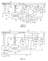
- Fig. 3 shows another prior-art system intended to protect data in crucial memory devices, say memory devices 12 and 13.
- the processor 10, address bus 14 and 17, and address decoder 16 are as in Fig. 1.
- Memory device 11, which is not a crucial memory device, receives the write strobe signal of line 15 directly, as in Fig. 1, and receives its corresponding selection signal 31 directly, also as in Fig. 1.
- Crucial memory devices 12 and 13 do not receive selection signals or the write strobe signal directly. Instead, AND gates 51, 52, and 53 are provided, blocking the selection signals 32 and 33 and the write strobe signal of line 15 under circumstances which will presently be described.
- the selection outputs for the crucial memory devices are provided to a NOR gate 54.
- the processor 10 is not attempting access to the crucial memory devices 12 and 13, and so select signals 32 and 33 remain unasserted (here assumed to be a low logic level); as a result the output 55 of gate 54 is high. This clears counter 56.
- an address line 32 or 33 may continue to be asserted for some lengthy period of time.
- a mechanical defect in the address bus 14 and 17, in the address decoder 16, or in the wiring of lines 31, 32, 33, and 34 may give rise to continued selection of a crucial memory device 12 or 13.
- a consequence of such a mechanical defect could be a write instruction from the processor 10 that is intended for, say, memory device 11, but which, due to the mechanical malfunction, would cause a change in the contents of memory devices 12 or 13 as well.
- the system of Fig. 3 offers protection against certain mechanical failures, it provides only limited protection against the prospect of a processor misbehaving seriously. As will now be described, the system of Fig. 3 will fail to detect many of the possible ways a processor may misbehave, and will be successful at protecting against only a particular subset of the possible ways of misbehavior.
- memory read and memory write instructions carried out on the system bus represent only a portion of all the bus activities.
- the processor Prior to the processor's execution of an instruction forming part of the stored program, the processor must necessarily have fetched the instruction from a memory device on the system bus.
- the fetch activity is electrically very similar to a memory read activity, and each includes a step of the processor 10 providing an address on the system bus.
- the address decoder 16 handles memory read addresses the same way it handles fetch addresses. In a system functioning properly it is expected that the fetch addresses will represent retrieval of data (i.e. instructions for execution) only from locations that contain data, namely from the memory devices containing the stored program.
- processor 10 Under the normal steps of a typical stored program (in a system having no mechanical defects) it is expected that processor 10, shortly after initiating bus access to an address giving rise to the assertion of selection lines 32 or 33, will proceed to bus access elsewhere in the address space of the processor. Such bus access elsewhere would reset the counter 56 and avert the decoupling of gates 51, 52, and 53.
- the conventional fetching of instructions for execution may cause the address decoder to stop asserting selection lines 32 and 33 and to assert instead the selection line for some memory device containing stored program. This would be the usual process in a system lacking any mechanical defect. Thus, fetching (at least in a system that is free of mechanical defect) would generally keep the counter 56 reset more or less continuously, except in the special case of processor malfunction where the instruction pointer or program counter happened to point to a crucial memory.
- FIG. 4 a block diagram shows a system of an embodiment of the invention.
- Processor 10 provides address signals to the address bus 14 and to the address decoder 16, just as in the system of Fig. 1.
- the memory devices 11, 12, 13 all receive respective selection signals from the address decoder 16 just as in the system of Fig. 1.
- Memory device 11 receives the write strobe signal of line 15 as in the system of Fig. 1.
- Crucial memory devices 12 and 13, however, receive inputs at their write strobe inputs 22 and 23 not from line 15 but from a window circuit 70.
- Window circuit 70 receives requests from the processor 10 by I/O port transactions or, preferably, by memory-mapped I/o transactions. In the latter arrangement a selection signal 35 from address decoder 16 is provided to the window circuit 70, and preferably it also receives low-order address bits from low-order address bus 18.
- an output 86 of latch 80 is normally low.
- the normally-low state of line 86 turns off an AND gate 81 so that a write strobe signal 72 for the memory 12 is unasserted.
- the write strobe signal of line 15 does not have any effect on the output 72 of the window circuit 70.
- an output 73 is also unasserted.
- the processor 10 gains write access to crucial memory devices 12 or 13 as follows. Referring now to Fig. 5, to write to memory device 12 the processor writes a command to the latch 80 representative of a request for access.
- the output 86 of latch 80 goes high, turning on the gate 81 and permitting write strobe signals of the line 15 to be communicated to the output 72 of the window circuit, and thence to the write strobe input of memory device 12.
- the high level of line 86 causes an inverter 82 to go low, removing the clear input to the counter 83.
- Counter 83 commences counting, and if it reaches a preset threshold its output 87 goes high, turning on OR gate 85. This resets the processor 10.
- the preset threshold of counter 83 is changeable by commands to a latch 84 from the processor.
- the processor 10 would write a second command to latch 80 shortly after making its accesses to memory device 12, causing the output 86 of latch 80 to return to its normal, low state. This would reset the counter 83 and avert any resetting of the processor 10.
- a setting signal a command (called a setting signal) to a latch 90 to turn on the line 96
- the clock 93 will begin counting.
- the processor 10 would fairly promptly write a second command (called a clearing signal) to latch 90, cutting off the write strobe signal to device 13 and clearing the counter 93.
- the counter 93 is programmable by commands to a latch 94.
- each of the counters is individually programmable. This is desired because the memories 12, 13 are preferably of different storage technologies, for which different writing and access times may apply. Thus a memory of a technology with a slow access time may be accommodated by programming its respective counter for a longer interval, while memory of a technology with a fast access time may be more closely protected by programming its respective counter for a shorter interval.
- the gate 81 is initially enabled by a flip-flop (not shown in Fig. 5) upon power-on, and continues to be enabled regardless of the state of latch 80.
- the additional logic is arranged so that a subsequent signal from the processor sets the flip-flop so that it no longer enables gate 81. From that point onwards the gate 81 is enabled only by the latch 80.
- the first memory is an EEPROM (electrically erasible programmable read only read only memory) and the second memory is a battery-backed-up CMOS RAM (complementary metal-oxide semiconductor random access memory).
- the first predetermined threshold is about 341 milliseconds, and the second predetermined threshold is about 682 milliseconds, all selected for an eight-bit processor running at 6 MHz.
- the reset signal 71 may be seen which, if asserted, causes a reset to the processor 10 at its reset input 75.
- this could be any hardware interrupt to the processor 10, but preferably it is the reset input, which may be thought of as the highest priority hardware interrupt.
- the reset input causes program execution from the instruction at memory location zero, thus eliminating any possible problem with spurious contents of the instruction pointer or program counter.
- the reset input also resets all other internal states of the processor 10, thus eliminating any possible problem with spurious internal states of the processor 10. Where the condition giving rise to one or another of the counters 83, 93 reaching its threshold was a processor misbehaving seriously, then, there is the possibility the processor will execute its stored program correctly thereafter.
- a latch 74 is provided, external to the processor 10 and capable of latching the reset signal 71.
- the stored program for processor 10 preferably has steps that check, upon execution starting at zero, to see whether the latch 74 is set. If it is not, the assumption is that the execution from zero was due to initial application of power. If latch 74 is set, the assumption is that execution from zero was due to a reset from the window circuit 70, and the processor can appropriately note the event. Repeated notations of a reset due to the window circuit 70 will preferably cause the processor 10, under stored program control, to annunciate an appropriate warning message to the user.
- the counter 83 or (93) starts counting with the event of the processor 10 sending the command to the latch 80 (or 90) for access to the memory device. This gives the counter a head start in detecting problems, as compared with the counter 56 of Fig. 3, which only starts counting with the occurrence of a selection signal from the address decoder 16.
- the counter 83 or (93) runs freely until such time as a command for ceasing access to the memory device is received at the latch 80 (or 90).
- the counter 56 will be cleared every time the processor 10 happens to make reference, by memory reading and writing or by instruction fetching, to any address outside the crucial memories 12,13.
- the protective action taken by the system of Fig. 3 is no more than interrupting the connection of write strobe and/or selection lines.
- the system of Figs. 4 and 5 takes the step of interrupting (and preferably resetting) the processor, which will at least sometimes remedy completely the condition giving rise to the malfunction.
Applications Claiming Priority (2)
| Application Number | Priority Date | Filing Date | Title |
|---|---|---|---|
| US07/740,427 US5276844A (en) | 1991-08-05 | 1991-08-05 | Protection system for critical memory information |
| US740427 | 2000-12-19 |
Publications (3)
| Publication Number | Publication Date |
|---|---|
| EP0527010A2 true EP0527010A2 (fr) | 1993-02-10 |
| EP0527010A3 EP0527010A3 (en) | 1993-11-18 |
| EP0527010B1 EP0527010B1 (fr) | 1996-04-24 |
Family
ID=24976459
Family Applications (1)
| Application Number | Title | Priority Date | Filing Date |
|---|---|---|---|
| EP92306830A Expired - Lifetime EP0527010B1 (fr) | 1991-08-05 | 1992-07-27 | Système de protection pour information critique contenue dans une mémoire |
Country Status (8)
| Country | Link |
|---|---|
| US (1) | US5276844A (fr) |
| EP (1) | EP0527010B1 (fr) |
| JP (1) | JPH05225067A (fr) |
| AT (1) | ATE137348T1 (fr) |
| CA (1) | CA2072504A1 (fr) |
| DE (1) | DE69210135T2 (fr) |
| DK (1) | DK0527010T3 (fr) |
| SG (1) | SG49193A1 (fr) |
Cited By (6)
| Publication number | Priority date | Publication date | Assignee | Title |
|---|---|---|---|---|
| EP0657823A2 (fr) * | 1993-12-09 | 1995-06-14 | Pitney Bowes Inc. | Circuit de protection d'accès en mémoire avec une clé de chiffrement |
| EP0657821A2 (fr) * | 1993-12-09 | 1995-06-14 | Pitney Bowes Inc. | Circuit de surveillance de mémoire pour la détection de l'accès non autorisé à la mémoire |
| EP0657822A1 (fr) * | 1993-12-09 | 1995-06-14 | Pitney Bowes Inc. | Circuit pour limiter l'accès multiple pour un dispositf de mémoire multiple |
| EP0658847A1 (fr) * | 1993-12-09 | 1995-06-21 | Pitney Bowes Inc. | Décodeur d'adresse avec allocation de mémoire et détection d'adresse illégal pour un système de micro-contrôleur |
| EP0608060B1 (fr) * | 1993-01-11 | 2000-03-08 | Ascom Autelca Ltd. | Méthode et dispositif de protection de données |
| US7257558B2 (en) | 1996-04-23 | 2007-08-14 | Neopost Technologies | System and method for conducting a financial transaction between a sender and recipient of a mail piece |
Families Citing this family (13)
| Publication number | Priority date | Publication date | Assignee | Title |
|---|---|---|---|---|
| JP2697621B2 (ja) * | 1994-07-29 | 1998-01-14 | 日本電気株式会社 | 信号周期検出回路および信号断監視回路 |
| US6176178B1 (en) | 1995-03-07 | 2001-01-23 | Ascom Hasler Mailing Systems Ag | Tamper-resistant postage meter |
| US5706727A (en) * | 1995-03-14 | 1998-01-13 | Ascom Hasler Mailing Systems Ag | Postage meter with improved paper path |
| US5668973A (en) * | 1995-04-14 | 1997-09-16 | Ascom Hasler Mailing Systems Ag | Protection system for critical memory information |
| US5719381A (en) * | 1995-04-14 | 1998-02-17 | Ascom Hasler Mailing Systems Ag | Postage meter with hollow rotor axle |
| US5654614A (en) * | 1995-04-14 | 1997-08-05 | Ascom Hasler Mailing Systems Ag | Single-motor setting and printing postage meter |
| US5746133A (en) * | 1995-05-22 | 1998-05-05 | Ascom Hasler Mailing Systems Ag | Postage meter with rotor movement and die cover sensor |
| US5689098A (en) * | 1995-05-26 | 1997-11-18 | Ascom Hasler Mailing Systems Ag | Postage meter with improved postal lock |
| KR0146551B1 (ko) * | 1995-08-21 | 1998-09-15 | 양승택 | 임계영역을 지원하는 래치 관리방법 |
| US6842742B1 (en) | 1996-04-23 | 2005-01-11 | Ascom Hasler Mailing Systems, Inc. | System for providing early warning preemptive postal equipment replacement |
| EP0840919B1 (fr) * | 1996-04-23 | 2004-10-06 | Ascom Hasler Mailing Systems, Inc. | Systeme visant a effectuer un remplacement preventif d'une machine a affranchir |
| DE202006002263U1 (de) * | 2006-02-14 | 2006-04-20 | Abb Patent Gmbh | Druckmessumformer |
| US10957445B2 (en) | 2017-10-05 | 2021-03-23 | Hill-Rom Services, Inc. | Caregiver and staff information system |
Citations (5)
| Publication number | Priority date | Publication date | Assignee | Title |
|---|---|---|---|---|
| US4332009A (en) * | 1980-01-21 | 1982-05-25 | Mostek Corporation | Memory protection system |
| EP0109504A2 (fr) * | 1982-11-18 | 1984-05-30 | International Business Machines Corporation | Système de protection pour dispositifs de mémoire, d'entrée-sortie et équivalents |
| EP0223130A2 (fr) * | 1985-10-31 | 1987-05-27 | Alcatel Satmam | Circuit pour machine d'affranchissement électronique |
| EP0356052A2 (fr) * | 1988-08-18 | 1990-02-28 | Neopost Limited | Machine à affranchir |
| EP0376486A2 (fr) * | 1988-12-30 | 1990-07-04 | Pitney Bowes, Inc. | Machine à affranchir électronique ayant une modification dans l'organisation d'une mémoire non volatile |
Family Cites Families (22)
| Publication number | Priority date | Publication date | Assignee | Title |
|---|---|---|---|---|
| US4376299A (en) * | 1980-07-14 | 1983-03-08 | Pitney Bowes, Inc. | Data center for remote postage meter recharging system having physically secure encrypting apparatus and employing encrypted seed number signals |
| US4566106A (en) * | 1982-01-29 | 1986-01-21 | Pitney Bowes Inc. | Electronic postage meter having redundant memory |
| US4644494A (en) * | 1984-02-06 | 1987-02-17 | Sundstrand Data Control, Inc. | Solid state memory for aircraft flight data recorder systems |
| US4618953A (en) * | 1984-05-01 | 1986-10-21 | Pitney Bowes Inc. | Watchdog circuit |
| DE3421540A1 (de) * | 1984-06-08 | 1986-01-02 | Audi AG, 8070 Ingolstadt | Schliesssystem mit einem batteriebetriebenen infrarot-handsender |
| JPS6162161A (ja) * | 1984-08-22 | 1986-03-31 | ピツトネイ・ボウズ・インコーポレーテツド | 電子郵便料金計用リアルタイム及びパワーダウンデータ記憶能力を有する不揮発メモリ |
| US4706215A (en) * | 1984-08-22 | 1987-11-10 | Pitney Bowes Inc. | Data protection system for electronic postage meters having multiple non-volatile multiple memories |
| US4639918A (en) * | 1985-01-18 | 1987-01-27 | Pitney Bowes Inc. | Diagnostic control keyboard for a mailing machine |
| US4644541A (en) * | 1985-01-18 | 1987-02-17 | Pitney Bowes Inc. | Diagnostic test for programmable device in a mailing machine |
| US4998203A (en) * | 1985-03-12 | 1991-03-05 | Digiulio Peter C | Postage meter with a non-volatile memory security circuit |
| US4698829A (en) * | 1985-03-12 | 1987-10-06 | Pitney Bowes Inc. | Monitoring system for verifying that an input signal is toggling at a minimum frequency |
| US4746818A (en) * | 1985-03-12 | 1988-05-24 | Pitney Bowes Inc. | Circuit for maintaining the state of an output despite changes in the state of input |
| US4710882A (en) * | 1985-03-12 | 1987-12-01 | Pitney Bowes Inc. | Electronic postage meter having a nonvolatile memory selection means |
| FR2584557B1 (fr) * | 1985-07-02 | 1989-07-28 | Smh Alcatel | Systeme de telecontrole pour machines a affranchir |
| US4805109A (en) * | 1985-10-16 | 1989-02-14 | Pitney Bowes Inc. | Nonvolatile memory protection arrangement for electronic postage meter system having plural nonvolatile memories |
| US4845632A (en) * | 1985-10-16 | 1989-07-04 | Pitney Bowes Inc. | Electonic postage meter system having arrangement for rapid storage of critical postage accounting data in plural nonvolatile memories |
| US4802117A (en) * | 1985-12-16 | 1989-01-31 | Pitney Bowes Inc. | Method of preserving data storage in a postal meter |
| US4962459A (en) * | 1985-12-26 | 1990-10-09 | Mallozzi Joseph D | System for accounting for postage expended by a postage meter having data security during printing |
| US4837702A (en) * | 1986-04-28 | 1989-06-06 | Pitney Bowes Inc. | Electronic postage meter having an infinite loop lockout arrangement |
| US4843572A (en) * | 1987-05-14 | 1989-06-27 | Pitney Bowes Inc. | Inking control method and apparatus for a mailing machine |
| WO1989011134A1 (fr) * | 1988-05-09 | 1989-11-16 | Ascom Hasler Ag | Systeme electronique de calcul et d'enregistrement pour machines d'affranchissement |
| US5193165A (en) * | 1989-12-13 | 1993-03-09 | International Business Machines Corporation | Memory card refresh buffer |
-
1991
- 1991-08-05 US US07/740,427 patent/US5276844A/en not_active Expired - Fee Related
-
1992
- 1992-06-26 CA CA002072504A patent/CA2072504A1/fr not_active Abandoned
- 1992-07-27 DE DE69210135T patent/DE69210135T2/de not_active Expired - Fee Related
- 1992-07-27 EP EP92306830A patent/EP0527010B1/fr not_active Expired - Lifetime
- 1992-07-27 DK DK92306830.8T patent/DK0527010T3/da active
- 1992-07-27 SG SG1996007456A patent/SG49193A1/en unknown
- 1992-07-27 AT AT92306830T patent/ATE137348T1/de not_active IP Right Cessation
- 1992-07-29 JP JP4202472A patent/JPH05225067A/ja active Pending
Patent Citations (5)
| Publication number | Priority date | Publication date | Assignee | Title |
|---|---|---|---|---|
| US4332009A (en) * | 1980-01-21 | 1982-05-25 | Mostek Corporation | Memory protection system |
| EP0109504A2 (fr) * | 1982-11-18 | 1984-05-30 | International Business Machines Corporation | Système de protection pour dispositifs de mémoire, d'entrée-sortie et équivalents |
| EP0223130A2 (fr) * | 1985-10-31 | 1987-05-27 | Alcatel Satmam | Circuit pour machine d'affranchissement électronique |
| EP0356052A2 (fr) * | 1988-08-18 | 1990-02-28 | Neopost Limited | Machine à affranchir |
| EP0376486A2 (fr) * | 1988-12-30 | 1990-07-04 | Pitney Bowes, Inc. | Machine à affranchir électronique ayant une modification dans l'organisation d'une mémoire non volatile |
Cited By (11)
| Publication number | Priority date | Publication date | Assignee | Title |
|---|---|---|---|---|
| EP0608060B1 (fr) * | 1993-01-11 | 2000-03-08 | Ascom Autelca Ltd. | Méthode et dispositif de protection de données |
| EP0657823A2 (fr) * | 1993-12-09 | 1995-06-14 | Pitney Bowes Inc. | Circuit de protection d'accès en mémoire avec une clé de chiffrement |
| EP0657821A2 (fr) * | 1993-12-09 | 1995-06-14 | Pitney Bowes Inc. | Circuit de surveillance de mémoire pour la détection de l'accès non autorisé à la mémoire |
| EP0657822A1 (fr) * | 1993-12-09 | 1995-06-14 | Pitney Bowes Inc. | Circuit pour limiter l'accès multiple pour un dispositf de mémoire multiple |
| EP0658847A1 (fr) * | 1993-12-09 | 1995-06-21 | Pitney Bowes Inc. | Décodeur d'adresse avec allocation de mémoire et détection d'adresse illégal pour un système de micro-contrôleur |
| EP0657821A3 (fr) * | 1993-12-09 | 1996-04-17 | Pitney Bowes Inc | Circuit de surveillance de mémoire pour la détection de l'accès non autorisé à la mémoire. |
| EP0657823A3 (fr) * | 1993-12-09 | 1996-04-17 | Pitney Bowes Inc | Circuit de protection d'accès en mémoire avec une clé de chiffrement. |
| US5729716A (en) * | 1993-12-09 | 1998-03-17 | Pitney Bowes Inc. | Memory monitoring circuit for detecting unauthorized memory access |
| US5732245A (en) * | 1993-12-09 | 1998-03-24 | Pitney Bowes Inc. | Multi-memory access limiting circuit for a multi-memory device |
| US7257558B2 (en) | 1996-04-23 | 2007-08-14 | Neopost Technologies | System and method for conducting a financial transaction between a sender and recipient of a mail piece |
| US7769694B2 (en) | 1996-04-23 | 2010-08-03 | Neopost Technologies | Secure postage payment system and method |
Also Published As
| Publication number | Publication date |
|---|---|
| JPH05225067A (ja) | 1993-09-03 |
| DE69210135D1 (de) | 1996-05-30 |
| SG49193A1 (en) | 1998-05-18 |
| EP0527010B1 (fr) | 1996-04-24 |
| CA2072504A1 (fr) | 1993-02-06 |
| ATE137348T1 (de) | 1996-05-15 |
| DK0527010T3 (da) | 1996-08-26 |
| US5276844A (en) | 1994-01-04 |
| EP0527010A3 (en) | 1993-11-18 |
| DE69210135T2 (de) | 1996-11-28 |
Similar Documents
| Publication | Publication Date | Title |
|---|---|---|
| EP0608060B1 (fr) | Méthode et dispositif de protection de données | |
| EP0527010B1 (fr) | Système de protection pour information critique contenue dans une mémoire | |
| US5668973A (en) | Protection system for critical memory information | |
| US4685056A (en) | Computer security device | |
| US4959860A (en) | Power-on password functions for computer system | |
| US6453417B1 (en) | Microcontroller with secure signature extraction | |
| CA1153474A (fr) | Circuit de protection contre les mises en memoire accidentelles | |
| KR101110994B1 (ko) | 에러 동작으로부터 집적 회로를 보호하는 방법 및 장치 | |
| US5396609A (en) | Method of protecting programs and data in a computer against unauthorized access and modification by monitoring address regions | |
| JP5535547B2 (ja) | セキュアメモリインターフェース | |
| US5576650A (en) | Reset circuit of electronic device | |
| US5040178A (en) | Method of fault protection for a microcomputer system | |
| EP2257860B1 (fr) | Procédé et appareil de protection contre une réinitialisation matérielle | |
| KR100736963B1 (ko) | 에러에 중립적인 명령을 추적하여 마이크로프로세서에서의폴스 에러 검출을 줄이는 장치 및 방법 | |
| CA2072494A1 (fr) | Boucle anti-mise hors circuit en cas de panne d'alimentation momentanee | |
| US4742469A (en) | Electronic meter circuitry | |
| US20120233499A1 (en) | Device for Improving the Fault Tolerance of a Processor | |
| US20040078735A1 (en) | Flexible method for satisfying complex system error handling requirements via error promotion/demotion | |
| US10452844B2 (en) | Protecting isolated secret data of integrated circuit devices | |
| JP2857708B2 (ja) | 信頼性あるウォッチドッグタイマ | |
| US8230286B1 (en) | Processor reliability improvement using automatic hardware disablement | |
| JP3253296B2 (ja) | 記憶装置及びデータ処理装置 | |
| JP3204384B2 (ja) | 半導体記憶回路 | |
| JP2870083B2 (ja) | ウオッチドッグタイマ内蔵マイクロコンピュータ | |
| JPH11306047A (ja) | 暴走検出装置 |
Legal Events
| Date | Code | Title | Description |
|---|---|---|---|
| PUAI | Public reference made under article 153(3) epc to a published international application that has entered the european phase |
Free format text: ORIGINAL CODE: 0009012 |
|
| AK | Designated contracting states |
Kind code of ref document: A2 Designated state(s): AT BE CH DE DK ES FR GB IT LI NL PT SE |
|
| PUAL | Search report despatched |
Free format text: ORIGINAL CODE: 0009013 |
|
| AK | Designated contracting states |
Kind code of ref document: A3 Designated state(s): AT BE CH DE DK ES FR GB IT LI NL PT SE |
|
| 17P | Request for examination filed |
Effective date: 19940518 |
|
| RAP1 | Party data changed (applicant data changed or rights of an application transferred) |
Owner name: ASCOM HASLER MAILING SYSTEMS AG |
|
| 17Q | First examination report despatched |
Effective date: 19950602 |
|
| GRAH | Despatch of communication of intention to grant a patent |
Free format text: ORIGINAL CODE: EPIDOS IGRA |
|
| GRAA | (expected) grant |
Free format text: ORIGINAL CODE: 0009210 |
|
| AK | Designated contracting states |
Kind code of ref document: B1 Designated state(s): AT BE CH DE DK ES FR GB IT LI NL PT SE |
|
| PG25 | Lapsed in a contracting state [announced via postgrant information from national office to epo] |
Ref country code: ES Free format text: THE PATENT HAS BEEN ANNULLED BY A DECISION OF A NATIONAL AUTHORITY Effective date: 19960424 Ref country code: AT Effective date: 19960424 |
|
| REF | Corresponds to: |
Ref document number: 137348 Country of ref document: AT Date of ref document: 19960515 Kind code of ref document: T |
|
| ITF | It: translation for a ep patent filed |
Owner name: BARZANO' E ZANARDO ROMA S.P.A. |
|
| REG | Reference to a national code |
Ref country code: CH Ref legal event code: NV Representative=s name: KIRKER & CIE SA |
|
| REF | Corresponds to: |
Ref document number: 69210135 Country of ref document: DE Date of ref document: 19960530 |
|
| ET | Fr: translation filed | ||
| PG25 | Lapsed in a contracting state [announced via postgrant information from national office to epo] |
Ref country code: PT Effective date: 19960724 |
|
| REG | Reference to a national code |
Ref country code: DK Ref legal event code: T3 |
|
| PLBE | No opposition filed within time limit |
Free format text: ORIGINAL CODE: 0009261 |
|
| STAA | Information on the status of an ep patent application or granted ep patent |
Free format text: STATUS: NO OPPOSITION FILED WITHIN TIME LIMIT |
|
| 26N | No opposition filed | ||
| REG | Reference to a national code |
Ref country code: GB Ref legal event code: IF02 |
|
| PGFP | Annual fee paid to national office [announced via postgrant information from national office to epo] |
Ref country code: DK Payment date: 20020611 Year of fee payment: 11 |
|
| PGFP | Annual fee paid to national office [announced via postgrant information from national office to epo] |
Ref country code: SE Payment date: 20020617 Year of fee payment: 11 Ref country code: CH Payment date: 20020617 Year of fee payment: 11 |
|
| PGFP | Annual fee paid to national office [announced via postgrant information from national office to epo] |
Ref country code: NL Payment date: 20020619 Year of fee payment: 11 |
|
| PGFP | Annual fee paid to national office [announced via postgrant information from national office to epo] |
Ref country code: BE Payment date: 20020724 Year of fee payment: 11 |
|
| PG25 | Lapsed in a contracting state [announced via postgrant information from national office to epo] |
Ref country code: SE Free format text: LAPSE BECAUSE OF NON-PAYMENT OF DUE FEES Effective date: 20030728 |
|
| PG25 | Lapsed in a contracting state [announced via postgrant information from national office to epo] |
Ref country code: LI Free format text: LAPSE BECAUSE OF NON-PAYMENT OF DUE FEES Effective date: 20030731 Ref country code: DK Free format text: LAPSE BECAUSE OF NON-PAYMENT OF DUE FEES Effective date: 20030731 Ref country code: CH Free format text: LAPSE BECAUSE OF NON-PAYMENT OF DUE FEES Effective date: 20030731 Ref country code: BE Free format text: LAPSE BECAUSE OF NON-PAYMENT OF DUE FEES Effective date: 20030731 |
|
| BERE | Be: lapsed |
Owner name: *ASCOM HASLER MAILING SYSTEMS A.G. Effective date: 20030731 |
|
| PG25 | Lapsed in a contracting state [announced via postgrant information from national office to epo] |
Ref country code: NL Free format text: LAPSE BECAUSE OF NON-PAYMENT OF DUE FEES Effective date: 20040201 |
|
| EUG | Se: european patent has lapsed | ||
| REG | Reference to a national code |
Ref country code: CH Ref legal event code: PL Ref country code: DK Ref legal event code: EBP |
|
| NLV4 | Nl: lapsed or anulled due to non-payment of the annual fee |
Effective date: 20040201 |
|
| PGFP | Annual fee paid to national office [announced via postgrant information from national office to epo] |
Ref country code: IT Payment date: 20070726 Year of fee payment: 16 |
|
| PGFP | Annual fee paid to national office [announced via postgrant information from national office to epo] |
Ref country code: DE Payment date: 20080722 Year of fee payment: 17 |
|
| PGFP | Annual fee paid to national office [announced via postgrant information from national office to epo] |
Ref country code: FR Payment date: 20080715 Year of fee payment: 17 |
|
| PGFP | Annual fee paid to national office [announced via postgrant information from national office to epo] |
Ref country code: GB Payment date: 20080722 Year of fee payment: 17 |
|
| PG25 | Lapsed in a contracting state [announced via postgrant information from national office to epo] |
Ref country code: IT Free format text: LAPSE BECAUSE OF NON-PAYMENT OF DUE FEES Effective date: 20080727 |
|
| GBPC | Gb: european patent ceased through non-payment of renewal fee |
Effective date: 20090727 |
|
| REG | Reference to a national code |
Ref country code: FR Ref legal event code: ST Effective date: 20100331 |
|
| PG25 | Lapsed in a contracting state [announced via postgrant information from national office to epo] |
Ref country code: FR Free format text: LAPSE BECAUSE OF NON-PAYMENT OF DUE FEES Effective date: 20090731 |
|
| PG25 | Lapsed in a contracting state [announced via postgrant information from national office to epo] |
Ref country code: GB Free format text: LAPSE BECAUSE OF NON-PAYMENT OF DUE FEES Effective date: 20090727 |
|
| PG25 | Lapsed in a contracting state [announced via postgrant information from national office to epo] |
Ref country code: DE Free format text: LAPSE BECAUSE OF NON-PAYMENT OF DUE FEES Effective date: 20100202 |