EP0523885A1 - Détecteur de phase pour circuits de récupération d'informations et de l'horloge à haute fréquence - Google Patents
Détecteur de phase pour circuits de récupération d'informations et de l'horloge à haute fréquence Download PDFInfo
- Publication number
- EP0523885A1 EP0523885A1 EP92306098A EP92306098A EP0523885A1 EP 0523885 A1 EP0523885 A1 EP 0523885A1 EP 92306098 A EP92306098 A EP 92306098A EP 92306098 A EP92306098 A EP 92306098A EP 0523885 A1 EP0523885 A1 EP 0523885A1
- Authority
- EP
- European Patent Office
- Prior art keywords
- signal
- pulse
- data
- phase error
- clock signal
- Prior art date
- Legal status (The legal status is an assumption and is not a legal conclusion. Google has not performed a legal analysis and makes no representation as to the accuracy of the status listed.)
- Withdrawn
Links
Images


Classifications
-
- H—ELECTRICITY
- H03—ELECTRONIC CIRCUITRY
- H03L—AUTOMATIC CONTROL, STARTING, SYNCHRONISATION, OR STABILISATION OF GENERATORS OF ELECTRONIC OSCILLATIONS OR PULSES
- H03L7/00—Automatic control of frequency or phase; Synchronisation
- H03L7/06—Automatic control of frequency or phase; Synchronisation using a reference signal applied to a frequency- or phase-locked loop
- H03L7/08—Details of the phase-locked loop
- H03L7/085—Details of the phase-locked loop concerning mainly the frequency- or phase-detection arrangement including the filtering or amplification of its output signal
-
- H—ELECTRICITY
- H03—ELECTRONIC CIRCUITRY
- H03L—AUTOMATIC CONTROL, STARTING, SYNCHRONISATION, OR STABILISATION OF GENERATORS OF ELECTRONIC OSCILLATIONS OR PULSES
- H03L7/00—Automatic control of frequency or phase; Synchronisation
- H03L7/06—Automatic control of frequency or phase; Synchronisation using a reference signal applied to a frequency- or phase-locked loop
- H03L7/08—Details of the phase-locked loop
- H03L7/099—Details of the phase-locked loop concerning mainly the controlled oscillator of the loop
- H03L7/0991—Details of the phase-locked loop concerning mainly the controlled oscillator of the loop the oscillator being a digital oscillator, e.g. composed of a fixed oscillator followed by a variable frequency divider
-
- H—ELECTRICITY
- H04—ELECTRIC COMMUNICATION TECHNIQUE
- H04L—TRANSMISSION OF DIGITAL INFORMATION, e.g. TELEGRAPHIC COMMUNICATION
- H04L7/00—Arrangements for synchronising receiver with transmitter
- H04L7/0016—Arrangements for synchronising receiver with transmitter correction of synchronization errors
- H04L7/002—Arrangements for synchronising receiver with transmitter correction of synchronization errors correction by interpolation
- H04L7/0025—Arrangements for synchronising receiver with transmitter correction of synchronization errors correction by interpolation interpolation of clock signal
-
- H—ELECTRICITY
- H04—ELECTRIC COMMUNICATION TECHNIQUE
- H04L—TRANSMISSION OF DIGITAL INFORMATION, e.g. TELEGRAPHIC COMMUNICATION
- H04L7/00—Arrangements for synchronising receiver with transmitter
- H04L7/02—Speed or phase control by the received code signals, the signals containing no special synchronisation information
- H04L7/033—Speed or phase control by the received code signals, the signals containing no special synchronisation information using the transitions of the received signal to control the phase of the synchronising-signal-generating means, e.g. using a phase-locked loop
Definitions
- the present invention relates generally to phase detectors used in very high frequency (e.g., greater than 50 MHz) phase-locked loops, and particularly to phase detectors used in clock and data recovery circuits for NRZ (non-return to zero) and NRZI (non-return to zero inverted) data streams.
- phase-locked loop PLL
- recovered clock An essential function of a clock and data recovery circuit is the recovery of the clock signal from the incoming data transitions such that the recovered clock is able to sample the incoming data at the optimum positions (centers) of the data symbols.
- NRZ non-return to zero
- NRZI non-return to zero inverted
- bit frames are overlaid on an oscilloscope screen, a pattern known as the "eye opening" is formed.
- the signal value must be sampled in order to decode the bit value for that frame. While sampling in the center of each bit frame is the ideal, circuit delays and other signal distortions may make it extremely difficult for the PLL to precisely track the bit frame center.
- phase detectors used in NRZ data recovery circuits are typically used in NRZ data recovery circuits.
- phase detectors e.g., multiplier or exclusive-OR phase detectors
- a non-linear element such as a squaring device
- data signals in the data recovery signal path must be delayed by the same amount of time as the signals which go through the non-linear element used for clock recovery.
- the present invention overcomes the delay mismatch problem by eliminating the need for separate signal paths for data recovery and clock recovery, as well as using identical circuits, with virtually identical delay, for both data and clock signals.
- DCD duty-cycle distortion
- DDJ data pattern dependent jitters
- phase detector In order to accurately decode the incoming data stream, and to maintain acceptable bit error rates even when the data stream contains duty cycle distortions or data pattern dependent jitters, it is preferable for the phase detector to provide "proportional phase error information" to the PLL so that the PLL can locate the statistical center of the eye opening.
- edge-triggered phase detectors For incoming NRZ or NRZI data streams with heavy duty-cycle distortions, there exist large differences between the phase-error information generated by positive and negative data transitions. As a result, conventional edge-triggered phase detectors require two phase detectors for phase error averaging: one for sensing positive transitions and one for sensing negative transitions. Delay mismatch between the clock recovery and data recovery signal paths is still a serious problem. Moreover edge-triggered phase detectors are intolerant to input signal glitches.
- phase detector known as a "quantized phase sampler" circuit, samples an incoming NRZ data stream at two times the clock frequency and hunts for data transitions to provide phase error information. There is no delay mismatch problem because the recovered data is derived from the phase error sampling path. However, due to the edge-hunting nature of the circuit, there is no proportional phase-error information for the circuit to locate the center of the eye-opening when the incoming data stream contains severe DCD/DDJ distortions, causing the recovered clock to wander.
- the present invention is a phase detector circuit for use in very high frequency NRZ or NRZI clock and data recovery circuits.
- the phase detector circuit receives an incoming NRZI data stream and a phase-locked loop clock signal. For each data transition in the received data stream, the phase detector produces proportional phase error information in the form of two pulse signals PD1 and PD2.
- Pulse signal PD1 has a pulse width TW1 which corresponds to the amount and direction of any phase error between the data signal transition and the PLL clock signal.
- Pulse signal PD2 has a fixed width TW2 equal to half the period of the PLL clock signal. Together, the pulse widths of these two pulse signals indicate the phase error (if any) between the incoming data signal and the PLL clock signal.
- the frequency of the PLL clock is increased or decreased in accordance with the quantity TW1 - TW2 so as to maintain phase lock.
- the PD1 and PD2 pulse signals from a pair of adjacent positive and negative data transitions are integrated or averaged.
- the phase detector provides averaged proportionate phase error information for the PLL to locate the statistical center of the "eye opening", even when the incoming data stream contains severe duty cycle distortion and/or data dependent jitter.
- the average difference in the widths of the pulse signals is proportional to the average phase error between the incoming data signal and the PLL clock signal.
- phase detector circuit uses identical circuit elements, with virtually no delay mismatch, to generate a recovered data signal RXD and a recovered clock signal RXC.
- recovered data signal is derived from signals in the phase error detection path, eliminating the need for two distinct circuits for data recovery and clock recovery.
- delay mismatch problem associated with prior art phase detectors in NRZ data recovery circuits is virtually eliminated.
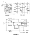
- Figure 1 is a block diagram of a prior art phase detector circuit.
- FIG. 2 is a block diagram of a phase-locked loop circuit incorporating a phase detector designed in accordance with the present invention.
- Figure 3 is a logic-level diagram of a preferred embodiment of the phase detector of the present invention.
- Figure 4 depicts a master-slave D flip-flop circuit used in the preferred embodiment.
- Figure 5 is a timing diagram depicting the operation of the circuit in Figure 4.
- Figure 6 is a simplified schematic diagram of a circuit that is logically equivalent to the circuit of Figure 3.
- FIGS 7 through 10 are timing diagrams depicting the operation of the circuit in Figure 3.
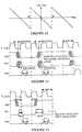
- Figure 11 shows the phase detector's transfer characteristics.
- Figure 12 is a phase detector timing diagram for an NRZI data stream with jitters.
- Figure 13 is a phase detector timing diagram for an NRZI data stream with duty cycle distortion.
- FIG 14 is a block diagram of a phase error processing circuit which processes the proportionate phase error information generated by the phase detector in Figure 2.
- a high frequency, clock/data recovery phase-locked loop (PLL) 100 The function of the PLL 100 is to generate a periodic clock signal P_CLK which matches the frequency and phase of an incoming 125 megabit per second data signal D IN .
- the data signal D IN is a NRZI coded data signal.
- the primary components of the PLL 100 are as follows.
- a three-stage ring oscillator 102 generates three equally phase spaced high frequency clock signals C1 to C3 having a frequency f0 of about 250 megahertz.
- a waveform synthesizer 104 also called a Digital Signed Phase-to-Frequency Converter, generates three equally phase spaced low frequency control signals having frequency
- the waveform synthesizer 104 is a low cost triangular wave digital synthesizer which generates triangular waveforms. Waveform synthesizer 104 is described more completely in application serial no. 07/ , , filed April 5, 1991.
- a frequency controlled oscillator (FCO) 110 generates a clock signal PLL_CLK whose frequency is equal to f0 + f M , where f M is positive or negative in accordance with the sign of the quantity 2f IN - f0.
- the PLL_CLK clock signal is divided by two by circuit 114 to generate the P_CLK signal, which is a square-wave signal that should match the frequency f IN (of about 125 MHz) and phase of the data signal D IN .
- FCO 110 is described more completely in application serial no. 07/ , , filed , 1991.
- Phase error detector 150 continually compares the phase of the P_CLK clock signal with the phase of the input signal D IN .
- the phase detector 150 generates a phase error signal having two components, PD1 and PD2.
- PD1 and PD2 are processed by a phase error processing circuit 152 to produce up/down frequency adjustment signals U/D and DATA-VALID. After being filtered by a digital loop filter 153, these frequency adjustment signals are used to adjust the frequency f M of the control signals generated by the waveform synthesizer 104.
- the phase detector 150 uses identical circuit elements, with virtually no delay mismatch, to ensure sampling of incoming data at the optimum point. In addition to phase error information, the phase detector also generates a recovered data signal RXD and a recovered clock signal RXC.
- the phase detector 150 comprises eight cells, herein labelled CELL1 through CELL8.
- CELL1 through CELL6 are identical AND/OR circuits, and thus the signal delay T1-T6 through each of these cells is virtually identical.
- CELL7 and CELL8 are identical AND/OR circuits (connected to perform XOR functions) with virtually identical signal delays T7-T8.
- Each of the eight cells contains two AND gates 170-172, with their outputs connected to the inputs of an OR gate 174.
- the AND gates in CELL1 through CELL6 each have two inputs, while the AND gates in CELL7 and CELL8 each have three inputs.
- CELL1 is used as a one cell delay for the data signal D IN whose output is labelled BDIN
- CELL6 is used as a one cell delay for the phase-locked loop clock P_CLK whose output is labelled BP_CLK.
- CELL2 through CELL5 are connected as transparent latches. More particularly, CELL2 and CELL3 together form a master-slave D flip-flop 180 that is used to latch the incoming data signal D IN for one clock cycle, with the latched data signal output by the circuit being labelled RXD2. CELL4 and CELL5 form a second master-slave D flip-flop 182 that is used to latch the RXD2 data signal for one clock cycle, with the signal output by the circuit being labelled RXD4.
- flip-flop 180 is as follows.
- P_CLK low (see Figure 5) the current value of D IN is read by AND gate 170 and transferred by OR gate 174 to RXD1.
- P_CLK goes high, the latched data value (RXD1) is transferred to RXD2 via AND gate 176 in CELL3. Furthermore, the current value of RXD1 is fed back through AND gate 172 in CELL2 so as to hold the latched value.
- a similar feed-back path is used to maintain the value of RXD2.
- flip-flop 180 samples and captures the D IN signal.
- Flip-flop 182 samples and stores the output of flip-flop 180 at the next clock cycle, much like the next bit in a shift register.
- the transition is reflected at RXD2 after P_CLK goes high, and the outputs RXD2 and RXD4 of the two flip-flops 180 and 182 differ for one clock cycle.
- CELL7 generates the exclusive-OR of the BDIN and RXD2 signals, with the resulting signal being called PD1.
- PD1 the resulting signal
- each transition in the data signal D IN should occur one-half clock cycle before it is reflected in the RXD2 signal, resulting in a PD1 pulse with a width TW1 of one-half clock cycle. If there is a phase error such that data transitions in D IN lead or lag the falling edge of P_CLK, then the PD1 pulse will be longer or shorter than one-half clock cycle, respectively.
- CELL8 generates the exclusive-OR of "RXD2 AND BP_CLK” and "RXD4 AND BP_CLK” with the resulting signal being called PD2.
- RXD2 and RXD4 are not equal, the delayed clock signal BP_CLK is allowed to pass through CELL8, with a fixed pulse width TW2 that is equal to half the BP_CLK clock period.
- Figure 6 shows a circuit that is the logical equivalent of the phase detector circuit 150 shown in Figure 3.
- the propagation delays T1-T6 of CELL1 through CELL6 are approximately equal, as are the propagation delays T7-T8 of CELL7 through CELL8.
- identical circuit elements are used to ensure that the gate delay for D IN and P_CLK are equal to the "clock to Q" delay at RXD2 as well as RXD4 such that at zero phase error, the pulse width TW1 equals the pulse width TW2, which is half the P_CLK period. This arrangement ensures that P_CLK samples D IN at about the center of the data symbol.
- phase detector of the present invention minimizes static alignment errors (SAE).
- SAE static alignment errors
- FIGS 7 and 8 are timing diagrams of the operation of phase detector 150 for negative and positive data transitions, respectively, which represent logic "1" symbols for NRZI data.
- the phase error for the negative data signal transition is denoted ⁇ E1 and the phase error for the positive data signal transition is denoted ⁇ E2.
- Each half-cycle of the P_CLK signal has a duration of four nanoseconds (assuming that P_CLK is running at 125 MHz).
- T1 to T8 Delays associated with the cells shown in Figure 3 are shown in these figures by time values T1 to T8.
- the width of each PD2 pulse is one-half clock cycle, shown as TW2.
- the width of each PD1 pulse which varies in accordance with phase error between the data signal D IN and the clock signal P_CLK, is shown as TW1A and TW1B (for negative and positive data transitions, respectively).
- ⁇ E1 is equal to 1.2 nanoseconds and ⁇ E2 is equal to 1.4 nanoseconds. If the cells have equal delays of about one nanosecond, TW1A is equal to about 2.8 nanoseconds, TW1B is equal to about 2.6 nanoseconds, and TW2 is equal to about 4.0 nanoseconds.
- RXD2 follows transitions in D IN with a delay of T3 after the next positive transition of P_CLK.
- RXD4 follows RXD2 a full clock cycle later.
- the delay from D IN to RXD4 is about one and half clock cycles.
- Recovered NRZI data signal RXD4 should be sampled at each negative transition of the recovered clock signal BP_CLK, such as points 300 and 302.
- each transition in the data signal D IN should occur simultaneously with the negative transition of P_CLK. If there is a phase error such that data transitions in the data signal D IN either leads or lags the negative transition during the P_CLK clock cycle, then the PD1 pulse will be either longer or shorter than one-half clock cycle. In the examples shown in Figures 7 and 8, the data signal lags the P_CLK negative transition, which means that clock is running a little too fast. As a result, the PD1 pulse is shorter than the PD2 pulse by an amount that is proportional to the phase error. When this phase error information is processed, the PLL's clock rate will be decreased slightly, causing the edges of the P_CLK signal to catch up to the transitions in the D IN signal. Note that when a transition in the data signal leads the P_CLK negative transition, which means that clock is running a little too slow, the PD1 pulse will be longer than the PD2 pulse by an amount that is proportional to the phase error.
- Figures 9 and 10 show two possible cases of a data stream representing logic "0" symbols for NRZI data. These figures show that no PD1 and PD2 pulses are generated when there are no transitions in the data stream D IN .
- the frequency of the clock signal P_CLK generated by the FCO (see Figure 1) is left unchanged.
- phase error K (TW1A - TW2)
- ⁇ E2 K (TW1B - TW2)
- Figure 12 shows the timing diagram of the phase detector for an NRZI data stream at D IN with jitters.
- the phase error information generated by the phase detector causes the PLL to adjust the phase of its clock P_CLK so that the average of TW1A+TW1B equals 2TW2.
- P_CLK will bephase-locked to the statistical mean of the jitters such that the phase error ⁇ E, on average, equals zero.
- Figure 13 shows the timing diagram of the phase detector with an NRZI data stream at D IN with duty cycle distortion.
- the pulse widths TW1A for one type of transition e.g., negative transitions
- the pulse widths TW1B are lengthened for the opposite type of transition (e.g., positive transitions).
- the phase error processor 152 of the present invention averages the phase error of adjacent positive and negative transitions and thereby enables the PLL to be locked to the statistical center of the "eye opening".
- identical circuit cells in the present invention ensures minimum distortion in the PD1 and PD2 pulse widths.
- identical circuit elements in CELL1, CELL3, CELL5 and CELL6 ensure that both TW1 and TW2 equal one half of the P_CLK clock cycle when the PLL is locked virtually at the optimum center of the eye-opening.
- the pulse width of PD1 does not approach zero, but rather approaches that of PD2, which is equal one half of the P_CLK clock cycle (e.g., 4 nanoseconds for a 125 MHz data signal).
- This arrangement provides sufficient pulse width for downstream logic gates, avoiding the dead-band problem associated with some prior art phase detectors that generate a pulse signal with zero pulse width when there is no phase error.
- the phase error information generated by the present invention is self contained in that it already includes a reference value (i.e., the width of PD2) for locking.
- the phase error processor 152 is used to process the PD1 and PD2 pulse signals from the phase detector 150.
- interface 158 allows the phase error information from two successive data transitions to propagate to the phase error integrator 160. While that information is being processed, the interface 158 blocks any further phase information from being applied to the integrator 160.
- the pulse widths of the PD1 and PD2 signals are integrated (or averaged) on two capacitors, 154 and 156. The accumulated voltages on the two capacitors due to the two successive PD1 and PD2 pulses correspond to the averaged phase error of the adjacent positive and negative data transitions.
- Comparator 162 determines the sign of the difference between the two integrated voltages, which indicates the sign of the average phase error due to successive positive and negative data transitions.
- the output of the comparitor 162 is a logic signal U/D (up/down) that instructs the waveform synthesizer and the FCO to either increase or decrease the frequency of the phase-locked clock P_CLK.
- interface 158 discharges the two integrating capacitors 154 and 156, and then the PD1 and PD2 phase error information from another pair of data transitions is processed in the next time frame.
- the phase error processor 152 disables its "Data-Valid" output signal so as to prevent unnecessary dithering of the phase-locked clock.
- the Data-Valid signal is enabled only when the processor 152 is ready to adjust the frequency of the phase-locked loop.
- Data-Valid is off, the frequency of the phase-locked loop is held at its current setting.
Applications Claiming Priority (2)
| Application Number | Priority Date | Filing Date | Title |
|---|---|---|---|
| US73022891A | 1991-07-15 | 1991-07-15 | |
| US730228 | 1991-07-15 |
Publications (1)
| Publication Number | Publication Date |
|---|---|
| EP0523885A1 true EP0523885A1 (fr) | 1993-01-20 |
Family
ID=24934487
Family Applications (1)
| Application Number | Title | Priority Date | Filing Date |
|---|---|---|---|
| EP92306098A Withdrawn EP0523885A1 (fr) | 1991-07-15 | 1992-07-01 | Détecteur de phase pour circuits de récupération d'informations et de l'horloge à haute fréquence |
Country Status (4)
| Country | Link |
|---|---|
| US (1) | US5329559A (fr) |
| EP (1) | EP0523885A1 (fr) |
| JP (1) | JPH05276028A (fr) |
| KR (1) | KR100234551B1 (fr) |
Cited By (4)
| Publication number | Priority date | Publication date | Assignee | Title |
|---|---|---|---|---|
| WO1996021973A1 (fr) * | 1995-01-11 | 1996-07-18 | National Semiconductor Corporation | Circuit processeur d'erreurs de phase avec technique de transfert alternee aux entrees d'un comparateur |
| EP0813153A2 (fr) * | 1996-06-14 | 1997-12-17 | Sun Microsystems, Inc. | Convertisseur série-parallèle dans un système de communication de données |
| EP0952669A1 (fr) * | 1998-03-12 | 1999-10-27 | Texas Instruments Incorporated | Dispositif de comparaison de phase |
| US7127017B1 (en) * | 2002-07-19 | 2006-10-24 | Rambus, Inc. | Clock recovery circuit with second order digital filter |
Families Citing this family (45)
| Publication number | Priority date | Publication date | Assignee | Title |
|---|---|---|---|---|
| US5831467A (en) | 1991-11-05 | 1998-11-03 | Monolithic System Technology, Inc. | Termination circuit with power-down mode for use in circuit module architecture |
| US5498990A (en) | 1991-11-05 | 1996-03-12 | Monolithic System Technology, Inc. | Reduced CMOS-swing clamping circuit for bus lines |
| DE69226150T2 (de) | 1991-11-05 | 1999-02-18 | Hsu Fu Chieh | Redundanzarchitektur für Schaltungsmodul |
| JPH08500687A (ja) * | 1992-08-10 | 1996-01-23 | モノリシック・システム・テクノロジー・インコーポレイテッド | ウェハ規模の集積化のためのフォルトトレラントな高速度のバス装置及びバスインタフェース |
| US5553275A (en) * | 1993-07-13 | 1996-09-03 | Intel Corporation | Method and apparatus for synchronously detecting phase relationships between a high-frequency clock and a low-frequency clock |
| US5619686A (en) * | 1993-11-18 | 1997-04-08 | National Semiconductor Corporation | Source synchronized data transmission circuit |
| US5655113A (en) | 1994-07-05 | 1997-08-05 | Monolithic System Technology, Inc. | Resynchronization circuit for a memory system and method of operating same |
| US5692023A (en) * | 1994-11-04 | 1997-11-25 | Lsi Logic Corporation | Phase locked loop including distributed phase correction pulses for reducing output ripple |
| US6239627B1 (en) * | 1995-01-03 | 2001-05-29 | Via-Cyrix, Inc. | Clock multiplier using nonoverlapping clock pulses for waveform generation |
| US6067102A (en) * | 1995-04-26 | 2000-05-23 | Hitachi, Ltd. | Electrophotographic recording device and exposure controlling device therefor |
| US5825824A (en) * | 1995-10-05 | 1998-10-20 | Silicon Image, Inc. | DC-balanced and transition-controlled encoding method and apparatus |
| US5999571A (en) * | 1995-10-05 | 1999-12-07 | Silicon Image, Inc. | Transition-controlled digital encoding and signal transmission system |
| US5974464A (en) * | 1995-10-06 | 1999-10-26 | Silicon Image, Inc. | System for high speed serial video signal transmission using DC-balanced coding |
| US5684805A (en) * | 1995-11-30 | 1997-11-04 | Brown; Anthony Kevin Dale | Microwave multiphase detector |
| JPH09292477A (ja) * | 1995-12-29 | 1997-11-11 | Council Scient Ind Res | 電話回線を介して標準時刻を送受信可能なマスタ−/スレイブ・クロック装置 |
| US5778217A (en) * | 1996-04-02 | 1998-07-07 | Lite-On Communications Corp. | Parallel signal processing device for high-speed timing |
| US6088415A (en) * | 1998-02-23 | 2000-07-11 | National Semiconductor Corporation | Apparatus and method to adaptively equalize duty cycle distortion |
| US6064235A (en) * | 1998-03-18 | 2000-05-16 | International Business Machines Corporation | Shared path phase detector |
| US6577694B1 (en) * | 1999-11-08 | 2003-06-10 | International Business Machines Corporation | Binary self-correcting phase detector for clock and data recovery |
| US6987817B1 (en) * | 2000-07-17 | 2006-01-17 | Lsi Logic Corporation | Digital clock recovery PLL |
| US20020093986A1 (en) * | 2000-12-30 | 2002-07-18 | Norm Hendrickson | Forward data de-skew method and system |
| WO2002054648A2 (fr) * | 2000-12-30 | 2002-07-11 | Vitesse Semiconductor Corporation | Procede et systeme de correction d'obliquite de donnees |
| US20020090045A1 (en) * | 2001-01-10 | 2002-07-11 | Norm Hendrickson | Digital clock recovery system |
| WO2002062004A1 (fr) | 2001-02-01 | 2002-08-08 | Vitesse Semiconductor Corporation | Recuperation de donnees rz |
| US7366267B1 (en) * | 2001-03-07 | 2008-04-29 | Altera Corporation | Clock data recovery with double edge clocking based phase detector and serializer/deserializer |
| US6509801B1 (en) | 2001-06-29 | 2003-01-21 | Sierra Monolithics, Inc. | Multi-gigabit-per-sec clock recovery apparatus and method for optical communications |
| US20040114702A1 (en) * | 2002-12-12 | 2004-06-17 | International Business Machines Corporation | Bang-bang phase detector for full-rate and half-rate schemes clock and data recovery and method therefor |
| US7505541B1 (en) | 2003-01-17 | 2009-03-17 | Xilinx, Inc. | NRZ/PAM-4/PRML triple mode phase and data detector |
| US6977959B2 (en) * | 2003-01-17 | 2005-12-20 | Xilinx, Inc. | Clock and data recovery phase-locked loop |
| US6956923B1 (en) * | 2003-01-17 | 2005-10-18 | Xilinx, Inc. | High speed phase detector architecture |
| US20040228411A1 (en) * | 2003-05-12 | 2004-11-18 | Sony Corporation | Method and system for decoder clock control in presence of jitter |
| JP3712401B2 (ja) * | 2003-06-16 | 2005-11-02 | 沖電気工業株式会社 | 光受信装置 |
| US7292670B2 (en) * | 2003-08-06 | 2007-11-06 | Gennum Corporation | System and method for automatically correcting duty cycle distortion |
| US7688887B2 (en) * | 2003-09-02 | 2010-03-30 | Gennum Corporation | Precision adaptive equalizer |
| US7089444B1 (en) | 2003-09-24 | 2006-08-08 | Altera Corporation | Clock and data recovery circuits |
| US7265690B2 (en) * | 2003-09-25 | 2007-09-04 | Texas Instruments Incorporated | Simplified data recovery from high speed encoded data |
| DE10345236B3 (de) * | 2003-09-29 | 2005-03-10 | Infineon Technologies Ag | Verzögerungsregelkreis |
| US7340660B2 (en) | 2003-10-07 | 2008-03-04 | International Business Machines Corporation | Method and system for using statistical signatures for testing high-speed circuits |
| US7200782B2 (en) * | 2003-10-23 | 2007-04-03 | Texas Instruments Incorporated | Clock recovery system for encoded serial data with simplified logic and jitter tolerance |
| US7119583B2 (en) * | 2004-03-31 | 2006-10-10 | Micron Technology, Inc. | Phase detector and method having hysteresis characteristics |
| US7512848B1 (en) * | 2004-09-29 | 2009-03-31 | Xilinx, Inc. | Clock and data recovery circuit having operating parameter compensation circuitry |
| US7751436B2 (en) * | 2005-05-24 | 2010-07-06 | Sony Corporation | System and method for dynamically establishing PLL speed based on receive buffer data accumulation for streaming video |
| US7423456B2 (en) * | 2006-12-01 | 2008-09-09 | Micron Technology, Inc. | Fast response time, low power phase detector circuits, devices and systems incorporating the same, and associated methods |
| US8509094B2 (en) * | 2007-12-06 | 2013-08-13 | Rambus Inc. | Edge-based loss-of-signal detection |
| US8630382B2 (en) * | 2009-03-27 | 2014-01-14 | Freescale Semiconductor, Inc. | Asynchronous data recovery methods and apparatus |
Citations (3)
| Publication number | Priority date | Publication date | Assignee | Title |
|---|---|---|---|---|
| GB2091961A (en) * | 1981-01-12 | 1982-08-04 | Sangamo Weston | Phase tolerant bit synchronizer for digital signals |
| US4371974A (en) * | 1981-02-25 | 1983-02-01 | Rockwell International Corporation | NRZ Data phase detector |
| EP0402711A1 (fr) * | 1989-06-15 | 1990-12-19 | Siemens-Albis Aktiengesellschaft | Dispositif pour la régénération d'un signal d'horloge avec une phase correcte |
Family Cites Families (8)
| Publication number | Priority date | Publication date | Assignee | Title |
|---|---|---|---|---|
| JPS58182938A (ja) * | 1982-04-21 | 1983-10-26 | Toshiba Corp | Pll形タイミング抽出回路 |
| US4584695A (en) * | 1983-11-09 | 1986-04-22 | National Semiconductor Corporation | Digital PLL decoder |
| US4635277A (en) * | 1985-10-21 | 1987-01-06 | Rockwell International Corporation | Digital clock recovery circuit apparatus |
| JP2718664B2 (ja) * | 1986-05-23 | 1998-02-25 | 株式会社日立製作所 | 位相同期検出回路 |
| GB2222751B (en) * | 1988-03-29 | 1992-08-26 | Plessey Co Plc | Clock driven data sampling circuit |
| KR920003598B1 (ko) * | 1988-12-22 | 1992-05-04 | 재단법인 한국전자통신 연구소 | Nrz비트 동기방식의 주파수 및 위상검출회로 |
| GB8924202D0 (en) * | 1989-10-27 | 1989-12-13 | Ncr Co | Digital phase lock loop decoder |
| KR930007716B1 (ko) * | 1990-07-20 | 1993-08-18 | 재단법인 한국전자통신연구소 | 비트 동기를 위한 디지틀 위상 검출기 |
-
1992
- 1992-07-01 EP EP92306098A patent/EP0523885A1/fr not_active Withdrawn
- 1992-07-14 KR KR1019920012499A patent/KR100234551B1/ko not_active IP Right Cessation
- 1992-07-14 JP JP18712392A patent/JPH05276028A/ja active Pending
-
1993
- 1993-03-04 US US08/026,266 patent/US5329559A/en not_active Expired - Lifetime
Patent Citations (3)
| Publication number | Priority date | Publication date | Assignee | Title |
|---|---|---|---|---|
| GB2091961A (en) * | 1981-01-12 | 1982-08-04 | Sangamo Weston | Phase tolerant bit synchronizer for digital signals |
| US4371974A (en) * | 1981-02-25 | 1983-02-01 | Rockwell International Corporation | NRZ Data phase detector |
| EP0402711A1 (fr) * | 1989-06-15 | 1990-12-19 | Siemens-Albis Aktiengesellschaft | Dispositif pour la régénération d'un signal d'horloge avec une phase correcte |
Cited By (5)
| Publication number | Priority date | Publication date | Assignee | Title |
|---|---|---|---|---|
| WO1996021973A1 (fr) * | 1995-01-11 | 1996-07-18 | National Semiconductor Corporation | Circuit processeur d'erreurs de phase avec technique de transfert alternee aux entrees d'un comparateur |
| EP0813153A2 (fr) * | 1996-06-14 | 1997-12-17 | Sun Microsystems, Inc. | Convertisseur série-parallèle dans un système de communication de données |
| EP0813153A3 (fr) * | 1996-06-14 | 2000-12-13 | Sun Microsystems, Inc. | Convertisseur série-parallèle dans un système de communication de données |
| EP0952669A1 (fr) * | 1998-03-12 | 1999-10-27 | Texas Instruments Incorporated | Dispositif de comparaison de phase |
| US7127017B1 (en) * | 2002-07-19 | 2006-10-24 | Rambus, Inc. | Clock recovery circuit with second order digital filter |
Also Published As
| Publication number | Publication date |
|---|---|
| JPH05276028A (ja) | 1993-10-22 |
| US5329559A (en) | 1994-07-12 |
| KR100234551B1 (ko) | 1999-12-15 |
| KR930003584A (ko) | 1993-02-24 |
Similar Documents
| Publication | Publication Date | Title |
|---|---|---|
| US5329559A (en) | Phase detector for very high frequency clock and data recovery circuits | |
| US6628112B2 (en) | System and method for detecting phase offset in a phase-locked loop | |
| US4400667A (en) | Phase tolerant bit synchronizer for digital signals | |
| US5712580A (en) | Linear phase detector for half-speed quadrature clocking architecture | |
| US6914953B2 (en) | Multiphase clock recovery using D-type phase detector | |
| US5455540A (en) | Modified bang-bang phase detector with ternary output | |
| US5239561A (en) | Phase error processor | |
| EP1016218B1 (fr) | Discriminateur de phase permettant l'extraction rapide de signaux d'horloge a partir de signaux binaires aleatoires | |
| US4837781A (en) | Phase locked loop clock synchronizer and signal detector | |
| JP2004507963A (ja) | データ・アイ・トラッキングを用いたデータ復元 | |
| KR20080018502A (ko) | 선형 위상검출기 및 그것을 포함하는 클럭 데이터 복원회로 | |
| US7929654B2 (en) | Data sampling circuit and method for clock and data recovery | |
| US6496555B1 (en) | Phase locked loop | |
| EP1408643B1 (fr) | Détecteur de phase avec marge de temps améliorée | |
| US6819728B2 (en) | Self-correcting multiphase clock recovery | |
| US6868134B2 (en) | Method and apparatus for recovering a clock signal from an asynchronous data signal | |
| US7236551B2 (en) | Linear half-rate phase detector for clock recovery and method therefor | |
| KR19990031788A (ko) | 고속 비복귀 기록 데이터 복구장치 | |
| US6970020B1 (en) | Half-rate linear quardrature phase detector for clock recovery | |
| US20190214997A1 (en) | Clock and data recovery of sub-rate data | |
| CN1711691B (zh) | 具有均衡自动调节相位线路的锁相环 | |
| JP2002094494A (ja) | クロック回復回路 | |
| CA2774482C (fr) | Circuit d'echantillonnage de donnees et procede de recuperation d'horloge et de donnees | |
| JP2005150890A (ja) | 位相比較器、位相同期ループ回路、およびクロック・データ・リカバリ回路 | |
| EP4175215B1 (fr) | Circuit de récupération d'horloge, dispositif et procédé correspondants |
Legal Events
| Date | Code | Title | Description |
|---|---|---|---|
| PUAI | Public reference made under article 153(3) epc to a published international application that has entered the european phase |
Free format text: ORIGINAL CODE: 0009012 |
|
| AK | Designated contracting states |
Kind code of ref document: A1 Designated state(s): DE FR GB IT NL |
|
| 17P | Request for examination filed |
Effective date: 19930626 |
|
| 17Q | First examination report despatched |
Effective date: 19951013 |
|
| STAA | Information on the status of an ep patent application or granted ep patent |
Free format text: STATUS: THE APPLICATION IS DEEMED TO BE WITHDRAWN |
|
| 18D | Application deemed to be withdrawn |
Effective date: 19960424 |