US4635277A - Digital clock recovery circuit apparatus - Google Patents
Digital clock recovery circuit apparatus Download PDFInfo
- Publication number
- US4635277A US4635277A US06/789,541 US78954185A US4635277A US 4635277 A US4635277 A US 4635277A US 78954185 A US78954185 A US 78954185A US 4635277 A US4635277 A US 4635277A
- Authority
- US
- United States
- Prior art keywords
- signals
- signal
- data
- clock
- output
- Prior art date
- Legal status (The legal status is an assumption and is not a legal conclusion. Google has not performed a legal analysis and makes no representation as to the accuracy of the status listed.)
- Expired - Lifetime
Links
Images


Classifications
-
- G—PHYSICS
- G11—INFORMATION STORAGE
- G11B—INFORMATION STORAGE BASED ON RELATIVE MOVEMENT BETWEEN RECORD CARRIER AND TRANSDUCER
- G11B20/00—Signal processing not specific to the method of recording or reproducing; Circuits therefor
- G11B20/10—Digital recording or reproducing
- G11B20/14—Digital recording or reproducing using self-clocking codes
- G11B20/1403—Digital recording or reproducing using self-clocking codes characterised by the use of two levels
-
- H—ELECTRICITY
- H04—ELECTRIC COMMUNICATION TECHNIQUE
- H04L—TRANSMISSION OF DIGITAL INFORMATION, e.g. TELEGRAPHIC COMMUNICATION
- H04L7/00—Arrangements for synchronising receiver with transmitter
- H04L7/02—Speed or phase control by the received code signals, the signals containing no special synchronisation information
- H04L7/033—Speed or phase control by the received code signals, the signals containing no special synchronisation information using the transitions of the received signal to control the phase of the synchronising-signal-generating means, e.g. using a phase-locked loop
- H04L7/0337—Selecting between two or more discretely delayed clocks or selecting between two or more discretely delayed received code signals
Definitions
- the present invention is generally concerned with electronics and more specifically with a clock recovery circuit. Even more specifically, it is concerned with a digital version of a clock recovery circuit comprising a detection circuit for detecting the length of a pulse in combination with a nonlinear digital phase-locked loop.
- a typical prior art approach to detecting the appropriate time to generate a clock signal in response to received data which is of the type that is noncontinuous, was to use a resonant (ringing tank) clock circuit.
- the ringing tank required a minimum repetition rate of data pulses being received to keep the clock circuit in a "ringing" condition.
- these circuits were subject to temperature variations, and accordingly to drift in frequency of operation.
- these circuits required a considerable amount of testing and adjusting at the factory and later in the field to keep the devices tuned to the appropriate frequencies.
- the clock signals must occur at a prescribed time with respect to data being detected.
- a phase-locked loop circuit can then be operated at the high frequency clock rate to generate a new output signal representative of the data pulse, of the exact design length and having a clock situated at the optimal time with respect to the data pulse.
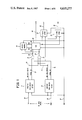
- FIG. 1 is a block diagram of the overall inventive concept
- FIG. 2 is a set of waveforms used in explaining the operation of FIG. 1;
- FIG. 3 is a block diagram of a portion of FIG. 1;
- FIGS. 4 through 9 are waveforms used in explaining the operation of the invention.
- FIG. 10 is a diagram used in explaining the operation of the sequencer
- FIG. 11 is a set of waveforms used in explaining the operation of the sequencer.
- FIG. 12 is a detailed schematic diagram of a portion of FIG. 1;
- FIG. 13 is a detailed schematic diagram of another portion of FIG. 1;
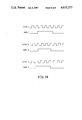
- FIG. 14 comprises a set of waveforms used in explaining the operation of FIGS. 1 and 3.
- a lead 10 which is also labeled TIP, supplies signals to a positive data center detect block 12.
- a RING lead 14 supplies signals to a negative data center detect block 16.
- the leads 10 and 14 comprise the return-to-zero data inputs.
- a clock signal is supplied on a lead 18 to both the blocks 12 and 16 as well as to a sequencer block 20, a resynchronization block 22, a negative data latch 24 and a positive data latch 26.
- Signals indicative of a detection of the data center are output from block 12 on a lead 28 to an OR gate 30 which receives similar signals from a lead 31 output by block 16.
- the lead 28 is also connected to supply signals to the positive data latch 26.
- lead 31 is also connected to negative data latch 24.
- Signals indicative of receipt of a normal length data center are output on a lead 32 from positive data center block 12 to an OR gate 34. Similar signals are output on a lead 36 from negative data center detect block 16 to another input of OR gate 34.
- the output signals of OR gate 30 are supplied on a lead 38 both to sequencer 20 and to resynchronization circuit 22. Output signals from OR gate 34 are supplied on a lead 40 to sequencer 20 as well as to resynchronization circuit 22.
- the resynchronization circuit 22 has leads 42 and 44 for indicating to sequencer 20 to operate on a divide-by-seven or divide-by-nine basis, respectively.
- the sequencer 20 also supplies output clock signals on a lead 46. Positive data signals are supplied on a lead 48 from latch 26, while negative data signals are supplied on lead 50 from negative data latch block 24.
- the waveform in FIG. 2a illustrates a bipolar tip-ring signal as carried on a typical telephone line.
- the waveform in 2b illustrates the unipolar return-to-zero signal indicative of when 2a is positive relative a ground reference.
- the waveform 2c indicates when the signal of 2a is negative.
- FIG. 3 illustrates the circuitry within either of the data center detect blocks 12 and 16.
- a shift register 54 which supplies a plurality of outputs labeled A through G to each of a set of decode blocks 56, 58 and 60. These blocks are labeled, respectively, long pulse decode, normal pulse decode and short pulse decode.
- the output of each of these blocks is supplied to an OR gate 62, which provides output signals on a lead 64 which would be comparable to leads 28 or 31 of FIG. 1.
- the output from block 58 is supplied on a lead 66 as an indication of a normal data center, and this would be similar to the signals appearing on leads 32 or 36 of FIG. 1.
- the shift register 54 comprises seven portions so that it can, at any given time, output seven contiguous bits of sampled data, but more samples could be obtained using a higher clock frequency for some applications.
- a waveform labeled CLOCK is illustrated which operates at eight times the frequency of the data pulse repetition rate.
- the data pulse can be sampled in the logic "1" condition either three or four times.
- the system is set up so that the delayed center of the incoming data pulse is phase locked to cycle C4 while the decoding point for the data center output occurs in cycle C8.
- the waveform labeled data in FIG. 4 is shown commencing just after the commencement of cycle C1 with a shaded portion extending to just prior to the end of cycle C1.
- the data pulse is shown as ending during cycle C7.
- the shaded portions are used to illustrate the possible variation in time of the actual received data pulse, while still producing the same length unipolar signal to be decoded as shown by waveforms A through G in FIG. 4.
- FIG. 4 illustrates a condition where the value of the signal in waveform A is a logic "0", but the remaining waveforms B through F are in a logic "1" condition and waveform G is a logic "0".
- FIG. 5 is a further illustration of a slightly narrower data pulse than that shown in FIG. 4. This data pulse commences during cycle C2 and ends during cycle C7. Shaded portions are used for the same reasons as in FIG. 4. During the decoding cycle C8 all the waveforms of FIG. 5 provide a logic "1" except those of waveforms A and G.
- FIG. 5, FIG. 6 and FIG. 7 together show the three possibilities for sampling of a normal length pulse.
- a normal pulse is defined as being more than three sampling periods, shown in FIG. 7, and less than six full sampling periods, as shown in FIG. 5.
- FIGS. 8 and 9 show the two possibilities for sampling of a short length pulse.
- a short pulse is defined as greater than one sampling period and less than three full sampling periods, examples of which are shown in FIGS. 8 and 7, respectively.
- FIG. 10 thirteen states are shown for the possible digital outputs of the sequencer 20 of FIG. 1.
- the output of the sequencer is shown within each one of the states S1 through S13.
- state S3 the first digit or the A digit (as presented in FIG. 13) is a logic "1" while the remaining digits B through D are logic "0".
- state S9 the A and B digits are logic "0" and the C and D digits are logic "1's”.
- the A digit is also used as the clock signal 46 in FIG. 1, and thus the output clock is a logic "1" in states S3 through S6 and states S11 and S12.
- the decoding circuitry within sequencer 20 determines the path and thus to which state an advance is made in the next clock cycle.
- DC data center input
- the signals P, N, CK are outputs of the circuit and are applied to leads 48, 50 and 46 of FIG. 1, respectively.
- the signals labeled Pn-1 and Nn-1, listed in the state blocks of FIG. 10, are the values of P and N in the previous state.
- the signals RS7 and RS9 are the outputs of internal memory devices that hold the resync mode (the path or steps to be taken if resynchronization is required) of the sequencer until acted upon.
- the PR label indicates that the output that it is paired with has the value given in the accompanying equation during that state.
- the output P has the value Pn-1 that it had at the end of state S1 (the previous state) from the beginning of S2 to the end of S2.
- the output CK has the logical value "0".
- the term “Reset” indicates a logic value "0", while “Set” indicates the logic value "1".
- the typical path is S8, S1, S2, S3, S4, S5, S6, S7 and back to S8. If there is jitter or variations in the time of occurrence of the data centers, the data center input to the sequence can occur in states S6, S7, S8, S9, S10. If the data center occurs in one of these states, the exit path to S1 will be taken to return the data center to the time of occurrence of state S8. In other words, there is a dynamic adjustment during the time of receipt of logic "1's" in a phase-locked loop manner. When the data center logic "1's" are not received, the normal path is S8, S9, S10, S11, S12, S5, S6, S7 and back to S8.
- the state sequence is adjusted by either shortening the sequence to seven states by branching from state S9 to state S11 or extending the sequence to 9 states by branching from state S13 to state S11 to return the received normal data centers to the time of occurrence associated with state S8.
- waveforms A and B represent respectively the tip and ring (RZ) signals.
- Waveform C illustrates the signal appearing on a lead indicating the receipt of a positive data center as opposed to a negative data center, while the waveform D represents the signal appearing on a data center lead such as 28 in FIG. 1.
- the sequencer 20 would follow that sequence shown in the state sequence of FIG. 11e from states S1 through S8.
- An output, such as on lead 48 of FIG. 1, would appear as shown in waveform F commencing at the start of state S1 and ending at the end of state S4.
- a clock signal illustrated in waveform G of FIG. 11 would be similarly output on lead 46 of FIG. 1.
- the clock signal of waveform G commences at the start of state S3 and continues to the end of state S6.
- no data center is detected and thus there is no logic "1" output in waveform F, however, the clock signal of waveform G again occurs commencing at state 11 of the presentation in line E of FIG. 11.
- the second sequence from S9 through S12 and then S5 to S8 is repeated as long as no further data centers are detected.
- FIG. 12 shows a detailed six tap schematic diagram which allows slightly more errors in detection than would be associated with the seven tap scheme shown in the other drawings.
- the addition to this drawing for seven taps would be obvious to one skilled in the art.
- the inclusion herein of the additional gates necessary to show a seven tap schematic would merely clutter up the drawing and make it harder to understand the detailed concept.
- the upper portion illustrates the positive data center detect block 12 of FIG. 1 and comprises a shift register 65 and a plurality of NAND and OR gates, generally designated as 67.
- the lower portion of FIG. 12 illustrates the block 16 and comprises a shift register 69 and a plurality of NAND and OR gates 71.
- the outputs of the sets of gates 67 and 71 are logically combined in a set of D flip-flops, generally designated as 73, which provide the outputs of positive data center on lead 75, inverse normal data center (DCN) on lead 77, a data center of any type on lead 79 and a negative data center on lead 81.
- DCN inverse normal data center
- a further inverse data center (DC) is illustrated as being supplied on lead 83.
- FIG. 13 has a set of input leads using the same designations as those output by FIG. 12 and includes in addition a clock 85.
- the upper left hand portion of FIG. 13 comprises the resynchronizing portion designated as 22 in FIG. 1, while a majority of the remainder including the JK flip-flops comprises the sequencer 20.
- the right hand portion coaprises the positive data and negative data latches 24 and 26 with the signals being combined in a NOR gate 87 and combined for output as return-to-zero data.
- the retimed clock output is given the same designation as in FIG. 1.
- FIG. 14 comprises three sets of clock and data signals. These three sets are used to illustrate the movement of the data pulse with respect to the clock pulse. Such a movement of the data pulse with respect to the clock pulse would normally take place over a long period of time. Thus, the illustrations are shown as separate instances in FIG. 14 with each data pulse being illustrated with respect to a corresponding portion of the clock stream. Further, the data pulse widths are presented as being different to illustrate that the data pulse is not always the same duration. As illustrated, the data is lagging the rising edge of the clock pulse for data 1 and is leading by a lesser amount at the time indicated for data 2 while the data leads the clock pulse in the instance shown for data 3.
- the present invention was designed specifically to work with telephonetype signals wherein the tip or ring signals are pulses which nominally are 320 nanoseconds in length and are separated in logic data bit values by 320 nanoseconds. This would be the normal length pulse as shown in FIGS. 5, 6 or 7, as well as FIG. 2.
- the sampling clock used in one embodiment of the invention thus operated at 12.352 MHz and for the nominal length pulse provided four samples of the signal itself and four samples of the separation time. This is illustrated in FIG. 11, waveforms E through G. Modifications to allow operation at other frequencies will be apparent to those skilled in the art.
- the purpose of the present invention is to generate (or recover) a clock signal which would occur at a time such that it could be used in timing other circuitry from an incoming signal which did not contain the clock, and which at times did not have any logic "1" excursions of the incoming signal.
- the absence of logic "1" excursions of the amplitude of the incoming signal of the prior art tended to allow the ringing tank circuits used in the prior art to drift substantially in clock frequency from the desired frequency and to thus make errors in the detection of incoming data.
- FIG. 3 in combination with explanatory FIGS. 4 through 9.
- FIG. 3 shows a block diagram of the data center detection circuit.
- the purpose of this circuit is to generate signals that: (1) indicate the approximate center of an incoming data pulse, and, (2) indicate the type or length of that data pulse.
- the length of the incoming signal is determined by the number of cycles of the clock signal, shown in FIG. 3, which occur during the presence of an incoming data pulse. This purpose is complicated by the fact that the time of the beginning of the clock signal and the beginning of the data signal have no set or predetermined relationship. This is shown in FIG. 14.
- a further practical restriction requires that for data to be entered into the shift register, it must be a defined logic level for a specified minimum amount of time before the beginning of a clock cycle.
- the center of a data pulse is determined by allowing the incoming data pulse to be sampled, or entered, into the shift register until the end of the data pulse is detected. By doing so, the time of occurrence of the beginning and end of the pulse is known and the center can therefore be determined.
- the clock signal operates at eight times the given nominal frequency of the incoming signal. This implies that the normal data pulse width is four clock cycles in length.
- FIG. 6 shows an incoming data pulse of exactly four clock cycles in length.
- the Figure also indicates that the data pulse has reached a logic "1" value before the beginning of clock cycle S2 and has reached a logic "0" value before the beginning of clock cycle S7.
- Four clock cycles have occurred during the presence of the data pulse and each of the signals A-G are logic "1's" for four clock cycles.
- the center of this incoming data pulse is during S4. It should be noted that any pulse which begins during S2 cycle and ends during S7 is interpreted in the above manner, although the pulse just described could be only slightly larger than three clock cycles or slightly less than five full clock cycles. This is decoded at the output of the shift register during S8 as being a normal length pulse.
- FIG. 5 shows an input pulse whose length is only slightly larger than four clock cycles but less than six full clock cycles
- FIG. 7 shows an input pulse whose length is less than four full clock cycles but more than two clock cycles. Since small variations in the frequency of the input pulses are acceptable, and hence variations in the pulse length, both FIGS. 5 and 7 are also interpreted as being normal width pulses. This interpretation would appear to allow for a large variation in a "normal" pulse, but close examination will prove that this is not the case.
- FIG. 5 indicates that the signal would be interpreted as a normal length pulse. But further assume that the shifting described by FIG. 14 occurred, then as shown in FIG. 4, the pulse would be interpreted correctly as a long pulse. The same relationship is apparent between FIGS. 7 and 8 for normal and short pulses.
- a normal length pulse can be defined as being less that six full clock cycles in length and greater than three clock cycles (see FIG. 7) in length.
- a long pulse is defined as less than seven full but more than five clock cycles.
- a short pulse is defined as at least one clock cycle and less than two full clock cycles.
- the apparatus of FIG. 3 is included in the block 12 for positive signals in FIG. 1 and in block 16 for negative signals.
- the block 12 of FIG. 1 thus detects logic "1's" present in the tip return-to-zero data and the block 16 detects logic "1's” present in the ring return-to-zero data.
- These signals are combined and applied to the sequencer 20.
- the sequence followed in transversing the states of FIG. 10 is determined in accordance with a plurality of inputs. As shown in FIG. 1, this plurality of inputs includes the occurrence of data center pulses and clock signals.
- the resynchronization block 22 starts adjusting the sequencer output to a value such that clock cycle C8 as shown in FIG. 4, which is the decoding point, falls substantially in the center of the continuously received but flip-flop time delayed normal length data pulses.
- the resynchronization circuit 22 is used only for power-up synchronization and noise filtering, since the sequencer itself can dynamically adjust for slow alterations in the incoming data signal, and can hold the clock at a stable value over a long period of time without the occurrence of any logic "1" or logic "0" signals being received.
- states are the values of the Q outputs of JK flip-flops A through D in FIG. 13, generally indicated as 20.
- the exit path from a given state is controlled by input signals received by the sequencer during that state. For example, if any data center is input to the sequencer in S8, then it will branch to S1 as shown by the line, otherwise it will branch to S9 at the beginning of the next clock cycle. Similarly, in S9 if a data center is received during that state it will branch to S1. However, if no data center is received, and a normal length data center was received at a time other than that of S1 through S6 in the previous cycle, the device will branch to state S11. If neither of the other two signal conditions occurred, it will branch to S10.
- the two main paths through the state sequence unit 20 are (1) states S8, S1, S2, S3, S4, S5, S6, S7 and return to the sequence starting with S8 and (2) states S11, S12, S5, S6, S7, S8, S9, S10 and return to S11.
- the first sequence is for the times when a data center is received during the times S7 through S9, and the other is when no normal length data center is received during the times S7 through S9.
- an output clock will be generated starting 2 clocks before state S5 or in other words, if no data center is received, the clock will start at state S11 and if a data center is received, the clock will start at state S3.
- the leftmost bit in each case is a logic "1", and this is decoded from the output of the A flip-flop in FIG. 13, and output as the retimed clock signal on lead 46.
- a data center When a data center occurs, it occurs at a maximum rate of 1.544 MHz for the application being referenced.
- the data center typically or nominally lasts 80.97 nanoseconds in one application of the inventive concept.
- the data center is synchronous with the transition from state to state in the sequencer 20 and in normal operation it occurs during state S8. When the data center is detected in state S8, the following occurs:
- phase jitter produces phase accumulation offsets, over a long period of time it has an average zero value.
- the two sources of phase deviation may be additive and are treated as one source of jitter in this presentation.
- each of the states S6, S8, S9 and S10 have an exit path to S1. If the frequency of the clock divided by 8, or whatever the sampling rate might be, is not equal to the frequency of the data pulse, there will be a change in the zero phase point. If the clock divided by the number of samples is a value greater than the average nominal data frequency, the phase of the center of state S8 will slowly shift with respect to the center of the data pulse. If the data pulse shifts to the right in FIG. 6, the data center will eventually be detected in S9. If the normal pulse is detected then, the path from state S9 to State S1 is followed and in effect has divided the clock by 9 rather than the normal 8. This will shift the center of the data pulse back to the S8 condition on the next cycle.
- the incoming signal is allowed to contain as many as 15 time intervals where no data (or zero data) is transmitted. During this amount of time, it is highly probable that phase jitter, which can accumulate although no data is transmitted, would cause the time of occurrence of the signal data center to drift from state 8 of FIG. 10 through state 9 and finally into state 10 before a data pulse was received. If a branch between S10 and S1 was not provided, a data error (incorrectly interpreted data) would occur. Similarly, the signal data center could drift from state S8 through S7 and into S6 necessitating a branch from S6 to S1.
- this device is a nonlinear digital phase-locked loop having discrete phase c adjustment steps of 2 ⁇ /8 radians.
- the resynchronization circuit 22 of FIG. 1 performs the two functions of noise filtering and synchronization for power-up or after a loss of signal.
- the data center can occur at any state of the sequencer 20.
- the objective of the resynchronization circuit 22 is to force state S8 to occur simultaneously with the data center signal. If the data center is found to occur in S1, S2, S3, S11 or S13 the path taken is through S9, S10 and S13 back to S11 to advance the phase of the output clock. On the other hand, if the data center if found to occur in S4, S5 or S12, the path taken is from S8 and S9 directly to S11 to "lag" the phase of the output clock.
- the resynchronization circuit 22 will only make one adjustment per normal data center. In other words, any pulses other than a normal pulse could be noise, and thus are ignored during the resynchronization process. This, in effect, filters the noise pulses since only normal length pulses can cause the resynchronization action.
- FIGS. 12 and 13 presents a specific embodiment for ring and tip signals used in a telephone line having return-to-zero input and output. Since the design is reasonably straightforward, it is believed that further explanation of the specific circuit used is unnecessary. Further, it will be realized by those skilled in the art that other sampling rates could be used to obtain more accuracy, or in other words, smaller steps in the adjustment of the phase-locked loop.
Landscapes
- Engineering & Computer Science (AREA)
- Signal Processing (AREA)
- Computer Networks & Wireless Communication (AREA)
- Synchronisation In Digital Transmission Systems (AREA)
Abstract
Description
______________________________________
State Notation
______________________________________
S8    the data center is detected so it branches to state S1.
S1    the pulse center either negative or positive, which caused
      the data center to be detected is latched to the
      appropriate output.
S2    the data output is maintained.
S3    the clock is driven to a logic "1" while the data level is
      maintained.
S4    the data and clock levels are maintained.
S5    the clock is maintained while the data is driven to a logic
      "0", whether it be a positive or negative data center.
S6    the clock and data levels are maintained
S7    the clock is driven to a logic "0" while the data level is
      maintained.
S8    in normal operation, if another logic "1" is present in the
      input data, the data center will occur here and the
      sequence repeats.
______________________________________
Claims (5)
Priority Applications (1)
| Application Number | Priority Date | Filing Date | Title |
|---|---|---|---|
| US06/789,541 US4635277A (en) | 1985-10-21 | 1985-10-21 | Digital clock recovery circuit apparatus |
Applications Claiming Priority (1)
| Application Number | Priority Date | Filing Date | Title |
|---|---|---|---|
| US06/789,541 US4635277A (en) | 1985-10-21 | 1985-10-21 | Digital clock recovery circuit apparatus |
Publications (1)
| Publication Number | Publication Date |
|---|---|
| US4635277A true US4635277A (en) | 1987-01-06 |
Family
ID=25147929
Family Applications (1)
| Application Number | Title | Priority Date | Filing Date |
|---|---|---|---|
| US06/789,541 Expired - Lifetime US4635277A (en) | 1985-10-21 | 1985-10-21 | Digital clock recovery circuit apparatus |
Country Status (1)
| Country | Link |
|---|---|
| US (1) | US4635277A (en) |
Cited By (16)
| Publication number | Priority date | Publication date | Assignee | Title |
|---|---|---|---|---|
| US4873700A (en) * | 1987-10-14 | 1989-10-10 | National Semiconductor Corporation | Auto-threshold/adaptive equalizer |
| US4888790A (en) * | 1987-10-14 | 1989-12-19 | National Semiconductor Corp. | Timing recovery system using bipolar-pattern center estimator |
| US4912726A (en) * | 1987-01-12 | 1990-03-27 | Fujitsu Limited | Decision timing control circuit |
| US4928289A (en) * | 1988-12-19 | 1990-05-22 | Systran Corporation | Apparatus and method for binary data transmission |
| US5054020A (en) * | 1990-04-11 | 1991-10-01 | Digital Access Corporation | Apparatus for high speed data communication with asynchronous/synchronous and synchronous/asynchronous data conversion |
| US5063576A (en) * | 1988-12-28 | 1991-11-05 | Nec Corporation | Coding and decoding method for asynchronous data signals and an apparatus therefor |
| EP0479176A1 (en) * | 1990-09-29 | 1992-04-08 | Anritsu Corporation | Waveform shaping circuit and digital signal analyzing apparatus using the same |
| US5239561A (en) * | 1991-07-15 | 1993-08-24 | National Semiconductor Corporation | Phase error processor |
| US5329559A (en) * | 1991-07-15 | 1994-07-12 | National Semiconductor | Phase detector for very high frequency clock and data recovery circuits |
| US5592519A (en) * | 1994-06-22 | 1997-01-07 | Alcatel Network Systems, Inc. | Dual frequency clock recovery using common multitap line |
| US5596331A (en) * | 1988-05-13 | 1997-01-21 | Lockheed Martin Corporation | Real-time control sequencer with state matrix logic |
| US5671259A (en) * | 1995-08-24 | 1997-09-23 | Northern Telecom Limited | Clock recovery circuit |
| US5689530A (en) * | 1994-06-22 | 1997-11-18 | Alcatel Network Systems, Inc. | Data recovery circuit with large retime margin |
| US5694435A (en) * | 1993-12-23 | 1997-12-02 | Deutsche Aerospace Ag | Digital method of detecting pulses of short duration and arrangement for implementing the method |
| WO2004106673A1 (en) * | 2003-05-30 | 2004-12-09 | Zhuyu Gao | Application method of machine logic, device of machine logic and digital lock of machine logic |
| US20070291888A1 (en) * | 2006-06-20 | 2007-12-20 | Ciena Corporation | System and method for an adaptable timing recovery architecture for critically-timed transport applications |
Citations (3)
| Publication number | Priority date | Publication date | Assignee | Title |
|---|---|---|---|---|
| US4412339A (en) * | 1981-09-24 | 1983-10-25 | Advanced Micro Devices, Inc. | Zero-crossing interpolator to reduce isochronous distortion in a digital FSK modem |
| US4571514A (en) * | 1982-11-26 | 1986-02-18 | Motorola, Inc. | Amplitude adjusted pulse width discriminator and method therefor |
| US4571735A (en) * | 1981-10-08 | 1986-02-18 | Furse Anthony G | Method of multi-level encoding including synchronizing signals |
-
1985
- 1985-10-21 US US06/789,541 patent/US4635277A/en not_active Expired - Lifetime
Patent Citations (3)
| Publication number | Priority date | Publication date | Assignee | Title |
|---|---|---|---|---|
| US4412339A (en) * | 1981-09-24 | 1983-10-25 | Advanced Micro Devices, Inc. | Zero-crossing interpolator to reduce isochronous distortion in a digital FSK modem |
| US4571735A (en) * | 1981-10-08 | 1986-02-18 | Furse Anthony G | Method of multi-level encoding including synchronizing signals |
| US4571514A (en) * | 1982-11-26 | 1986-02-18 | Motorola, Inc. | Amplitude adjusted pulse width discriminator and method therefor |
Cited By (23)
| Publication number | Priority date | Publication date | Assignee | Title |
|---|---|---|---|---|
| US4912726A (en) * | 1987-01-12 | 1990-03-27 | Fujitsu Limited | Decision timing control circuit |
| US4888790A (en) * | 1987-10-14 | 1989-12-19 | National Semiconductor Corp. | Timing recovery system using bipolar-pattern center estimator |
| JPH02153629A (en) * | 1987-10-14 | 1990-06-13 | Natl Semiconductor Corp <Ns> | Timing recovery system using bipolar pattern center estimator |
| EP0311974A3 (en) * | 1987-10-14 | 1991-05-15 | National Semiconductor Corporation | Timing recovery system using bipolar-pattern center estimator |
| JP2852932B2 (en) | 1987-10-14 | 1999-02-03 | ナショナル セミコンダクタ コーポレーション | Bipolar pattern center estimator |
| US4873700A (en) * | 1987-10-14 | 1989-10-10 | National Semiconductor Corporation | Auto-threshold/adaptive equalizer |
| US5596331A (en) * | 1988-05-13 | 1997-01-21 | Lockheed Martin Corporation | Real-time control sequencer with state matrix logic |
| US4928289A (en) * | 1988-12-19 | 1990-05-22 | Systran Corporation | Apparatus and method for binary data transmission |
| WO1990007242A1 (en) * | 1988-12-19 | 1990-06-28 | Systran Corporation | Apparatus and method for binary data transmission |
| US5063576A (en) * | 1988-12-28 | 1991-11-05 | Nec Corporation | Coding and decoding method for asynchronous data signals and an apparatus therefor |
| US5054020A (en) * | 1990-04-11 | 1991-10-01 | Digital Access Corporation | Apparatus for high speed data communication with asynchronous/synchronous and synchronous/asynchronous data conversion |
| US5210712A (en) * | 1990-09-29 | 1993-05-11 | Anritsu Corporation | Waveform shaping circuit and digital signal analyzing apparatus using the same |
| EP0479176A1 (en) * | 1990-09-29 | 1992-04-08 | Anritsu Corporation | Waveform shaping circuit and digital signal analyzing apparatus using the same |
| US5329559A (en) * | 1991-07-15 | 1994-07-12 | National Semiconductor | Phase detector for very high frequency clock and data recovery circuits |
| US5239561A (en) * | 1991-07-15 | 1993-08-24 | National Semiconductor Corporation | Phase error processor |
| US5694435A (en) * | 1993-12-23 | 1997-12-02 | Deutsche Aerospace Ag | Digital method of detecting pulses of short duration and arrangement for implementing the method |
| US5592519A (en) * | 1994-06-22 | 1997-01-07 | Alcatel Network Systems, Inc. | Dual frequency clock recovery using common multitap line |
| US5689530A (en) * | 1994-06-22 | 1997-11-18 | Alcatel Network Systems, Inc. | Data recovery circuit with large retime margin |
| US5671259A (en) * | 1995-08-24 | 1997-09-23 | Northern Telecom Limited | Clock recovery circuit |
| WO2004106673A1 (en) * | 2003-05-30 | 2004-12-09 | Zhuyu Gao | Application method of machine logic, device of machine logic and digital lock of machine logic |
| CN1802485B (en) * | 2003-05-30 | 2013-10-16 | 高瞩宇 | Mechanical logic application method, mechanical logic device and mechanical logic digital lock |
| US20070291888A1 (en) * | 2006-06-20 | 2007-12-20 | Ciena Corporation | System and method for an adaptable timing recovery architecture for critically-timed transport applications |
| US7733999B2 (en) * | 2006-06-20 | 2010-06-08 | Ciena Corporation | System and method for an adaptable timing recovery architecture for critically-timed transport applications |
Similar Documents
| Publication | Publication Date | Title |
|---|---|---|
| US4635277A (en) | Digital clock recovery circuit apparatus | |
| EP0317159B1 (en) | Clock recovery arrangement | |
| US4361895A (en) | Manchester decoder | |
| EP0773653B1 (en) | Method and apparatus for decoding Manchester-encoded data | |
| EP0045749B1 (en) | Selfsynchronizing clock derivation circuit for double frequency encoded digital data | |
| US4837781A (en) | Phase locked loop clock synchronizer and signal detector | |
| JPS60227541A (en) | Digital phase locked loop type decoder | |
| US5491729A (en) | Digital phase-locked data recovery circuit | |
| US4017803A (en) | Data recovery system resistant to frequency deviations | |
| EP1599963B1 (en) | Clock and data recovery method and apparatus | |
| US5457428A (en) | Method and apparatus for the reduction of time interval error in a phase locked loop circuit | |
| WO1986003638A1 (en) | Clock recovery circuit | |
| US5550878A (en) | Phase comparator | |
| US5717728A (en) | Data/clock recovery circuit | |
| JPH088738A (en) | Pll circuit device | |
| US6794945B2 (en) | PLL for clock recovery with initialization sequence | |
| WO1999057842A1 (en) | Jitter measurement | |
| US6339833B1 (en) | Automatic recovery from clock signal loss | |
| WO1989006885A1 (en) | Data bit detector for fiber optic system | |
| US6891402B2 (en) | Clock's out-of-synchronism state detection circuit and optical receiving device using the same | |
| US5058142A (en) | Clock extracting circuit in digital-line signal receiver | |
| US4855735A (en) | Recovery of data clock signals | |
| WO1991018449A1 (en) | Scaler for synchronous digital clock | |
| US4464769A (en) | Method and apparatus for synchronizing a binary data signal | |
| WO2003081766A1 (en) | Detection of frequency differences between signals |
Legal Events
| Date | Code | Title | Description |
|---|---|---|---|
| AS | Assignment |
Owner name: ROCKWELL INTERNATIONAL CORPORATION Free format text: ASSIGNMENT OF ASSIGNORS INTEREST.;ASSIGNORS:BLAKE, JOHN K.;NELSON, BLAINE J.;REEL/FRAME:004471/0108 Effective date: 19851014 |
|
| STCF | Information on status: patent grant |
Free format text: PATENTED CASE |
|
| FEPP | Fee payment procedure |
Free format text: PAYOR NUMBER ASSIGNED (ORIGINAL EVENT CODE: ASPN); ENTITY STATUS OF PATENT OWNER: LARGE ENTITY |
|
| FPAY | Fee payment |
Year of fee payment: 4 |
|
| AS | Assignment |
Owner name: ALCATEL NETWORK SYSTEM INC., Free format text: ASSIGNMENT OF ASSIGNORS INTEREST.;ASSIGNOR:ROCKWELL INTERNATIONAL CORPORAITON, A DE CORP.;REEL/FRAME:005834/0511 Effective date: 19910828 Owner name: ALCATEL NETWORK SYSTEM INC., TEXAS Free format text: ASSIGNMENT OF ASSIGNORS INTEREST;ASSIGNOR:ROCKWELL INTERNATIONAL CORPORAITON;REEL/FRAME:005834/0511 Effective date: 19910828 |
|
| FEPP | Fee payment procedure |
Free format text: PAYOR NUMBER ASSIGNED (ORIGINAL EVENT CODE: ASPN); ENTITY STATUS OF PATENT OWNER: LARGE ENTITY Free format text: PAYER NUMBER DE-ASSIGNED (ORIGINAL EVENT CODE: RMPN); ENTITY STATUS OF PATENT OWNER: LARGE ENTITY |
|
| FPAY | Fee payment |
Year of fee payment: 8 |
|
| FEPP | Fee payment procedure |
Free format text: PAYER NUMBER DE-ASSIGNED (ORIGINAL EVENT CODE: RMPN); ENTITY STATUS OF PATENT OWNER: LARGE ENTITY |
|
| FPAY | Fee payment |
Year of fee payment: 12 |