EP0519772B1 - Microwave antenna with optoelectronical controlled scanning - Google Patents
Microwave antenna with optoelectronical controlled scanning Download PDFInfo
- Publication number
- EP0519772B1 EP0519772B1 EP92401383A EP92401383A EP0519772B1 EP 0519772 B1 EP0519772 B1 EP 0519772B1 EP 92401383 A EP92401383 A EP 92401383A EP 92401383 A EP92401383 A EP 92401383A EP 0519772 B1 EP0519772 B1 EP 0519772B1
- Authority
- EP
- European Patent Office
- Prior art keywords
- array
- photoconductive elements
- elements
- elementary
- photoconductive
- Prior art date
- Legal status (The legal status is an assumption and is not a legal conclusion. Google has not performed a legal analysis and makes no representation as to the accuracy of the status listed.)
- Expired - Lifetime
Links
Images


Classifications
-
- H—ELECTRICITY
- H01—ELECTRIC ELEMENTS
- H01Q—ANTENNAS, i.e. RADIO AERIALS
- H01Q3/00—Arrangements for changing or varying the orientation or the shape of the directional pattern of the waves radiated from an antenna or antenna system
- H01Q3/44—Arrangements for changing or varying the orientation or the shape of the directional pattern of the waves radiated from an antenna or antenna system varying the electric or magnetic characteristics of reflecting, refracting, or diffracting devices associated with the radiating element
- H01Q3/46—Active lenses or reflecting arrays
-
- H—ELECTRICITY
- H01—ELECTRIC ELEMENTS
- H01Q—ANTENNAS, i.e. RADIO AERIALS
- H01Q3/00—Arrangements for changing or varying the orientation or the shape of the directional pattern of the waves radiated from an antenna or antenna system
- H01Q3/26—Arrangements for changing or varying the orientation or the shape of the directional pattern of the waves radiated from an antenna or antenna system varying the relative phase or relative amplitude of energisation between two or more active radiating elements; varying the distribution of energy across a radiating aperture
- H01Q3/2676—Optically controlled phased array
Definitions
- the present invention relates to a microwave antenna using, for the pointing of its beam, a network of elementary reflectors with active elements capable of modifying, at will, under the control of an optical command, the length of the path of penetration of the microwave waves in the network reflectors to generate phase shifts varying from one elementary reflector to another and ensure the pointing of the antenna beam.
- a known antenna of this kind has a reflector produced from a substrate made of a dielectric material with low losses for microwave waves, transparent to light, such as silica oxide SiO2 or crystallized alumina AL2 O3 .
- this substrate On the side exposed to microwave frequencies, this substrate is coated with photoconductive elements insulated from one another by an electrically insulating material, possibly covered with an opaque layer transparent to microwave frequencies, and arranged in a network with a mesh pitch equal to ⁇ / 2 to avoid multiple angles of reflection, ⁇ being the wavelength of the microwaves considered.
- a light-transparent electrode made of an electrically conductive material such as ITO tin oxide.
- the photoconductive elements which can be made of "intrinsic" silicon, that is to say insulating, are lit or not on command through the substrate and the transparent electrode, for example using a plated liquid crystal screen. against the substrate on the transparent electrode and lit by a light source. When lit, they become electrically conductive and reflect microwave waves before they enter the substrate. When they are not lit, they are electrically insulating and pass through the microwave waves which penetrate through the substrate and are reflected on the transparent electrode. If the propagation delay through the thicknesses of the photoconductive elements and of the substrate is close to an odd number of quarter periods of the microwave wave, the phase shift obtained between microwave waves depending on whether they meet an illuminated photoconductive element or a unlit photoconductive element is ⁇ .
- the present invention aims to remedy these difficulties and allow obtaining phase controllers controllable in more than two phase states in a network of reflectors for microwave waves while retaining for the array of reflectors a simple three-layer structure formed of a substrate of dielectric material with low loss transparent to light carrying, on the side exposed to microwave frequencies, an array of photoconductive elements and, on the opposite side, a conductive electrode transparent to the light.
- an optoelectronic scanning microwave antenna provided on the one hand with an array of elementary reflectors with optically controlled phase shifters comprising a substrate made of a dielectric material with low microwave losses, transparent to light, coated on the exposed side at microwave frequencies, a layer of photoconductive elements distributed in a network, and, on the opposite side, a conductive electrode transparent to light, and on the other hand, means for selective illumination of the photoconductive elements capable of passing the latter from an electrically insulating state to a conductive state and vice versa.
- This antenna is remarkable in that the network of photoconductive elements has a mesh which oversamples the mesh of the network of elementary reflectors.
- each elementary reflector groups together n2 photoconductive elements, n being the oversampling rate, a greater or lesser proportion of which is illuminated, which gives it different phase states staggered from a minimum value obtained when all of its photoconductive elements are lit up to a maximum value obtained when all of its photoconductive elements are in the dark.
- the microwave antenna shown in Figure 1 operates around 94 GHz. It comprises a horn 1 which illuminates with a microwave wave a plane array 2 of elementary reflectors placed in front of a liquid crystal screen 3 lit by a light source 4 through a focusing optic 5.
- the network of elementary reflectors is in the form of a flat disc about 10 cm in diameter. It consists of a substrate 20 made of a dielectric material with low microwave losses, transparent to light, such as Silica oxide Si 02 or crystallized alumina AL2 03. On the side facing the horn 1, which is exposed to microwave frequencies, this substrate 20 carries a layer 21 of photoconductive elements such as silicon or gallium arsenide which are isolated from one another and distributed over the surface of the substrate to oversample the mesh of a network of elementary reflectors with the step of ⁇ / 2 here, approximately 1.5 mm. On the side opposite the horn 1, the substrate 20 is coated with a conductive electrode 22 transparent to light which is, for example, made of tin oxide.
- the liquid crystal screen 3 is pressed against the conductive electrode 22 of the substrate 20. It comprises an array of pixels which faithfully reproduce the distribution of the photoconductive elements 21 carried by the substrate 20 and which can be made, on command, either transparent , or opaque in order to selectively cause the lighting of the photoconductive elements placed in their extension.
- the light source 4 can be a network of light-emitting diodes or of lasers providing a power of 30 to 50 Watts continuously at a wavelength of about 0.8 "m.
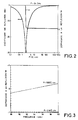
- FIG. 2 represents the variations of the reflection coefficient under normal incidence and of the phase shift at reflection, as a function of the resistivity, for silicon used as photoconductor. It shows that it is possible to pass from a total reflection to an almost total transmission of microwave waves with silicon whose resistivity varies from about 0.1 ohm.cm to more than 1000 ohm.cm depending on its illumination. It also shows that there is a lighting condition for which the silicon completely absorbs the microwave frequencies. This effect can be used to make the antenna absorbent, therefore stealthy for a detection system.
- FIG. 4 gives an example of distribution of the photoconductive elements on the surface of the substrate 20.
- These oversample the mesh of the network of elementary reflectors at the pitch of ⁇ / 2 represented in solid lines, with a mesh four times finer represented in dotted lines .
- each elementary reflector is formed by a paving of 16 photoconductive elements 1a; ..., 4d which it is possible to illuminate individually via the pixels of the liquid crystal screen in order to make them at will. insulators or conductors.
- a horizontal polarization and a vertical polarization see the same phase shift if the photoconductive surface made conductive has a shape preserved in a rotation of ⁇ / 2.
Description
La présente invention concerne une antenne hyperfréquence utilisant, pour le pointage de son faisceau, un réseau de réflecteurs élémentaires à éléments actifs capables de modifier, à volonté, sous le contrôle d'une commande optique, la longueur du trajet de pénétration des ondes hyperfréquences dans les réflecteurs du réseau pour engendrer des déphasages variant d'un réflecteur élémentaire à l'autre et assurer le pointage du faisceau d'antenne.The present invention relates to a microwave antenna using, for the pointing of its beam, a network of elementary reflectors with active elements capable of modifying, at will, under the control of an optical command, the length of the path of penetration of the microwave waves in the network reflectors to generate phase shifts varying from one elementary reflector to another and ensure the pointing of the antenna beam.
Une antenne connue de ce genre possède un réflecteur réalisé à partir d'un substrat en un matériau diélectrique à faibles pertes pour les ondes hyperfréquences, transparent à la lumière, tel que de l'oxyde de silice SiO₂ ou de l'alumine cristallisée AL₂ O₃. Du côté exposé aux hyperfréquences ce substrat est revêtu d'éléments photoconducteurs isolés entre eux par un matériau électriquement isolant, éventuellement recouverts d'une couche opaque transparente aux hyperfréquences, et disposés en réseau avec un pas de maillage égal à λ/2 pour éviter les angles multiples de réflexion, λ étant la longueur d'onde des hyperfréquences considérées. Du côté opposé, non exposé aux hyperfréquences, il est revêtu d'une électrode transparente à la lumière réalisée en un matériau électriquement conducteur tel que de l'oxyde d'étain ITO.A known antenna of this kind has a reflector produced from a substrate made of a dielectric material with low losses for microwave waves, transparent to light, such as silica oxide SiO₂ or crystallized alumina AL₂ O₃ . On the side exposed to microwave frequencies, this substrate is coated with photoconductive elements insulated from one another by an electrically insulating material, possibly covered with an opaque layer transparent to microwave frequencies, and arranged in a network with a mesh pitch equal to λ / 2 to avoid multiple angles of reflection, λ being the wavelength of the microwaves considered. On the opposite side, not exposed to microwave frequencies, it is coated with a light-transparent electrode made of an electrically conductive material such as ITO tin oxide.
Les éléments photoconducteurs, qui peuvent être en silicium "intrinsèque" c'est à dire isolant, sont éclairés ou non sur commande au travers du substrat et de l'électrode transparente, par exemple à l'aide d'un écran à cristaux liquides plaqué contre le substrat sur l'électrode transparente et éclairé par une source lumineuse. Lorsqu'ils sont éclairés, ils deviennent électriquement conducteurs et réfléchissent les ondes hyperfréquences avant qu'elles ne pénètrent dans le substrat. Lorsqu'ils ne sont pas éclairés, ils sont électriquement isolants et se laissent traverser par les ondes hyperfréquences qui pénètrent au travers du substrat et se réfléchissent sur l'électrode transparente. Si le retard de propagation à travers les épaisseurs des éléments photoconducteurs et du substrat est proche d'un nombre impair de quarts de période de l'onde hyperfréquence, le déphasage obtenu entre des ondes hyperfréquences selon qu'elles rencontrent un élément photoconducteur éclairé ou un élément photoconducteur non éclairé est de ¶.The photoconductive elements, which can be made of "intrinsic" silicon, that is to say insulating, are lit or not on command through the substrate and the transparent electrode, for example using a plated liquid crystal screen. against the substrate on the transparent electrode and lit by a light source. When lit, they become electrically conductive and reflect microwave waves before they enter the substrate. When they are not lit, they are electrically insulating and pass through the microwave waves which penetrate through the substrate and are reflected on the transparent electrode. If the propagation delay through the thicknesses of the photoconductive elements and of the substrate is close to an odd number of quarter periods of the microwave wave, the phase shift obtained between microwave waves depending on whether they meet an illuminated photoconductive element or a unlit photoconductive element is ¶.
On réalise ainsi un réseau de réflecteurs élémentaires, avec un maillage au pas de la moitié de la longueur d'onde des hyperfréquences, qui sont capables chacun d'engendrer à volonté des déphasages de 0 ou ¶ sous contrôle d'une commande optique. Cependant, les performances d'une antenne hyperfréquence à balayage concernant le gain, le niveau de lobes secondaires et le diffus nécessitent, en général, pour être acceptables, l'utilisation d'un déphaseur commandable à plus de deux états de phase au niveau de chaque réflecteur élémentaire.One thus realizes a network of elementary reflectors, with a mesh with the step of half of the wavelength of the microwaves, which are each capable of generating at will phase shifts of 0 or ¶ under the control of an optical command. However, the performance of a scanning microwave antenna concerning the gain, the level of secondary lobes and the diffuse generally requires, to be acceptable, the use of a phase shifter controllable with more than two phase states at the level of each elementary reflector.
Pour satisfaire cette exigence, il a été proposé d'empiler des couches de silicium photoconducteur et de substrat diélectrique à faible perte devant l'électrode conductrice transparente pour présenter à l'onde hyperfréquence, au sein de chaque réflecteur élémentaire, différents chemins de longueurs échelonnées qui correspondent à diverses valeurs de déphasage comprises entre 0 et 2¶ et qui sont fonctions de la profondeur dans l'empilement de la première couche de silicium photoconducteur rendue conductrice par éclairement. On rencontre alors des difficultés pour l'illumination sélective des différentes couches de silicium photoconducteur qui se masquent les unes les autres.To meet this requirement, it has been proposed to stack layers of photoconductive silicon and low loss dielectric substrate in front of the transparent conductive electrode in order to present to the microwave wave, within each elementary reflector, different paths of staggered lengths. which correspond to various phase shift values between 0 and 2¶ and which are a function of the depth in the stack of the first photoconductive silicon layer made conductive by illumination. Difficulties are then encountered in the selective illumination of the different photoconductive silicon layers which mask each other.
La présente invention a pour but de remédier à ces difficultés et de permettre l'obtention de déphaseurs commandables à plus de deux états de phase dans un réseau de réflecteurs pour onde hyperfréquence tout en conservant pour le réseau de réflecteurs une structure simple à trois couches formée d'un substrat en matériau diélectrique à faible perte transparent à la lumière portant, du côté exposé aux hyperfréquences, un réseau d'éléments photoconducteurs et, du côté opposé, une électrode conductrice transparente à la lumière.The present invention aims to remedy these difficulties and allow obtaining phase controllers controllable in more than two phase states in a network of reflectors for microwave waves while retaining for the array of reflectors a simple three-layer structure formed of a substrate of dielectric material with low loss transparent to light carrying, on the side exposed to microwave frequencies, an array of photoconductive elements and, on the opposite side, a conductive electrode transparent to the light.
Elle a pour objet une antenne hyperfréquence à balayage optoélectronique pourvue d'une part, d'un réseau de réflecteurs élémentaires à déphaseurs commandés optiquement comportant un substrat en un matériau diélectrique à faibles pertes en hyperfréquences, transparent à la lumière, revêtu, du côté exposé aux hyperfréquences, d'une couche d'éléments photoconducteurs répartis en réseau, et, du côté opposé, d'une électrode conductrice transparente à la lumière, et d'autre part, de moyens d'éclairement sélectif des éléments photoconducteurs aptes à faire passer ces derniers d'un état électriquement isolant à un état conducteur et réciproquement. Cette antenne est remarquable en ce que le réseau d'éléments photoconducteurs présente un maillage qui suréchantillonne le maillage du réseau de réflecteurs élémentaires. Ainsi, chaque réflecteur élémentaire regroupe n² éléments photoconducteurs, n étant le taux de suréchantillonnage, dont une proportion plus ou moins grande est éclairée ce qui lui procure différents états de phase échelonnés depuis une valeur minimale obtenue lorsque tous ses éléments photoconducteurs sont éclairés jusqu'à une valeur maximale obtenue lorsque tous ses éléments photoconducteurs sont dans l'obscurité.It relates to an optoelectronic scanning microwave antenna provided on the one hand with an array of elementary reflectors with optically controlled phase shifters comprising a substrate made of a dielectric material with low microwave losses, transparent to light, coated on the exposed side at microwave frequencies, a layer of photoconductive elements distributed in a network, and, on the opposite side, a conductive electrode transparent to light, and on the other hand, means for selective illumination of the photoconductive elements capable of passing the latter from an electrically insulating state to a conductive state and vice versa. This antenna is remarkable in that the network of photoconductive elements has a mesh which oversamples the mesh of the network of elementary reflectors. Thus, each elementary reflector groups together n² photoconductive elements, n being the oversampling rate, a greater or lesser proportion of which is illuminated, which gives it different phase states staggered from a minimum value obtained when all of its photoconductive elements are lit up to a maximum value obtained when all of its photoconductive elements are in the dark.
D'autres caractéristiques et avantages de l'invention ressortiront de la description d'un mode de réalisation donné à titre d'exemple. Cette description sera faite ci-après, en regard du dessin dans lequel :
- une figure 1 représente, de manière schématique et partiellement démontée, une antenne hyperfréquence à balayage optoélectronique selon l'invention ;
- une figure 2 est un diagramme qui représente les variations du coefficient de réflexion sous incidence normale et du déphasage à la réflexion, en fonction de la résistivité, pour du silicium utilisé comme photoconducteur ;
- une figure 3 est un diagramme qui représente les variations du déphasage à la transmission et à la réflexion du silicium en fonction de la fréquence et
- une figure 4 illustre un exemple de répartition d'éléments photoconducteurs à la surface d'un réflecteur élémentaire de l'antenne représentée à la figure 1.
- Figure 1 shows, schematically and partially disassembled, an optoelectronic scanning microwave antenna according to the invention;
- FIG. 2 is a diagram which represents the variations of the reflection coefficient under normal incidence and phase shift to reflection, as a function of the resistivity, for silicon used as photoconductor;
- FIG. 3 is a diagram which represents the variations of the phase shift during transmission and at reflection of the silicon as a function of the frequency and
- FIG. 4 illustrates an example of distribution of photoconductive elements on the surface of an elementary reflector of the antenna shown in FIG. 1.
L'antenne hyperfréquence représentée à la figure 1 fonctionne aux environs de 94 GHz. Elle comporte un cornet 1 qui illumine avec une onde hyperfréquence un réseau plan 2 de réflecteurs élémentaires placé devant un écran à cristaux liquides 3 éclairé par une source lumineuse 4 au travers d'une optique de focalisation 5.The microwave antenna shown in Figure 1 operates around 94 GHz. It comprises a
Le réseau de réflecteurs élémentaires se présente sous la forme d'un disque plat d'environ 10 cm de diamètre. Il est constitué d'un substrat 20 en un matériau diélectrique à faibles pertes en hyperfréquences, transparent à la lumière, tel que de l'oxyde de Silice Si 0₂ ou de l'alumine cristallisée AL₂ 0₃. Du côté tourné vers le cornet 1, qui est exposé aux hyperfréquences, ce substrat 20 porte une couche 21 d'éléments photoconducteurs tel que du silicium ou de l'arséniure de gallium qui sont isolés entre eux et répartis à la surface du substrat de manière à suréchantillonner le maillage d'un réseau de réflecteurs élémentaires au pas de λ /2 ici, environ 1,5 mm. Du côté opposé au cornet 1, le substrat 20 est revêtu d'une électrode conductrice 22 transparente à la lumière qui est, par exemple, en oxyde d'étain.The network of elementary reflectors is in the form of a flat disc about 10 cm in diameter. It consists of a
L'écran à cristaux liquides 3 est plaqué contre l'électrode conductrice 22 du substrat 20. Il comporte un réseau de pixels qui reproduisent fidèlement la répartition des éléments photoconducteurs 21 portés par le substrat 20 et qui peuvent être rendus, sur commande, soit transparents, soit opaques afin de provoquer, de manière sélective, l'éclairage des éléments photoconducteurs placés dans leur prolongement.The
La source lumineuse 4 peut être un réseau de diodes électroluminescentes ou de lasers fournissant une puissance de 30 à 50 Watts en continu à une longueur d'ondes de 0,8 »m environ. L'intensité lumineuse arrivant sur un élément photoconducteur en silicium, lorsque le pixel de l'écran de cristaux liquides qui lui est associé est transparent, est alors suffisante pour rendre ledit élément conducteur.The
La figure 2 représente les variations du coefficient de réflexion sous incidence normale et du déphasage à la réflexion, en fonction de la résistivité, pour du silicium utilisé comme photoconducteur. Elle montre qu'il est possible de passer d'une réflexion totale à une transmission quasi totale des ondes hyperfréquences avec du silicium dont la résistivité varie de 0,1 ohm.cm environ à plus de 1000 ohm.cm en fonction de son éclairement. Elle montre également qu'il existe une condition d'éclairement pour laquelle le silicium absorbe complétement les hyperfréquences. Cet effet peut être utilisé pour rendre l'antenne absorbante, donc furtive pour un système de détection.FIG. 2 represents the variations of the reflection coefficient under normal incidence and of the phase shift at reflection, as a function of the resistivity, for silicon used as photoconductor. It shows that it is possible to pass from a total reflection to an almost total transmission of microwave waves with silicon whose resistivity varies from about 0.1 ohm.cm to more than 1000 ohm.cm depending on its illumination. It also shows that there is a lighting condition for which the silicon completely absorbs the microwave frequencies. This effect can be used to make the antenna absorbent, therefore stealthy for a detection system.
La figure 3 représente la réponse en fréquence du déphasage à la transmission (P=1000 ohm.cm) et à la réflexion (P=0,18 ohm.cm) du silicium. Elle montre que le déphasage à la transmission est pratiquement nul pour une onde hyperfréquence de 94 GHz.FIG. 3 represents the frequency response of the phase shift to the transmission (P = 1000 ohm.cm) and to the reflection (P = 0.18 ohm.cm) of the silicon. It shows that the phase shift during transmission is practically zero for a 94 GHz microwave wave.
La figure 4 donne un exemple de répartition des éléments photoconducteurs à la surface du substrat 20. Ceux-ci suréchantillonnent le maillage du réseau de réflecteurs élémentaires au pas de λ/2 représenté en traits pleins, avec un maillage quatre fois plus fin représenté en pointillés. Ainsi, chaque réflecteur élémentaire est formé d'un dallage de 16 éléments photoconducteurs 1a;...,4d qu'il est possible d'éclairer individuellement par l'intermédiaire des pixels de l'écran à cristaux liquides afin de les rendre à volonté isolants ou conducteurs. On peut alors choisir une forme variable de la surface photoconductrice éclairée dans chaque réflecteur élémentaire pour définir une phase variable. Cela revient à l'introduction, dans un guide d'onde hyperfréquence matérialisé par le contour d'un réflecteur élémentaire, d'un iris conducteur qui est équivalent à une susceptance dont on sait calculer la phase en réflexion. Cette susceptance variable peut être la même pour plusieurs polarisations hyperfréquences si celles-ci voient des surfaces équivalentes.FIG. 4 gives an example of distribution of the photoconductive elements on the surface of the
Par exemple, une polarisation horizontale et une polarisation verticale voient le même déphasage si la surface de photoconducteur rendue conductrice a une forme conservée dans une rotation de ¶/2.For example, a horizontal polarization and a vertical polarization see the same phase shift if the photoconductive surface made conductive has a shape preserved in a rotation of ¶ / 2.
Dans le cas illustré par la figure 4 où un réflecteur élémentaire est constitué d'un dallage de 16 éléments photoconducteurs 1a,...,4d on peut adopter cinq configurations différentes conservées par une rotation de ¶/2 :
- une première configuration où aucun élément photoconducteur n'est éclairé ;
- une deuxième configuration, qui est celle représentée, où seuls les éléments photoconducteurs en coin 1a, 4a, 4d et 1d sont éclairés ;
- une troisième configuration où les éléments photoconducteurs 2a, 4b, 3d et 1c sont éclairés en plus des éléments photoconducteurs en coin 1a, 4a, 4d, et 1d ;
- une quatrième configuration où tous les éléments photoconducteurs du pourtour 1a, 2a, 3a, 4a, 4b, 4d, 3d, 2d, 1d, 1c, et 1b sont éclairés ;
- une cinquième configuration où tous les éléments photoconducteurs sont éclairés.
- a first configuration where no photoconductive element is lit;
- a second configuration, which is that shown, where only the corner photoconductive elements 1a, 4a, 4d and 1d are lit;
- a third configuration where the photoconductive elements 2a, 4b, 3d and 1c are lit in addition to the corner photoconductive elements 1a, 4a, 4d, and 1d;
- a fourth configuration where all the photoconductive elements of the periphery 1a, 2a, 3a, 4a, 4b, 4d, 3d, 2d, 1d, 1c, and 1b are lit;
- a fifth configuration where all the photoconductive elements are illuminated.
Si les épaisseurs des éléments photoconducteurs et du substrat sont de l'ordre de la moitié de la longueur d'onde des hyperfréquences utilisées on obtient avec les quatre dernières configurations un déphaseur commandé à deux bits indépendant de la polarisation.If the thicknesses of the photoconductive elements and of the substrate are of the order of half of the wavelength of the microwaves used, a two-bit controlled phase shifter independent of the polarization is obtained with the last four configurations.
Bien évidemment, on peut adopter un taux de suréchantillonnage moindre par exemple de deux ou trois mais on a alors un moindre choix de configurations ou supérieur mais on se heurte alors à des difficultés de réalisation dues à la petitesse des éléments photoconducteurs et des pixels de l'écran à cristaux liquides qui doivent leur correspondre.Obviously, we can adopt a lower oversampling rate, for example two or three, but we then has a lesser choice of configurations or higher but we then come up against production difficulties due to the smallness of the photoconductive elements and of the pixels of the liquid crystal screen which must correspond to them.
Claims (3)
- Optoelectronic scanning microwave antenna provided, on the one hand, with an array (2) of optically-controlled elementary reflectors comprising a substrate (20) made of a dielectric material having low loss at microwave frequencies and being transparent to light, the said substrate being coated, on the side exposed to the microwaves, with a layer (21) of photoconductive elements distributed in an array and, on the opposite side, with a conductive electrode (22) transparent to light and, on the other hand, with means (3, 4, 5) for selective illumination of the photoconductive elements, capable of making these elements pass from an electrically insulating state to a conductive state and vice versa, characterized in that the array of photoconductive elements forms a lattice which subdivides the lattice of the array of elementary reflectors.
- Antenna according to Claim 1, characterized in that the array of photoconductive elements forms a lattice which subdivides the lattice of the array of elementary reflectors by a subdivision factor equal to four, each elementary reflector containing a tiling arrangement of sixteen photoconductive elements.
- Antenna according to Claim 1, characterized in that the photoconductive elements belonging to an elementary reflector are illuminated selectively so as to form configurations of conductive elements and electrically insulating elements which are invariant under rotations π/2.
Applications Claiming Priority (2)
| Application Number | Priority Date | Filing Date | Title |
|---|---|---|---|
| FR9107422A FR2678112B1 (en) | 1991-06-18 | 1991-06-18 | MICROWAVE ANTENNA WITH OPTOELECTRONIC SCANNING. |
| FR9107422 | 1991-06-18 |
Publications (2)
| Publication Number | Publication Date |
|---|---|
| EP0519772A1 EP0519772A1 (en) | 1992-12-23 |
| EP0519772B1 true EP0519772B1 (en) | 1995-06-21 |
Family
ID=9413948
Family Applications (1)
| Application Number | Title | Priority Date | Filing Date |
|---|---|---|---|
| EP92401383A Expired - Lifetime EP0519772B1 (en) | 1991-06-18 | 1992-05-21 | Microwave antenna with optoelectronical controlled scanning |
Country Status (4)
| Country | Link |
|---|---|
| US (1) | US5262796A (en) |
| EP (1) | EP0519772B1 (en) |
| DE (1) | DE69203044T2 (en) |
| FR (1) | FR2678112B1 (en) |
Families Citing this family (13)
| Publication number | Priority date | Publication date | Assignee | Title |
|---|---|---|---|---|
| NL9400863A (en) * | 1994-05-26 | 1996-01-02 | Hollandse Signaalapparaten Bv | Adjustable microwave antenna |
| EP0680111B1 (en) * | 1994-04-29 | 2001-11-21 | Thales Nederland B.V. | Adjustable microwave antenna |
| FR2763746B1 (en) | 1997-05-23 | 1999-07-30 | Thomson Csf | METHOD AND DEVICE FOR CONNECTING TWO MILLIMETER ELEMENTS |
| FR2769130B1 (en) | 1997-09-30 | 2001-06-08 | Thomson Csf | METHOD FOR COATING AN ELECTRONIC CHIP AND ELECTRONIC CARD COMPRISING AT LEAST ONE COATED CHIP ACCORDING TO THIS PROCESS |
| US6091371A (en) * | 1997-10-03 | 2000-07-18 | Motorola, Inc. | Electronic scanning reflector antenna and method for using same |
| US6232931B1 (en) | 1999-02-19 | 2001-05-15 | The United States Of America As Represented By The Secretary Of The Navy | Opto-electronically controlled frequency selective surface |
| US6597327B2 (en) * | 2000-09-15 | 2003-07-22 | Sarnoff Corporation | Reconfigurable adaptive wideband antenna |
| US6621459B2 (en) | 2001-02-02 | 2003-09-16 | Raytheon Company | Plasma controlled antenna |
| GB0323123D0 (en) * | 2003-10-03 | 2003-11-05 | Roke Manor Research | Electronically steerable fresnel zone antenna |
| GB0706301D0 (en) * | 2007-03-30 | 2007-05-09 | E2V Tech Uk Ltd | Reflective means |
| US8044866B2 (en) * | 2007-11-06 | 2011-10-25 | The Boeing Company | Optically reconfigurable radio frequency antennas |
| US9595757B2 (en) * | 2013-12-24 | 2017-03-14 | The Boeing Company | Integral RF-optical phased array module |
| US9966647B1 (en) * | 2016-06-20 | 2018-05-08 | The United States Of America, As Represented By The Secretary Of The Navy | Optically defined antenna |
Family Cites Families (15)
| Publication number | Priority date | Publication date | Assignee | Title |
|---|---|---|---|---|
| FR2264434B1 (en) * | 1974-03-12 | 1976-07-16 | Thomson Csf | |
| FR2346897A1 (en) * | 1975-01-22 | 1977-10-28 | Thomson Csf | HYPERFREQUENCY MILLIMETRIC CIRCUIT |
| FR2346854A1 (en) * | 1975-10-02 | 1977-10-28 | Thomson Csf | INTEGRATED CIRCUIT INCLUDING A SOURCE OF MILLIMETRIC WAVES, AND METHOD OF MANUFACTURING THE SAID CIRCUIT |
| FR2351503A1 (en) * | 1976-05-11 | 1977-12-09 | Thomson Csf | PROCESS FOR MAKING A CIRCUIT FOR MILLIMETRIC WAVES INCLUDING A SEMICONDUCTOR DIODE AND ANOTHER SEMICONDUCTOR COMPONENT, AND DEVICES MADE BY THIS PROCEDURE |
| FR2368151A1 (en) * | 1976-10-15 | 1978-05-12 | Thomson Csf | SOLID STATE MILLIMETRIC WAVES SOURCE WITH AN INTEGRATED DIRECTIVE AERIAL |
| FR2421478A2 (en) * | 1978-03-31 | 1979-10-26 | Thomson Csf | SOLID STATE MILLIMETRIC WAVE SOURCE CONTAINING A DIRECTIVE AERIAL |
| FR2423088A1 (en) * | 1978-04-14 | 1979-11-09 | Thomson Csf | MILLIMETRIC WAVE SOURCE INCLUDING AN OSCILLATOR MODULE AND A VARIABLE CAPACITY TUNING MODULE, AND EMITTER INCLUDING SUCH SOURCE |
| FR2452201A1 (en) * | 1979-03-23 | 1980-10-17 | Thomson Csf | SYMMETRIC MIXER FOR MILLIMETER WAVES AND RECEIVER USING SUCH A MIXER |
| FR2458819A1 (en) * | 1979-06-12 | 1981-01-02 | Thomson Csf | SIMULTANEOUS EMISSION AND RECEPTION HEAD, MILLIMETER WAVE EMITTER-RECEIVER AND RADAR USING SUCH HEAD |
| US4479131A (en) * | 1980-09-25 | 1984-10-23 | Hughes Aircraft Company | Thermal protective shield for antenna reflectors |
| JP2508707B2 (en) * | 1987-04-28 | 1996-06-19 | 三菱電機株式会社 | Light control antenna device |
| FR2628893B1 (en) * | 1988-03-18 | 1990-03-23 | Thomson Csf | MICROWAVE SWITCH |
| GB2225122B (en) * | 1988-11-09 | 1992-12-23 | Emi Plc Thorn | An apparatus for producing a phase shift in a beam of electromagnetic radiation |
| US5014069A (en) * | 1989-09-15 | 1991-05-07 | The United States Of America As Represented By The Secretary Of The Air Force | Photoconductive antenna modulator |
| NL9000369A (en) * | 1990-02-16 | 1991-09-16 | Hollandse Signaalapparaten Bv | ANTENNA SYSTEM WITH VARIABLE BUNDLE WIDTH AND BUNDLE ORIENTATION. |
-
1991
- 1991-06-18 FR FR9107422A patent/FR2678112B1/en not_active Expired - Fee Related
-
1992
- 1992-05-21 EP EP92401383A patent/EP0519772B1/en not_active Expired - Lifetime
- 1992-05-21 DE DE69203044T patent/DE69203044T2/en not_active Expired - Fee Related
- 1992-06-12 US US07/897,776 patent/US5262796A/en not_active Expired - Lifetime
Also Published As
| Publication number | Publication date |
|---|---|
| DE69203044D1 (en) | 1995-07-27 |
| EP0519772A1 (en) | 1992-12-23 |
| FR2678112A1 (en) | 1992-12-24 |
| DE69203044T2 (en) | 1995-11-02 |
| FR2678112B1 (en) | 1993-12-03 |
| US5262796A (en) | 1993-11-16 |
Similar Documents
| Publication | Publication Date | Title |
|---|---|---|
| EP0519772B1 (en) | Microwave antenna with optoelectronical controlled scanning | |
| EP0539297B1 (en) | Device with adjustable frequency selective surface | |
| EP0667984B1 (en) | Monopolar wire-plate antenna | |
| CA2074657C (en) | Microwave antenna array | |
| EP0145597A2 (en) | Plane periodic antenna | |
| EP0206846B1 (en) | Microwave phase shifter, especially in the millimeter wave range, with a piezoelectric control | |
| CA2460820C (en) | Broadband or multiband antenna | |
| EP0548876B1 (en) | An active offset antenna having two reflectors | |
| WO2001039325A1 (en) | Active electronic scan microwave reflector | |
| FR2656468A1 (en) | MAGIC MICROWAVE RADIATION SOURCE AND ITS APPLICATION TO AN ELECTRONIC SCAN ANTENNA. | |
| FR2512280A1 (en) | Solid state microwave antenna sweep reflector - has number of addressable diodes in matrix selectively switched to form transparent or reflective panel | |
| EP1305846A1 (en) | Active dual-polarization microwave reflector, in particular for electronically scanning antenna | |
| EP0595726A1 (en) | Phase shifter for electromagnetic waves and application in an antenna with electronic scanning | |
| FR2685550A1 (en) | HYPERFREQUENCY REFLECTIVE ELEMENT. | |
| CA2023210C (en) | Spiral-antennae system | |
| WO1991018428A1 (en) | Planar orientable antenna operating in the microwave band | |
| EP1157444B1 (en) | Antenna with double-band electronic scanning, with active microwave reflector | |
| EP0762534B1 (en) | Method for enlarging the radiation diagram of an antenna array with elements distributed in a volume | |
| EP0524878A1 (en) | Microwave semiconductor absorber with optical command | |
| FR2747842A1 (en) | Microwave lens with panel of stacked phase shifting channels | |
| EP0088681B1 (en) | Dual-reflector antenna with incorporated polarizer | |
| EP4189772A1 (en) | Metasurface device | |
| EP1133000B1 (en) | Active microwave reflector for antenna with electronic scanning | |
| FR2689320A1 (en) | Radar aerial comprising reflective elements using electronic scanning - has array of reflectors, each comprising set of interlinked orthogonal bars | |
| FR2677493A1 (en) | NETWORK OF RADIANT ELEMENTS WITH AUTOCOMPLEMENTARY TOPOLOGY, AND ANTENNA USING SUCH A NETWORK. |
Legal Events
| Date | Code | Title | Description |
|---|---|---|---|
| PUAI | Public reference made under article 153(3) epc to a published international application that has entered the european phase |
Free format text: ORIGINAL CODE: 0009012 |
|
| AK | Designated contracting states |
Kind code of ref document: A1 Designated state(s): DE FR GB IT SE |
|
| 17P | Request for examination filed |
Effective date: 19930113 |
|
| K1C3 | Correction of patent application (complete document) published |
Effective date: 19921223 |
|
| RAP1 | Party data changed (applicant data changed or rights of an application transferred) |
Owner name: THOMSON-CSF |
|
| 17Q | First examination report despatched |
Effective date: 19941107 |
|
| GRAA | (expected) grant |
Free format text: ORIGINAL CODE: 0009210 |
|
| AK | Designated contracting states |
Kind code of ref document: B1 Designated state(s): DE FR GB IT SE |
|
| ITF | It: translation for a ep patent filed |
Owner name: JACOBACCI & PERANI S.P.A. |
|
| REF | Corresponds to: |
Ref document number: 69203044 Country of ref document: DE Date of ref document: 19950727 |
|
| GBT | Gb: translation of ep patent filed (gb section 77(6)(a)/1977) |
Effective date: 19950713 |
|
| PLBE | No opposition filed within time limit |
Free format text: ORIGINAL CODE: 0009261 |
|
| STAA | Information on the status of an ep patent application or granted ep patent |
Free format text: STATUS: NO OPPOSITION FILED WITHIN TIME LIMIT |
|
| 26N | No opposition filed | ||
| REG | Reference to a national code |
Ref country code: GB Ref legal event code: IF02 |
|
| REG | Reference to a national code |
Ref country code: FR Ref legal event code: CD |
|
| PGFP | Annual fee paid to national office [announced via postgrant information from national office to epo] |
Ref country code: SE Payment date: 20030507 Year of fee payment: 12 |
|
| PGFP | Annual fee paid to national office [announced via postgrant information from national office to epo] |
Ref country code: FR Payment date: 20030508 Year of fee payment: 12 |
|
| PGFP | Annual fee paid to national office [announced via postgrant information from national office to epo] |
Ref country code: GB Payment date: 20030519 Year of fee payment: 12 |
|
| PGFP | Annual fee paid to national office [announced via postgrant information from national office to epo] |
Ref country code: DE Payment date: 20030529 Year of fee payment: 12 |
|
| PG25 | Lapsed in a contracting state [announced via postgrant information from national office to epo] |
Ref country code: GB Free format text: LAPSE BECAUSE OF NON-PAYMENT OF DUE FEES Effective date: 20040521 |
|
| PG25 | Lapsed in a contracting state [announced via postgrant information from national office to epo] |
Ref country code: SE Free format text: LAPSE BECAUSE OF NON-PAYMENT OF DUE FEES Effective date: 20040522 |
|
| PG25 | Lapsed in a contracting state [announced via postgrant information from national office to epo] |
Ref country code: DE Free format text: LAPSE BECAUSE OF NON-PAYMENT OF DUE FEES Effective date: 20041201 |
|
| EUG | Se: european patent has lapsed | ||
| GBPC | Gb: european patent ceased through non-payment of renewal fee |
Effective date: 20040521 |
|
| PG25 | Lapsed in a contracting state [announced via postgrant information from national office to epo] |
Ref country code: FR Free format text: LAPSE BECAUSE OF NON-PAYMENT OF DUE FEES Effective date: 20050131 |
|
| REG | Reference to a national code |
Ref country code: FR Ref legal event code: ST |
|
| PG25 | Lapsed in a contracting state [announced via postgrant information from national office to epo] |
Ref country code: IT Free format text: LAPSE BECAUSE OF NON-PAYMENT OF DUE FEES Effective date: 20050521 |