EP0519623B1 - Système de palpeur avec surfaces multiples pour ondes amorties - Google Patents
Système de palpeur avec surfaces multiples pour ondes amorties Download PDFInfo
- Publication number
- EP0519623B1 EP0519623B1 EP92305122A EP92305122A EP0519623B1 EP 0519623 B1 EP0519623 B1 EP 0519623B1 EP 92305122 A EP92305122 A EP 92305122A EP 92305122 A EP92305122 A EP 92305122A EP 0519623 B1 EP0519623 B1 EP 0519623B1
- Authority
- EP
- European Patent Office
- Prior art keywords
- sensor
- waveguide
- radiation
- analyte
- reactant coating
- Prior art date
- Legal status (The legal status is an assumption and is not a legal conclusion. Google has not performed a legal analysis and makes no representation as to the accuracy of the status listed.)
- Expired - Lifetime
Links
Images


Classifications
-
- G—PHYSICS
- G01—MEASURING; TESTING
- G01N—INVESTIGATING OR ANALYSING MATERIALS BY DETERMINING THEIR CHEMICAL OR PHYSICAL PROPERTIES
- G01N21/00—Investigating or analysing materials by the use of optical means, i.e. using sub-millimetre waves, infrared, visible or ultraviolet light
- G01N21/75—Systems in which material is subjected to a chemical reaction, the progress or the result of the reaction being investigated
- G01N21/77—Systems in which material is subjected to a chemical reaction, the progress or the result of the reaction being investigated by observing the effect on a chemical indicator
- G01N21/7703—Systems in which material is subjected to a chemical reaction, the progress or the result of the reaction being investigated by observing the effect on a chemical indicator using reagent-clad optical fibres or optical waveguides
-
- G—PHYSICS
- G01—MEASURING; TESTING
- G01N—INVESTIGATING OR ANALYSING MATERIALS BY DETERMINING THEIR CHEMICAL OR PHYSICAL PROPERTIES
- G01N21/00—Investigating or analysing materials by the use of optical means, i.e. using sub-millimetre waves, infrared, visible or ultraviolet light
- G01N21/62—Systems in which the material investigated is excited whereby it emits light or causes a change in wavelength of the incident light
- G01N21/63—Systems in which the material investigated is excited whereby it emits light or causes a change in wavelength of the incident light optically excited
- G01N21/64—Fluorescence; Phosphorescence
- G01N21/645—Specially adapted constructive features of fluorimeters
- G01N21/648—Specially adapted constructive features of fluorimeters using evanescent coupling or surface plasmon coupling for the excitation of fluorescence
-
- Y—GENERAL TAGGING OF NEW TECHNOLOGICAL DEVELOPMENTS; GENERAL TAGGING OF CROSS-SECTIONAL TECHNOLOGIES SPANNING OVER SEVERAL SECTIONS OF THE IPC; TECHNICAL SUBJECTS COVERED BY FORMER USPC CROSS-REFERENCE ART COLLECTIONS [XRACs] AND DIGESTS
- Y10—TECHNICAL SUBJECTS COVERED BY FORMER USPC
- Y10S—TECHNICAL SUBJECTS COVERED BY FORMER USPC CROSS-REFERENCE ART COLLECTIONS [XRACs] AND DIGESTS
- Y10S435/00—Chemistry: molecular biology and microbiology
- Y10S435/808—Optical sensing apparatus
-
- Y—GENERAL TAGGING OF NEW TECHNOLOGICAL DEVELOPMENTS; GENERAL TAGGING OF CROSS-SECTIONAL TECHNOLOGIES SPANNING OVER SEVERAL SECTIONS OF THE IPC; TECHNICAL SUBJECTS COVERED BY FORMER USPC CROSS-REFERENCE ART COLLECTIONS [XRACs] AND DIGESTS
- Y10—TECHNICAL SUBJECTS COVERED BY FORMER USPC
- Y10S—TECHNICAL SUBJECTS COVERED BY FORMER USPC CROSS-REFERENCE ART COLLECTIONS [XRACs] AND DIGESTS
- Y10S436/00—Chemistry: analytical and immunological testing
- Y10S436/805—Optical property
-
- Y—GENERAL TAGGING OF NEW TECHNOLOGICAL DEVELOPMENTS; GENERAL TAGGING OF CROSS-SECTIONAL TECHNOLOGIES SPANNING OVER SEVERAL SECTIONS OF THE IPC; TECHNICAL SUBJECTS COVERED BY FORMER USPC CROSS-REFERENCE ART COLLECTIONS [XRACs] AND DIGESTS
- Y10—TECHNICAL SUBJECTS COVERED BY FORMER USPC
- Y10S—TECHNICAL SUBJECTS COVERED BY FORMER USPC CROSS-REFERENCE ART COLLECTIONS [XRACs] AND DIGESTS
- Y10S436/00—Chemistry: analytical and immunological testing
- Y10S436/807—Apparatus included in process claim, e.g. physical support structures
Definitions
- This invention relates to improved evanescent wave sensors for use in spectrophotometric signal responsive processing assays of analytes in fluids, and more particularly to such sensors having at least two optical surfaces which carry one or more fluoromeres and/or a reactive coating.
- the evanescent wave is an electromagnetic waveform which typically extends less than a wavelength into the surrounding medium. However, this penetration is sufficient to permit substantial optical interaction between the evanescent wave component and one or more target substances in the medium.
- optical waveguides in the form of fiber optic rods typically are coated with either an antibody or an antigen which binds the corresponding antigen or antibody, respectively, suspected of being present in a medium or test sample. This coating typically is applied prior to the performance of an immunoassay measurement.
- an antibody is bound to the surface of the fiber optic rod to form a reactant coating, and the device is subsequently immersed in a sample suspected of containing the antigen to be analyzed. Antigen present in the sample binds with the attached antibody.
- a second antibody previously labelled by a fluorescent tag, is added to the sample.
- the second, labelled antibody is first mixed with the antigen in the sample, and the mixture is brought into contact with the fiber optic rod and the first, bound antibody.
- the labelled antibody attaches to the antigen to form a tagged complex bound to the fiber optic rod by the first antibody.
- Light is subsequently introduced into the fiber optic rod at one or more wavelengths and is propagated along the fiber optic rod by total internal reflection.
- the reflection is, of course, not completely total since the fluorescent tag absorbs a small amount of the radiation.
- the attached fluorescent tag (referred to as a fluorophore) absorbs energy from the evanescent wave electromagnetic fields at a first wavelength and fluoresces at a second, longer wavelength. Fluorescence from the excited fluorophore passes into the optical waveguide via a tunneling effect and the portion of the fluorescent radiation which occurs at an angle greater than the critical angle is propagated through the optical waveguide to emerge from an output end.
- the waveguide has an elongated rod-shaped core having an opening within the core material.
- a reactant coating is disposed about the opening within the core on a single optical surface.
- an evanescent wave sensor comprising:
- the evanescent wave sensor of the invention has a waveguide with at least two optical surfaces. Radiation is propagated along the waveguide between the first and second surfaces by total internal reflection. The first surface receives a radiation signal which indicates the presence of a first analyte in a medium and the second surface receives a radiation signal representing one or both of a second analyte and/or a reference.
- the sequence and number of radiation signals may vary depending on the type of analyses being performed by the sensor and the fluorescent tags employed with the assay.
- the sensor therefore is capable of detecting one or more analytes in a single medium, detecting simultaneously one or more analytes in two different media, or detecting simultaneously an analyte and a reference. Use of a reference provides an automatic indication of fluctuations in light intensity, defects in the optical surface of the sensor, or other factors which affect the apparent quantity of detected output radiation.
- the waveguide is a hollow core having an inner surface and an outer surface.
- One of the inner and outer surfaces forms the first wave propagating surface and the other of the inner and outer surfaces forms the second wave propagating surface.
- the waveguide is a shell having a radiation port at a first end and a base at a second end, and having inner and outer wall surfaces extending between the radiation port and the base to form the first and second wave propagating surfaces.
- One or both of the first and second surfaces can carry a reactant coating which may include a binding partner of an analyte to be detected.
- the reactant coating may include an immobilized antibody, antigen, enzyme, nucleic acid, receptor, or other known binding molecules.
- the waveguide is transmissive to light which can excite fluorescence of fluorescent tag and is transmissive to fluorescent radiation from the fluorescent tag.
- the sensor may further include a substance or element for isolating the first and second surfaces to prevent contact of a single medium with both surfaces.
- a gel or a solid substance such as polytetrafluoroethylene-co-hexafluoropropylene can be disposed about the second surface to prevent the medium containing the first analyte from contacting the second wave propagating surface. Therefore, a sensor according to the invention is useful for detecting one or more components of a first medium, or one or more components from a second medium.
- the invention further provides a method of assaying at least one anlyte in at least one medium, comprising:
- This method of assaying analytes involves providing an optical waveguide having at least first and second wave propagating surfaces, and contacting the waveguide in the medium to contact at least one of the first and second surfaces. Radiation then is propagated through the waveguide between the first and second surfaces to generate evanescent wave electromagnetic fields at both the first and second surfaces to irradiate the medium, and radiation reentering the waveguide and emitted from it, and is detected to assay the analyte.
- the radiation can interact with an analyte by absorption or by generation of fluorescent radiation.
- Another object of the invention is to provide a sensor having at least two optically independent surfaces which can be illuminated by one or more light input signals.
- Yet another object of the invention is to provide such a sensor which enables two independent assays to be conducted using a single waveguide.
- a still further object of the invention is to provide such a sensor which can enable comparison of a reference output signal with an analyte output signal to determine fluctuations in light intensity or loss due to surface defects.
- Yet another object of the invention is to provide such a sensor which enables a greater acceptable variation of sensor geometry by providing automatic referencing within the waveguide.
- Yet another object of the invention is to provide a sensor which can provide a reference of excitation radiation without contacting the sample with the reference material.
- a still further object of the invention is to provide an improved device for guiding excitation radiation into a sensor according to the invention, and for collecting output radiation.
- a sensor according to the present invention and method for using the sensor can be accomplished by a waveguide having at least two wave propagating surfaces.
- the sensor receives a radiation input signal and emits one or more output signals to detect one or more analytes in at least one medium.
- Analyte shall be understood to include any of a variety of chemical and biochemical substances.
- the analyte sources may include physiological, scientific and industrial (toxic and nontoxic) test media where the presence, absence or quantity of the analyte in the test medium is sought; and where, for example, the analysis of a physiological analyte is relevant to diagnosis and/or treatment of disease.
- the input signal is propagated along the waveguide between the first and second wave propagating surfaces.
- the first surface is capable of receiving a first radiation signal which indicates the presence of a first analyte
- the second surface is capable of receiving a second radiation signal which represents one or both of a second analyte and a reference.
- a reactant coating may be disposed on one or both surfaces.
- a reactant coating as used herein shall be understood to include the attachment by coating means of a molecule which is receptive to a complimentary molecule in a test medium or test sample to form a complex. Coating as used herein shall be understood to include specific and nonspecific reactions including noncovalent binding and covalent binding.
- the evanescent wave electromagnetic fields generated at the first and second surfaces interact with different substances at the two interfaces between the waveguide and a surrounding medium (gas, liquid or solid).
- the first wave propagating surface is coated with a binding partner of a first analyte and the second surface is coated with a reference fluorophore.
- the reactant coating on the first surface binds the first analyte which in turn binds a homologous binding partner carrying a fluorescent tag.
- the reference fluorophore and the fluorescent tag can be selected so that both are excited by a single excitation wavelength and yet each emits at a different wavelength.
- the two different emitted fluorescent radiation wavelengths reenter the waveguide and are detected independently to enable accurate determination of the presence or quantity of the first analyte.
- This configuration and a number of alternative configurations are described in more detail below. Use of the waveguide sensor to analyze more than one media is also described.
- an evanescent wave sensor to provide two or more wave propagating surfaces.
- One configuration involves a planar plate such as a microscope slide.
- Another configuration is a hollow core such as described in U.S. Patent No. 4,880,752, incorporated herein by reference.
- the sensor is a shell having a radiation port at a first end and a base at a second end, with the first and second surfaces extending between the radiation port and the base as described in the above mentioned co-pending European patent application entitled "Evanescent Wave Sensor Shell and Apparatus".
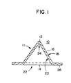
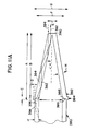
- One construction of a frustoconical shell is shown as sensor 10, Fig. 1.
- sensor 10 includes a shell or cone 11, having a planar radiation port 12 and a base 14.
- a wall 16 extends between the radiation port 12 and the base 14 and defines outer wall surface 18 which forms the first wave propagating surface and inner wall surface 20 which forms the second wave propagating surface.
- the interior of the shell 11 is hollow and the base 14 defines a circular opening 22 which communicates with the interior.
- the inner wall 20 converges to a point 24 beneath the radiation port 12 so that virtually all radiation entering through radiation port 12 impinges at a desired angle on inner wall surface 20.
- the senor 10 further includes handle 26 which is an annular flange connected to the base 14.
- handle 26 is a non-active surface, and therefore can be grasped without damaging an optically active surface.
- the radiation port 12 and wall surfaces 18 and 20 are optically active surfaces which are optically polished. Both incoming excitation radiation and outgoing fluorescent radiation, of fluorescent compounds known in the art, reflect off the optically polished surfaces 18 and 20 without effect by the handle 26. Radiation which exits through the base 14 or the handle 26 will not affect the assay.
- the handle is integral, it need not be integral but can be a separate member attached to the sensor.
- the lower portion of the shell 11 can be designed as a handle and not used as an optically active area.
- One technique or mechanism for holding a sensor without interfering with the optically active area is disclosed in U.S. Patent No. 4,671,938 (Cook et al), incorporated herein by reference.
- the dimensions of the preferred waveguide sensor 10 are as follows.
- the radiation port 12 has an outer diameter of 0.92 mm, and the base 14 has an outer diameter of 10.26 mm.
- the handle 26 has an outer diameter of 16 mm which provides nearly 5 mm of graspable surface along all sides of the shell 11.
- the sensor 10 is approximately 11.5 mm in length, including a thickness of 0.5 mm for the handle 26.
- the wall 16 also has a uniform wall thickness of 0.5 mm to provide a large number of internal reflections along its,length.
- the material is polymethyl methacrylate (PMMA) having an index of refraction of 1.4917 at a wavelength of 589.3 nm.
- PMMA polymethyl methacrylate
- the sensor 10 in comparison to fiber optic rods as used in the art, has a large surface area for its length.
- the outer wall surface 18 has an area of approximately 170 mm 2 . This area is slightly greater than the 157 mm 2 of a 50 mm fiber optic rod having a diameter of 1 mm as is presently used in fluorescent immunoassays.
- the material is injection moldable so that the sensor may be rapidly and inexpensively formed, and easily mass produced. Further, optically polishing the mold establishes optically polished surfaces which do not require further polishing. Another factor is that the material must have an index of refraction greater than that of the intended medium to be analyzed, as described below. Additionally, it is desirable for the material to be optically pure and provide low attenuation of the radiation of interest.
- Silica glass is suitable for ultraviolet or visible radiation
- plastics such as polymethylmethacrylate (PMMA), polystyrene, and polycarbonate are suitable for visible radiation
- fluoride glass or chalcogenide are suitable for near infrared radiation.
- Other organic polymeric materials such as silicones, acrylates, fluoroacrylates, and the like can also be used as the sensor material. It is also desirable for the material to be nonfluorescent to the radiation of interest for assays involving fluorescence.
- the material it is desirable for the material to have suitable surface properties for binding of a reactant coating to it, or to be amendable to modification to assist bonding.
- PMMA is preferred not only for its optical purity and its injection molding characteristics, but also because it is hydrophobic which enables antibodies and other proteins to be attached to the surface simply by bringing them in contact with the PMMA.
- a silane coating it is desirable to add a silane coating to provide either a hydrophobic surface or one amendable to covalent coupling chemistries.
- the shell 10 has an angle a as shown in Fig. 2A.
- the angle a represents the inclination of the axis of propagation 32 relative to the cone axis 30 which passes through the center of the radiation port 12 and the base 14.
- the axis of propagation 32 passes through the center of wall 16, halfway between outer wall surface 18 and inner wall surface 20 which are parallel to each other relative to the angle of propagation.
- the inclination of outer and inner wall surfaces 18, 20 and the cone axis 30 is also angle a.
- Light ray 34 is shown propagating through the wall 16 after passing through the port 12, and bouncing between inner wall surface 20 and other wall surface 18 due to total internal reflection.
- Total internal reflection occurs when the angle of the ray 34 is greater than the critical angle, which in turn depends upon the index of refraction n 1 of the wall 16 relative to the index of refraction n 2 of a first medium, typically air, through which radiation passes to enter and exit the radiation port 12, and the index of refraction n 3 of a second medium, typically a liquid L, which surrounds a lower portion of the sensor 10 and contacts only the outer surface 18 as illustrated, or contacts both outer surface 18 and inner surface 20 as described below.
- air surrounds the remainder of the shell 11 including radiation port 12 and all of the inner wall surface 20.
- the liquid L is contacted to a portion of the outer wall 18, which is coated with a reactant coating 36 which may be an immobilized antibody, an antigen, a receptor, a nucleic acid, an enzyme, or other binding substances as is known in the art. It is desirable for the reactant coating to bind an analyte suspected of being present in the medium.
- the inner wall surface 20 is coated with a reference fluorophore 37 such as a binding substance labelled with a fluorescent dye.
- a first antibody is attached or coated to the outer surface 18 and a reference fluorophore is attached to the inner surface 20 by separate dip-coating steps after the surfaces 18, 20 are suitably cleaned.
- One technique for cleaning the surfaces 18, 20 is by sonicating the sensor for several seconds while it is immersed in a Freon TF bath.
- the first antibody attached to the outer surface 18, forms a complex when a first analyte in the liquid L contacts the first antibody.
- a typical antibody has a height of approximately 100 angstroms (A), and binds an antigen having a typical thickness of 100-200 A in the case of a large molecular weight antigen.
- a second, antibody having an attached fluorophore is then contacted against the antigen to form a tagged complex having a fluorophore spaced approximately 300-400 A from the outer wall surface 18.
- an evanescent wave excites the fluorophore which induces emission at a longer wavelength.
- the fluorescent emission is indicated by rays 40, shown in phantom.
- the portion of the rays 40 which are internally reflected are propagated back through the radiation port 12 and detected as described below. This portion depends strongly on he distance of the fluorophore from the PMMA/media interface, and decreases rapidly with increasing distance as expected for a tunneling-like effect.
- an evanescent wave excites the reference fluorophore 37 which induces emission at a different wavelength, as indicated by rays 41, shown in phantom. Both fluorescent radiation 40 from the reactant coating 36 and the fluorescent radiation 41 from the reference fluorophore 37 are shown exiting from the radiation port 12 for subsequent detection.
- the parameters of a particular cone construction are as follows.
- n 3 of the second medium the sample to be analyzed
- n 3 is used as described below.
- the reference fluorophore 37 is sufficiently thin so that it does not significantly alter the index of refraction of the surrounding air.
- a plastic material such as PMMA has an index of refraction n D of approximately 1.49 and fused silica has index of refraction of approximately 1.46.
- air has an index of refraction of approximately 1.00
- many biological liquids have an index of refraction of approximately 1.33.
- the sensor material index (n 1 ) must be greater than index n 3 or that associated with a solid coating of interest.
- the sample to be analyzed may be contained in a gas or a liquid phase which is exposed to a solid composite construction.
- a solid silicone containing a fluorescent material such as a ruthenium-based dye is coated onto the outer surface of a PMMA sensor as a layer having a thickness of 1-10 microns.
- the sensor is then exposed to another medium such as blood or gas, and the oxygen contained therein diffusing into the silicone layer quenches (reduces) the fluorescence of the dye.
- the amount of quenching affects the level of detected fluorescence.
- Silicone has an index of refraction of approximately 1.43, and therefore the sensor substrate in this application requires an index of refraction greater than 1.43 for waveguiding and evanescent pumping of the silicone layer.
- the evanescent wave does not propagate into the gas or blood sample, rather the interaction is confined to a fraction of a wavelength depth into the silicone coating layer.
- the reactant coating has a low refractive index and a sufficient thickness so as to preclude direct interaction of light between the sensor and the medium to be analyzed.
- the critical angle is greater at the interface of the sensor and the liquid L than that of the sensor-air interface, in the case of a liquid based sensor, the critical angle defined by the sensor substrate and the measured liquid L is used to establish the minimum acceptable angle of a ray 42.
- the critical angle is 63.2°.
- angle b is selected to be 67°. Subtracting this angle from 90° establishes angle a as 23°.
- an acceptable launch angle e is calculated as shown in Fig. 2C.
- the cone is constructed by selecting the index of refraction of the cone material and the medium to be analyzed, and determining the critical angle at the interface of the cone and the medium for wave guiding of radiation at the desired wavelength.
- the cone angle is calculated with respect to the axis of propagation by subtracting the critical angle from 90°.
- this angle may, in principle, be used.
- the one apex angle is made somewhat less to account for misalignments and mechanical tolerances. If there is an angle of incidence at the radiation port 12 of greater than 0°, the cone apex angle is reduced to make the walls steeper.
- the length of the cone is selected to provide the required surface area.
- Figs. 3-9 A number of different techniques for using two or more wave propagating surfaces of a single waveguide are illustrated in Figs. 3-9 for analyzing one or more media.
- the waveguide is a hollow core such as described in U.S. Patent No. 4,880,752.
- sensor 200 analyzes two media simultaneously and includes a first reactant coating 202 disposed on an outer surface 204 and a second reactant coating 206 disposed on an inner surface 208.
- the first reactant coating 202 includes a first antibody 210 which is the binding partner of a first analyte 212
- the second reactant coating 206 includes second antibody 214 which is specific for second analyte 216.
- the analytes 212, 216 are present in two separate liquids L 1 and L 2 , respectively.
- the first antibody 210 is anti-CKMM (anti-creatine kinase having two muscle subunits) and the second antibody 214 is anti-CKMB (anti-creatine kinase having a muscle subunit and a brain subunit).
- the first and second reactant coatings 202, 206 are established on surfaces 204, 208, respectively, after the surfaces are cleaned such as by sonication in a Freon bath as described above. No further preparation of the surface is required if the waveguide is formed of PMMA. If the material is a silica glass, the surface is prepared by silanization such as described in U.S. Patent No. 3,652,761. The opening leading to the inside of the waveguide 201 is plugged and the waveguide 201 is dipped into a solution containing the first antibody 210. The waveguide 201 is removed from the first solution, rinsed if necessary, and its ends unplugged. A second solution is prepared containing the second antibody 214, into which the waveguide 201 is immersed to coat the inner surface 208. The second antibody 214 does not bind to the outer surface 204 because that surface is effectively blocked by the previously applied first antibody 210.
- the first liquid L 1 is contacted with the first reactant coating 202 and the second liquid L 2 is contacted with the second reactant coating 206.
- a reservoir is established about the outer coating 204 to contain the first liquid L 1
- the second liquid L 2 is drawn inside the sensor 200 by capillary action from a second reservoir.
- the first analyte 212 attaches to the binding site of the first bound antibody 210, and a corresponding antibody 220 labelled with a first fluorescent tag 222 binds with the first antigen 212 in solution or after the antigen 212 is bound by the reactant coating 202, depending whether the assay is a one-step or two-step procedure.
- the second analyte 216 binds with a corresponding antibody 204 labelled with a fluorescent tag 226 and binds with a second reactant coating 206.
- radiation 228 propagated along the waveguide 201 generates evanescent wave electromagnetic fields which stimulate the first fluorescent tag 222 and the second fluorescent tag 226.
- a single excitation wavelength for example, at 480 nm, can stimulate two different dyes such as BPE (B-phycoerythrin) and fluorocein.
- BPE emits radiation having an emission maximum at approximately 575 nm as described for example in U.S. Patent No. 4,520,110 and U.S. Patent No.
- the 4,542,104 and fluorocein emits most strongly at approximately 520 nm.
- the two different emitted fluorescent radiation wavelengths can be detected separately as described in more detail below.
- the first fluorescent tag 222 is shown emitting radiation 230, some of which reenters the waveguide 201 for detection, and the second fluorescent tag 226 emits radiation 232, a portion of which also reenters the waveguide 201 for detection as described below.
- a sensor 240 contains a first reactant coating 202 and a second reactant coating 206 as described above for Fig. 3, but both reactant coatings are exposed to the same liquid L 3 . In this manner, two analytes in a single fluid are assayed.
- sensor 250 includes first reactant coating 252 including a first antibody 254 attached hydrophobically to the outer surface 256.
- Inner surface 258 is contacted with an agarose gel 260 containing a fluorescent dye 262 such as FITC (fluorescein isothiocyanate).
- FITC fluorescein isothiocyanate
- the sensor 250 is prepared by drawing the gel 260 in liquid form into the waveguide 251.
- the gel 260 is allowed to cool and solidify.
- FITC fluorescein isothiocyanate
- the waveguide 251 is thereafter dip-coated with the antibody 254 to establish the first reactant coating 252.
- Dye 262 serves as a reference which indicates the actual excitation radiation delivered to fluorescent tags bound to the first reactant coating 252.
- the sensor 270 includes a reference media 272 covering its outer surface 274 and carries a first reactant coating 276 on its inner surface 278.
- the FEP is doped with a fluorescent dye 280 such as ruthenium (tris2,2'-bypyridiyl ruthenium II dichloride) and forms a layer approximately 10 microns of thickness.
- the FEP layer is applied to the outer surface 274 after the ends of the waveguide 271 are capped. The ends are then decapped and the waveguide 271 is dip-coated with the antibody 276.
- Sensor 290 includes a reference 292 attached to inner surface 294 and a first reactant coating 296 attached to outer surface 298.
- the sensor 290 is useful for analyzing a single medium L 4 when it is not necessary to isolate the reference dye 292 from the medium being analyzed.
- sensor 250, Fig. 5, and sensor 270, Fig. 6, isolate the reference dyes from the medium being analyzed.
- sensor 250, Fig. 5, and sensor 270, Fig. 6, isolate the reference dyes from the medium being analyzed.
- the first reactant coating 302 includes a first antibody 304 which is biotinylated, that is, a biotin molecule 306 is attached to the antibody 304 to enable binding with the avidin 308.
- the first coating 302 also contains a biotinylated reference dye 310, such as fluorescein.
- a second coating 312 includes second antibody 314 which is biotinylated to bind with the avidin 316.
- Alternative binding molecules/pairs are well known in the art and may be utilized with the sensors of the present invention depending in part on the analytes sought to be detected.
- the first antibody 304 binds with first analyte 318 which is labelled with a fluorescent tag 320.
- the second antibody 314 binds a second analyte 322 carrying a fluorescent tag 324.
- the first antibody 304 is anti-CKMM and the second antibody 314 is anti-CKMB.
- the first tag 320 is Texas Red R and the second tag 324 is BPE.
- the sensor 300 is formed by coating both inner surface 305 and outer surface 301 with the avidin 308, 316 binding surfaces, or streptavidin, which is in solution at a concentration of approximately 200 micrograms per milliliter. Both openings to waveguide 303 are capped, and the waveguide 303 is dip-coated in a dilute solution of biotinylated fluorocein 310. The sensor then is dip-coated in biotinylated anti-CKMM, at a concentration of approximately 50-200 micrograms per milliliter to occupy the remaining binding sites of the outer avidin coating 308. The ends of the waveguide 303 is dip-coated in biotinylated anti-CKMB to establish the second reactant coating 312.
- fluorophores which emit at two or more different wavelengths and the detection of two or more output wavelengths is the subject of U.S. patent application S.N. entitled “Multiple Output Referencing System for Evanescent Wave Sensor", incorporated herein by reference.
- fluorescent 320 is TEXAS RED R and the reference dye 310 is fluorocein
- two peak emission wavelengths can be detected at 615 nm and 520 nm, respectively.
- a third output wavelength at 576 nm can be detected when the second fluorescent tag 324 is BPE.
- the waveguide 331 is formed as a planar element such as a microscope slide.
- the first reactant coating 332 attached to first surface 334 includes attached first antibody 336 such as anti-CKMM, and second reactant coating 338 attached to second surface 340.
- the second reactant coating 338 includes attached antibody 342 such as anti-CKMB.
- the attached anti-CKMM antibody 336 binds CKMM antigen 344 which in turn binds tagged anti-CKMM antibody 346 having fluorophore 348 such as RPE (R-phycoerythrin).
- the anti-CKMB second antibody 342 binds with a CKMB second antigen 350 which in turn binds anti-CKMB antibody 352 with fluorescent tag 354 such as APC (allophycocyanin).
- the senor 330 is immersed in a liquid L 5 suspected to contain both CKMM antigen 334 and CKMB antigen 350.
- Blue excitation radiation 356 at approximately 485 nm is propagated between the first and second surfaces 334 and 340.
- Green light is emitted at approximately 576 nm from the RPE dye 348 only when the CKMM antigen 344 is present.
- the bound RPE dye 348 is excited by the evanescent wave electromagnetic fields and emits green light 358 which reenters the waveguide 331 and produces additional evanescent wave effects.
- the effects excite the APC dye 354 which emits red light 360 at a wavelength of approximately 660 nm.
- the ratio of green to red light can be used to determine the relevant amounts of CKMM antigen to CKMB antigen, or simply the red wavelength 360 can be monitored to confirm the presence of both antigens.
- the second coating 338 is a nonreactive coating containing APC.
- the APC dye will be stimulated only if CKMM antigen is present, because the RPE dye 348 must be present in order the excite the APC.
- the ratio of green to red light provides an indication of the actual amount of CKMM antigen present in the liquid L 5 .
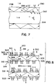
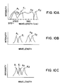
- Figs. 10A-10C Use of different fluorophores having selected absorption and emission spectra are illustrated in Figs. 10A-10C.
- the chart of Fig. 10A illustrates two fluorophores which have overlapping absorption spectra A 1 A 2 , such as for the dyes FITC and BPE. Both fluorophores can therefore be stimulated by a single excitation wavelength, indicated by arrow 370 between 500-505 nm.
- the FITC has an emission spectra E 1 which is different from emission spectra E 2 of BPE, and therefore two different output signals are generated.
- Fig. 10B The use of two fluorophores have different absorption and emission spectra is illustrated in Fig. 10B. Neither the absorption spectra A 1 nor the emission spectra E 1 overlap with the second absorption spectra A 2 or the emission spectra E 2 of the second fluorophore.
- the first fluorophore is FITC and the second fluorophore is Texas Red.
- Fig. 10C The use of two fluorophores in which the emission spectra E 1 overlaps the absorption spectra A 2 of the second fluorophore is illustrated in Fig. 10C.
- One such set of dyes is DPE and APC as described above for Fig. 9.
- Other combinations include BPE and Texas red or fluorocein.
- a sensor according to the invention can be implemented using a cone, hollow rod, a planar element, or other waveguide which presents two or more different optical surfaces.
- a sensor according to the invention can be implemented using a cone, hollow rod, a planar element, or other waveguide which presents two or more different optical surfaces.
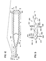
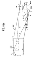
- the hollow rod 380, Fig. 11A, is combined with a conical launcher 382 which is similar to the conical sensor described in the cross-referenced patent application, "Evanescent Wave Sensorship and Apparatus".
- the launcher 382 includes an annular flange 384 which press-fits around the outside of the rod 380 to butt-couple the edge 386 of the rod 380 with the edge 388 of the launcher 382.
- a nonfluorescent epoxy may be used to join surfaces 386, 388 such as Epo-Tek 301 available from Epoxy Technology, Inc., Billerica, Massachusetts.
- Epo-Tek 301 epoxy is acceptable when the launcher 382 is formed of PMMA and the rod 380 is formed of silica glass.
- Acceptable dimensions of the launcher 382 are as follows when the rod 380 has an inner diameter I of 1.5 mm, an outer diameter F of 2.0 mm, and a wall thickness H of 0.25 mm.
- the launcher 282 has an overall length A of 4.45 mm and an effective length B of 4.25 mm.
- the overall length A includes length C of 0.2 mm for the flange 384.
- the thickness D of the flange 384 is 0.1 mm. Therefore, the launcher 382 has an overall diameter G of 2.2 mm and an effective diameter F of 2.0 mm.
- the radiation port 390 has a diameter E of 0.5 mm. Although the radiation port 390 is shown as planar, a convex or concave surface may instead be used to focus or defocus incoming radiation, respectively.
- the launcher 382 has a cone angle f of 10°.
- the launcher 382 has a thickness H of 0.25 mm, the same as that of the hollow rod 380.
- the path of light rays introduced at different positions on the radiation port 390 is illustrated by rays 392, 394.
- the ray 392 is first reflected from the outer surface of the hollow rod 380 at location 396 and the ray 394 is first reflected at location 398, thereby generating evanescent wave electromagnetic fields. It is desirable to generate as many internal reflections as possible so that a maximum amount of the evanescent wave electromagnetic fields are generated.
- Fig. 11B Calculation of the angles of the launcher 382 and the radiation introduced into it is shown schematically in Fig. 11B.
- the index of refraction n A of air is 1.0002
- the index n W for water is 1.3333
- the index n G of the silica glass sensor 380 is 1.4584
- the index n p of the PMMA launcher 382 is 1.4917.
- the object of the design is to produce an angle q which is equal to or greater than the critical angle established between the sensor 380 and the medium to be analyzed.
- the critical angle q is calculated according to the formula. 1.
- the critical angle q sin -1 (n W /n G )
- the critical angle q is calculated to be 66.095°.
- the entrance angle m is determined by subtracting the angle q from 90° and in this example is 23.904°.
- the critical angle j for the launcher 382 is calculated according to equation number 1 to be 42.106°.
- the actual angle of incidence i of the light ray 400 must therefore be greater than or equal to 42.106°.
- the incident angle h is calculated according to Snell's Law: 2.
- n P sin h n G sin m
- the incident angle h equals 23.338°.
- angles f and k are measured relative to reference line 402 which is perpendicular to the radiation port 390.
- the incoming light angle l is measured relative to the reference line 404 which is also perpendicular to the radiation port 390.
- angle k For light approaching the radiation port 390 at an angle l equals 0, angle k equals 0, and angle f is less than or equal to 1/2 angle h. Angle f in this example is therefore less than or equal to 11.669°.
- angle i is determined according to equation number 3 to be 76.662°.
- the cone angle f directly effects the incident angle l.
- An angle f decreases, angle l increases.
- the light ray 406 illustrates a path taken by radiation entering the radiation port 390 near its outer edge and at an angle l which is the opposite to that of ray 400.
- the path of ray 406 is undesirable because it inters the sensor 380 at a very large angle relative to the critical angle and therefore will have very few internal reflections. Therefore, it is desirable to have most of the light delivered at angle h.
- FIG. 12 An alternative launcher 410 is shown in Fig. 12.
- the launcher 410 is heated and drawn from a borosilicate microcapillary tube having an outer diameter of 1.5 mm and an inner diameter 1.15 mm. During drawing, the inner and outer surfaces of the launcher 410 are maintained approximately parallel to each other. These dimensions correspond to inner diameter R, outer diameter S which applied to length Q, which is 25.5 mm in this example.
- the launcher 410 has a tapered portion having a length N of 7 mm and a fully reduced diameter portion of a length K of 6.5 mm.
- the final diameter of radiation port 411 is 0.762 mm.
- the exit port 413 of the launcher 410 is butt-coupled with a 1.5 mm outer diameter corosilicate capillary tube which serves as a sensor according to the present invention.
- the paths of two rays 412, 414 are illustrated schematically. Excitation radiation is introduced through the radiation port 411 at the same angle as if the radiation were introduced directly into the sensor.
- the overall length J of sensor 410 is approximately 39 mm.
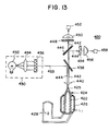
- An apparatus 420 according to the invention for delivering excitation radiation to a sensor 422 through a launcher 424 is shown in Fig. 13.
- the sensor 422 is installed in a first reservoir 426 which allows a first liquid L 1 to contact the outer surface of the sensor 422. Inside of the sensor 422 is connected to a second reservoir 428 which contains liquid L 2 that is drawn by capillary action into the inside of the sensor 422.
- the construction of the sensor or launcher should incorporate an appropriately placed vent hole for air escape on contact with the medium.
- Light source 430 produces coherent excitation light 432 at a first wavelength.
- the source 430 includes a tungsten lamp which produces noncolummated radiation that is collected by a lens 432 and passed through an interference filter 436 to produce the excitation wavelength 433.
- the excitation radiation 433 is reflected by first dichroic beam splitter 438 and is passed through launch lens 440 which focuses the radiation upon radiation port 425 of the launcher 424.
- the apparatus 420 is constructed to monitor two output wavelengths 442 and 444.
- the output radiation emerges through radiation port 425 and is directed by the lens 440 through the first beam splitter 428 to a second dicrylic beam splitter 446 which passes a first emission wavelength 442 and reflects the second output radiation 444 which is at a different wavelength.
- the first output wavelength 442 passes through interference filter 448 which blocks wavelengths other than those of interest.
- the radiation is focused by lens 450 upon first detector 452 which converts the first radiation output signal 442 to an electronic signal.
- the second output radiation 444 passes through an interference filter 454 and focusing lens 456, whereupon it impinges upon second detector 458 which produces a second electronic output signal.
- the actual excitation and emission wavelengths are selected as described above for Figs. 3-10C.
Claims (29)
- Capteur d'onde évanescente comprenant :a) un guide d'onde comportant au moins une première surface de propagation d'onde et une seconde surface de propagation d'onde, ledit guide d'onde étant conçu pour la propagation d'un signal ou de plusieurs signaux d'entrée de rayonnement le long dudit guide d'onde entre lesdites première et seconde surfaces, et pour l'émission d'un signal ou de plusieurs signaux de sortie de rayonnement,b) ladite première surface étant revêtue d'un réactif spécifique à une substance à analyser et pouvant recevoir un signal de rayonnement afin de détecter une première substance à analyser, etc) ladite seconde surface étant revêtue d'un second réactif spécifique à une substance à analyser, et un matériau de référence fluorescent ou bien un matériau de référence fluorescent dans lequel ladite seconde surface peut recevoir un signal de rayonnement afin de détecter au moins l'un d'une seconde substance à analyser et/ou d'une référence.
- Capteur selon la revendication 1, dans lequel ledit guide d'onde comprend un coeur creux comportant une surface interne (208) et une surface externe (204), l'une desdites surfaces interne et externe formant ladite première surface de propagation d'onde et l'autre desdites surfaces interne et externe formant ladite seconde surface de propagation d'onde.
- Capteur selon la revendication 1, dans lequel ledit guide d'onde comprend une coque (11) comportant un accès de rayonnement (12) à une première extrémité et une base (14) à une seconde extrémité, et comportant des surfaces de paroi intérieure et extérieure (20, 18) s'étendant entre l'accès de rayonnement et la base, l'une desdites surfaces intérieure et extérieure formant ladite première surface de propagation d'onde et l'autre desdites surfaces intérieure et extérieure formant ladite seconde surface de propagation d'onde.
- Capteur selon la revendication 1, dans lequel ledit guide d'onde comprend un élément plan comportant des surfaces supérieure et inférieure (340, 334), l'une desdites surfaces supérieure et inférieure formant ladite première surface de propagation d'onde et l'autre desdites surfaces supérieure et inférieure formant ladite seconde surface de propagation d'onde.
- Capteur selon l'une quelconque des revendications précédentes, dans lequel lesdites première et seconde surfaces de propagation d'onde propagent un rayonnement entre elles par une réflexion interne totale le long d'un axe de propagation, et lesdites surfaces sont pratiquement parallèles l'une à l'autre le long de l'axe de propagation.
- Capteur selon l'une quelconque des revendications précédentes, dans lequel un premier milieu est prévu pour la détection de la première substance à analyser dans celui-ci.
- Capteur selon l'une quelconque des revendications précédentes, dans lequel un second milieu est prévu pour la détection de la seconde substance à analyser ou de la référence dans celui-ci.
- Capteur selon l'une quelconque des revendications précédentes, dans lequel ladite première surface (204) comprend un premier revêtement réactif (202) comprenant un partenaire de liaison (210) de la première substance à analyser.
- Capteur selon la revendication 8, dans lequel ladite seconde surface (208) comprend un second revêtement réactif (206) comprenant un partenaire de liaison (214) d'une autre substance à analyser et/ou d'une référence dans lequel ladite autre substance à analyser est la seconde substance à analyser.
- Capteur selon la revendication 8 ou la revendication 9, dans lequel ledit premier revêtement réactif et/ou ledit second revêtement réactif est un anticorps immobilisé.
- Capteur selon la revendication 8 ou la revendication 9, dans lequel ledit premier revêtement réactif et/ou ledit second revêtement réactif est un antigène immobilisé.
- Capteur selon la revendication 8 ou la revendication 9, dans lequel ledit premier revêtement réactif est une enzyme.
- Capteur selon la revendication 8 ou la revendication 9, dans lequel ledit premier revêtement réactif et/ou ledit second revêtement réactif est un acide nucléique.
- Capteur selon les revendications 8 ou 9, dans lequel ledit premier revêtement réactif et/ou ledit second revêtement réactif est un récepteur.
- Capteur selon la revendication 8 ou la revendication 9, dans lequel ledit premier revêtement réactif et/ou ledit second revêtement réactif est une molécule de liaison.
- Capteur selon l'une quelconque des revendications précédentes, dans lequel ledit guide d'onde est transmetteur de la lumière qui peut exciter la fluorescence d'un marqueur fluorescent (222, 226) et est transmetteur du rayonnement fluorescent provenant du marqueur fluorescent (222, 226).
- Capteur selon la revendication 1, comprenant en outre un moyen destiné à isoler ladite seconde surface d'un milieu auquel ladite première surface est exposée.
- Capteur selon la revendication 17, dans lequel ledit moyen destiné à isoler comprend un gel.
- Capteur selon la revendication 17, dans lequel ledit moyen destiné à isoler comprend une matière solide.
- Capteur selon la revendication 19, dans lequel ledit moyen destiné à isoler comprend un copolymère de polytétrafluoroéthylène et d'hexafluoropropylène.
- Capteur selon l'une quelconque des revendications précédentes, dans lequel ledit signal lumineux représentant au moins l'une d'une seconde substance à analyser et/ou d'une référence présente une amplitude qui dépend de l'amplitude du rayonnement qui rentre à nouveau dans ladite première surface.
- Capteur selon l'une quelconque des revendications précédentes, lorsqu'elle dépend de la revendication 2, comprenant en outre un moyen (382, 410) destiné à délivrer le signal d'entrée lumineux audit coeur creux.
- Capteur selon la revendication 22, dans lequel ledit moyen destiné à délivrer comprend un élément de lanceur (382 ; 410) comportant un accès de rayonnement de petit diamètre (390 ; 412) à une première extrémité et un diamètre extérieur plus grand (388 ; 413) au niveau d'une seconde extrémité, qui correspond au diamètre extérieur dudit guide d'onde.
- Capteur selon la revendication 23 dans lequel ledit moyen destiné à délivrer (410) est un coeur creux allongé.
- Capteur selon la revendication 23, dans lequel ledit moyen destiné à délivrer (382) est un barreau allongé.
- Appareil destiné à analyser au moins un milieu, comprenant :un capteur d'onde évanescente (422) selon l'une quelconque des revendications 1 à 25,un moyen destiné à guider (438, 440) un signal d'entrée de lumière jusque dans le guide d'onde dudit capteur d'onde évanescente depuis une source de rayonnement de façon à ce que signal d'entrée se propage entre les première et seconde surfaces du guide d'onde, etun moyen destiné à guider (446, 450, 456) au moins un signal de sortie depuis ledit guide d'onde vers un moyen destiné à détecter (452, 458) le signal de sortie.
- Procédé consistant à doser au moins une substance à analyser dans au moins un milieu, comprenant :a) la fourniture d'un guide d'onde comportant au moins une première surface de propagation d'onde et une seconde surface de propagation d'onde ;b) l'immersion du guide d'onde dans au moins un milieu afin de le mettre en contact avec au moins l'une des première et seconde surfaces ;c) la propagation du rayonnement au travers du guide d'onde entre les première et seconde surfaces afin de générer des champs électromagnétiques d'ondes évanescentes à la fois au niveau des première et seconde surfaces afin d'illuminer le milieu, etd) détecter le rayonnement entrant à nouveau dans le guide d'onde et émis depuis le guide d'onde afin de doser la substance ou les substances à analyser, dans lequel ladite détection comprend la surveillance d'au moins deux signaux de sortie, un premier signal de sortie généré au niveau de la première surface et un second signal de sortie généré au niveau de la seconde surface.
- Procédé selon la revendication 27 comprenant le dosage spectrophotométrique de ladite au moins une substance à analyser dans au moins un milieu, dans lequel un revêtement réactif est disposé sur au moins l'une des première et seconde surfaces afin d'interagir avec une ou plusieurs substances à analyser ;dans lequel l'étape de propagation du rayonnement à travers le guide d'onde consiste également à générer des champs électromagnétiques d'ondes évanescentes afin d'illuminer la substance ou les substances à analyser et le revêtement réactif en interaction.
- Procédé selon la revendication 28, dans lequel le rayonnement qui se propage dans le guide d'onde induit une fluorescence lors de l'illumination de la substance ou des substances à analyser et du revêtement réactif en interaction, et la détection comprend la surveillance du rayonnement fluorescent émis à partir du guide d'onde.
Applications Claiming Priority (2)
| Application Number | Priority Date | Filing Date | Title |
|---|---|---|---|
| US07/711,783 US5340715A (en) | 1991-06-07 | 1991-06-07 | Multiple surface evanescent wave sensor with a reference |
| US711783 | 1991-06-07 |
Publications (3)
| Publication Number | Publication Date |
|---|---|
| EP0519623A2 EP0519623A2 (fr) | 1992-12-23 |
| EP0519623A3 EP0519623A3 (en) | 1993-06-09 |
| EP0519623B1 true EP0519623B1 (fr) | 1998-08-12 |
Family
ID=24859515
Family Applications (1)
| Application Number | Title | Priority Date | Filing Date |
|---|---|---|---|
| EP92305122A Expired - Lifetime EP0519623B1 (fr) | 1991-06-07 | 1992-06-04 | Système de palpeur avec surfaces multiples pour ondes amorties |
Country Status (5)
| Country | Link |
|---|---|
| US (1) | US5340715A (fr) |
| EP (1) | EP0519623B1 (fr) |
| JP (1) | JPH07181132A (fr) |
| CA (1) | CA2069539A1 (fr) |
| DE (1) | DE69226572T2 (fr) |
Cited By (3)
| Publication number | Priority date | Publication date | Assignee | Title |
|---|---|---|---|---|
| US8300993B2 (en) | 2009-03-02 | 2012-10-30 | Mbio Diagnostics, Inc. | Waveguide with integrated lens |
| US8331751B2 (en) | 2009-03-02 | 2012-12-11 | mBio Diagnositcs, Inc. | Planar optical waveguide with core of low-index-of-refraction interrogation medium |
| US9212995B2 (en) | 2009-03-02 | 2015-12-15 | Mbio Diagnostics, Inc. | System and method for detecting multiple molecules in one assay |
Families Citing this family (78)
| Publication number | Priority date | Publication date | Assignee | Title |
|---|---|---|---|---|
| US5935522A (en) * | 1990-06-04 | 1999-08-10 | University Of Utah Research Foundation | On-line DNA analysis system with rapid thermal cycling |
| US7081226B1 (en) | 1996-06-04 | 2006-07-25 | University Of Utah Research Foundation | System and method for fluorescence monitoring |
| US7273749B1 (en) | 1990-06-04 | 2007-09-25 | University Of Utah Research Foundation | Container for carrying out and monitoring biological processes |
| US5726064A (en) * | 1990-11-22 | 1998-03-10 | Applied Research Systems Ars Holding Nv | Method of assay having calibration within the assay |
| CA2069537A1 (fr) * | 1991-06-07 | 1992-12-08 | Thomas A. Cook | Systeme d'analyse a sorties multiples utilisant un capteur d'ondes evanescentes |
| GB9212302D0 (en) * | 1992-06-10 | 1992-07-22 | Applied Research Systems | Method for improving measurement precision in evanescent wave optical biosensor assays |
| DE4307042A1 (de) * | 1993-03-05 | 1994-09-08 | S & L Ges Fuer Wissenschaftlic | Verfahren zum optischen qualitativen und quantitativen Nachweis von Molekülen, Biomolekülen und Mikroorganismen |
| ATE209782T1 (de) * | 1993-05-18 | 2001-12-15 | Univ Utah Res Found | Vorrichtung und verfahren fuer homogene multianalyt-immuno-assays |
| US5919712A (en) | 1993-05-18 | 1999-07-06 | University Of Utah Research Foundation | Apparatus and methods for multi-analyte homogeneous fluoro-immunoassays |
| US5677196A (en) * | 1993-05-18 | 1997-10-14 | University Of Utah Research Foundation | Apparatus and methods for multi-analyte homogeneous fluoro-immunoassays |
| US5737457A (en) * | 1994-02-25 | 1998-04-07 | Fci - Fiberchem, Inc. | Chip level waveguide sensor |
| WO1995026416A1 (fr) * | 1994-03-25 | 1995-10-05 | Research Corporation Technologies, Inc. | Procede de diagnostic par biocapteurs d'acide nucleique |
| US5814565A (en) * | 1995-02-23 | 1998-09-29 | University Of Utah Research Foundation | Integrated optic waveguide immunosensor |
| US5745231A (en) * | 1995-06-12 | 1998-04-28 | American Research Corporation Of Virginia | Method of fluorescence analysis comprising evanescent wave excitation and out-of-plane photodetection |
| US6887430B1 (en) * | 1996-01-26 | 2005-05-03 | Kyoto Dai-Ichi Kagaku Co., Ltd. | Apparatus for immune analysis |
| WO1997032212A1 (fr) * | 1996-03-01 | 1997-09-04 | Beckman Instruments, Inc. | Systeme d'essais multiples simultanes de fixation de ligands |
| US6611634B2 (en) | 1996-03-19 | 2003-08-26 | University Of Utah Research Foundation | Lens and associatable flow cell |
| US5721795A (en) * | 1996-05-17 | 1998-02-24 | Tir Technologies, Inc. | High efficiency ejection of light from optical wave guide, by holographically produced light scattering means |
| US6103535A (en) | 1996-05-31 | 2000-08-15 | University Of Maryland | Optical fiber evanescent field excited fluorosensor and method of manufacture |
| ATE428801T1 (de) | 1996-06-04 | 2009-05-15 | Univ Utah Res Found | Überwachung der hybridisierung während pcr |
| DE69738605T2 (de) * | 1996-06-04 | 2009-04-30 | University Of Utah Research Foundation, Salt Lake City | Behälter zum Durchführen und Beobachten biologischer Prozesse |
| US5780251A (en) * | 1996-06-27 | 1998-07-14 | Fci Fiberchem, Inc. | Ultrasensitive single-step, solid-state competitive immunoassay sensor with interference modifier and/or gel layer |
| US5832165A (en) * | 1996-08-28 | 1998-11-03 | University Of Utah Research Foundation | Composite waveguide for solid phase binding assays |
| US5828798A (en) * | 1996-09-09 | 1998-10-27 | Hopenfeld; Joram | Looped fiber-optic sensor for the detection of substances |
| DE19651935A1 (de) * | 1996-12-14 | 1998-06-18 | Ruckstuhl Thomas | Detektionssystem für den optischen Nachweis von Molekülen |
| US5776785A (en) * | 1996-12-30 | 1998-07-07 | Diagnostic Products Corporation | Method and apparatus for immunoassay using fluorescent induced surface plasma emission |
| US5859937A (en) * | 1997-04-04 | 1999-01-12 | Neomecs Incorporated | Minimally invasive sensor |
| US6025189A (en) * | 1997-05-14 | 2000-02-15 | 3M Innovative Properties Company | Apparatus for reading a plurality of biological indicators |
| WO1998058079A1 (fr) * | 1997-06-18 | 1998-12-23 | Krull Ulrich J | Diagnostic par biocapteurs a acides nucleiques |
| US6222619B1 (en) | 1997-09-18 | 2001-04-24 | University Of Utah Research Foundation | Diagnostic device and method |
| DE19747572C1 (de) * | 1997-10-28 | 1999-04-08 | Inst Chemo Biosensorik | Vorrichtung und Verfahren zur Durchführung von Fluoreszenzimmuntests |
| CN1292087A (zh) * | 1998-02-02 | 2001-04-18 | 西格雷特生物科学有限公司 | 检测分子结合作用的方法和仪器 |
| US6485905B2 (en) * | 1998-02-02 | 2002-11-26 | Signature Bioscience, Inc. | Bio-assay device |
| US6338968B1 (en) * | 1998-02-02 | 2002-01-15 | Signature Bioscience, Inc. | Method and apparatus for detecting molecular binding events |
| US6395480B1 (en) | 1999-02-01 | 2002-05-28 | Signature Bioscience, Inc. | Computer program and database structure for detecting molecular binding events |
| US6020207A (en) * | 1998-06-17 | 2000-02-01 | World Precision Instruments, Inc. | Optical analysis technique and sensors for use therein |
| US6429023B1 (en) | 1998-07-20 | 2002-08-06 | Shayda Technologies, Inc. | Biosensors with polymeric optical waveguides |
| US6463187B1 (en) | 1998-08-24 | 2002-10-08 | Empirical Technologies Corporation | Variable coupler fiberoptic sensor and sensing apparatus using the sensor |
| US6687424B1 (en) | 1998-08-24 | 2004-02-03 | Empirical Technologies Corporation | Sensing pad assembly employing variable coupler fiberoptic sensor |
| US6723054B1 (en) | 1998-08-24 | 2004-04-20 | Empirical Technologies Corporation | Apparatus and method for measuring pulse transit time |
| US6907148B2 (en) | 1998-08-24 | 2005-06-14 | Empirical Technologies Corporation | Sensing apparatus employing variable coupler fiberoptic sensor |
| US6300638B1 (en) | 1998-11-12 | 2001-10-09 | Calspan Srl Corporation | Modular probe for total internal reflection fluorescence spectroscopy |
| USD426783S (en) * | 1999-04-19 | 2000-06-20 | University Of Utah Research Foundation | Waveguide lens |
| US6254830B1 (en) | 1999-11-05 | 2001-07-03 | The Board Of Governors For Higher Education, State Of Rhode Island And Providence Plantations | Magnetic focusing immunosensor for the detection of pathogens |
| US7384797B1 (en) * | 2000-10-12 | 2008-06-10 | University Of Utah Research Foundation | Resonant optical cavities for high-sensitivity high-throughput biological sensors and methods |
| WO2002033005A2 (fr) * | 2000-10-19 | 2002-04-25 | Trans Photonics, L.L.C. | Nouveaux composants chromophoriques polyaryl-substitues |
| DE60231960D1 (de) * | 2001-01-23 | 2009-05-28 | Univ Dublin City | Lumineszenz-detektor |
| JP3429282B2 (ja) * | 2001-02-02 | 2003-07-22 | リサーチ・インターナショナル・インコーポレーテッド | 自動化されたシステム、及びサンプルの分析方法 |
| US6974673B2 (en) * | 2001-09-24 | 2005-12-13 | Veridian Systems Division | Coupled capillary fiber based waveguide biosensor |
| US7189361B2 (en) * | 2001-12-19 | 2007-03-13 | 3M Innovative Properties Company | Analytical device with lightguide Illumination of capillary and microgrooves arrays |
| US20040081384A1 (en) * | 2002-10-25 | 2004-04-29 | Datesman Aaron M. | Multiple-mode planar-waveguide sensor, fabrication materials and techniques |
| AU2002952384A0 (en) * | 2002-10-31 | 2002-11-14 | Swinburne University Of Technology | Structures |
| US7545496B2 (en) * | 2003-06-25 | 2009-06-09 | Koninklijke Philips Electronics N.V. | Support with a surface structure for sensitive evanescent-field detection |
| US7496392B2 (en) * | 2003-11-26 | 2009-02-24 | Becton, Dickinson And Company | Fiber optic device for sensing analytes |
| US7283245B2 (en) * | 2004-01-20 | 2007-10-16 | General Electric Company | Handheld device with a disposable element for chemical analysis of multiple analytes |
| US7496245B2 (en) * | 2004-08-20 | 2009-02-24 | Research International, Inc. | Misalignment compensating optical sensor and method |
| US20060141527A1 (en) * | 2004-12-29 | 2006-06-29 | Caracci Stephen J | Method for creating a reference region and a sample region on a biosensor and the resulting biosensor |
| US7629173B2 (en) | 2004-12-29 | 2009-12-08 | Corning Incorporated | Optical reader system and method for monitoring and correcting lateral and angular misalignments of label independent biosensors |
| US7604984B2 (en) * | 2004-12-29 | 2009-10-20 | Corning Incorporated | Spatially scanned optical reader system and method for using same |
| US8173973B2 (en) * | 2005-10-06 | 2012-05-08 | Nanyang Technological University | Eliminating fluorescence background noise |
| EP2002240A1 (fr) * | 2006-03-07 | 2008-12-17 | Nanyang Technological University | Dispositif de dosage immunologique microfluidique |
| US9976192B2 (en) | 2006-03-10 | 2018-05-22 | Ldip, Llc | Waveguide-based detection system with scanning light source |
| US9528939B2 (en) | 2006-03-10 | 2016-12-27 | Indx Lifecare, Inc. | Waveguide-based optical scanning systems |
| US7651869B2 (en) * | 2006-03-14 | 2010-01-26 | Research International, Inc. | Optical assay apparatus and methods |
| US20070264155A1 (en) * | 2006-05-09 | 2007-11-15 | Brady Michael D | Aerosol jet deposition method and system for creating a reference region/sample region on a biosensor |
| JP5748319B2 (ja) | 2006-07-25 | 2015-07-15 | ザ ボード オブ トラスティーズ オブ ザ レランド スタンフォード ジュニア ユニバーシティー | 中空コアのファイバテーパを用いる装置および方法 |
| JP2008102117A (ja) * | 2006-09-21 | 2008-05-01 | Fujifilm Corp | 表面プラズモン増強蛍光センサおよび蛍光検出方法 |
| WO2008097199A1 (fr) * | 2007-02-06 | 2008-08-14 | Nanyang Technological University | Appareil et procédé d'analyse d'un échantillon fluorescent disposé sur un substrat |
| US20090326344A1 (en) * | 2008-06-27 | 2009-12-31 | Tyco Healthcare Group Lp | System and Method for Optical Continuous Detection of an Analyte In Bloodstream |
| US9658222B2 (en) | 2009-03-02 | 2017-05-23 | Mbio Diagnostics, Inc. | Planar waveguide based cartridges and associated methods for detecting target analyte |
| JP5285471B2 (ja) * | 2009-03-11 | 2013-09-11 | 富士フイルム株式会社 | 全反射照明型センサチップ、その製造方法およびそれを用いたセンシング方法 |
| WO2012037369A1 (fr) * | 2010-09-15 | 2012-03-22 | Mbio Diagnostics, Inc. | Système et procédé servant à détecter des molécules multiples en une analyse |
| US20140106336A1 (en) * | 2010-12-07 | 2014-04-17 | Colorado School Of Mines | Detection of Magnetic-Field-Concentrated Analytes in a Lateral Flow Capillary |
| US9041408B2 (en) * | 2013-01-16 | 2015-05-26 | Hrl Laboratories, Llc | Removable surface-wave networks for in-situ material health monitoring |
| CA3209249A1 (fr) * | 2013-02-18 | 2014-08-21 | Theranos Ip Company, Llc | Analyse d'images et mesure d'echantillons biologiques |
| US10018566B2 (en) | 2014-02-28 | 2018-07-10 | Ldip, Llc | Partially encapsulated waveguide based sensing chips, systems and methods of use |
| WO2016138427A1 (fr) | 2015-02-27 | 2016-09-01 | Indx Lifecare, Inc. | Système de détection à guide d'ondes à source de lumière à balayage |
| CN109799202B (zh) * | 2019-01-16 | 2023-11-24 | 黄文佳 | 一种利用电磁波反射成像图进行物质分析的装置及方法 |
Family Cites Families (15)
| Publication number | Priority date | Publication date | Assignee | Title |
|---|---|---|---|---|
| US3604927A (en) * | 1966-11-16 | 1971-09-14 | Block Engineering | Total reflection fluorescence spectroscopy |
| US4050895A (en) * | 1975-09-26 | 1977-09-27 | Monsanto Research Corporation | Optical analytical device, waveguide and method |
| US4582809A (en) * | 1982-06-14 | 1986-04-15 | Myron J. Block | Apparatus including optical fiber for fluorescence immunoassay |
| US4558014A (en) * | 1983-06-13 | 1985-12-10 | Myron J. Block | Assay apparatus and methods |
| AT383684B (de) * | 1984-09-17 | 1987-08-10 | Avl Verbrennungskraft Messtech | Anordnung zur fluoreszenzoptischen messung von stoffkonzentrationen in einer probe |
| US4775637A (en) * | 1984-12-10 | 1988-10-04 | Purtec Limited | An immunoassay apparatus having at least two waveguides and method for its use |
| US4716121A (en) * | 1985-09-09 | 1987-12-29 | Ord, Inc. | Fluorescent assays, including immunoassays, with feature of flowing sample |
| US4671938A (en) * | 1985-09-09 | 1987-06-09 | Ciba-Corning Diagnostics, Corp. | Immunoassay apparatus |
| US4852967A (en) * | 1986-03-25 | 1989-08-01 | Ciba Corning Diagnostics Corp. | Evanescent wave sensors |
| US5001051A (en) * | 1986-12-12 | 1991-03-19 | Regents Of The University Of California | Dose critical in-vivo detection of anti-cancer drug levels in blood |
| US4846548A (en) * | 1987-05-06 | 1989-07-11 | St&E, Inc. | Fiber optic which is an inherent chemical sensor |
| AU604364B2 (en) * | 1987-08-13 | 1990-12-13 | Dow Chemical Company, The | Sulfur dioxide removal from gas streams using hydroxyalkyl substituted piperazinones |
| US4842783A (en) * | 1987-09-03 | 1989-06-27 | Cordis Corporation | Method of producing fiber optic chemical sensors incorporating photocrosslinked polymer gels |
| US4893894A (en) * | 1988-04-29 | 1990-01-16 | Mine Safety Appliances Company | Evanescent sensor |
| US5156976A (en) * | 1991-06-07 | 1992-10-20 | Ciba Corning Diagnostics Corp. | Evanescent wave sensor shell and apparatus |
-
1991
- 1991-06-07 US US07/711,783 patent/US5340715A/en not_active Expired - Fee Related
-
1992
- 1992-05-26 CA CA002069539A patent/CA2069539A1/fr not_active Abandoned
- 1992-06-04 EP EP92305122A patent/EP0519623B1/fr not_active Expired - Lifetime
- 1992-06-04 DE DE69226572T patent/DE69226572T2/de not_active Expired - Fee Related
- 1992-06-08 JP JP4147228A patent/JPH07181132A/ja active Pending
Cited By (4)
| Publication number | Priority date | Publication date | Assignee | Title |
|---|---|---|---|---|
| US8300993B2 (en) | 2009-03-02 | 2012-10-30 | Mbio Diagnostics, Inc. | Waveguide with integrated lens |
| US8331751B2 (en) | 2009-03-02 | 2012-12-11 | mBio Diagnositcs, Inc. | Planar optical waveguide with core of low-index-of-refraction interrogation medium |
| US8606066B2 (en) | 2009-03-02 | 2013-12-10 | Mbio Diagnostics, Inc. | Planar optical waveguide with core of low-index-of-refraction interrogation medium |
| US9212995B2 (en) | 2009-03-02 | 2015-12-15 | Mbio Diagnostics, Inc. | System and method for detecting multiple molecules in one assay |
Also Published As
| Publication number | Publication date |
|---|---|
| DE69226572D1 (de) | 1998-09-17 |
| DE69226572T2 (de) | 1999-03-11 |
| CA2069539A1 (fr) | 1992-12-08 |
| JPH07181132A (ja) | 1995-07-21 |
| EP0519623A3 (en) | 1993-06-09 |
| US5340715A (en) | 1994-08-23 |
| EP0519623A2 (fr) | 1992-12-23 |
Similar Documents
| Publication | Publication Date | Title |
|---|---|---|
| EP0519623B1 (fr) | Système de palpeur avec surfaces multiples pour ondes amorties | |
| US5156976A (en) | Evanescent wave sensor shell and apparatus | |
| US4880752A (en) | Dielectric waveguide sensors and their use in immunoassays | |
| FI76432B (fi) | Foerfarande och anordning foer bestaemning av element i loesning med en ljusledare. | |
| US5814565A (en) | Integrated optic waveguide immunosensor | |
| CA1266826A (fr) | Appareil de dosage | |
| US4844869A (en) | Immunoassay apparatus | |
| US5350697A (en) | Scattered light detection apparatus | |
| USRE33064E (en) | Method for the determination of species in solution with an optical wave-guide | |
| US6558958B1 (en) | Optical fiber evanescent field excited fluorosensor and method of manufacture | |
| EP0184600B1 (fr) | Méthode pour la détermination optique de paramètres d'espèces chimiques dans un échantillon liquide | |
| US5525466A (en) | Multiple output referencing system for evanescent wave sensor | |
| JPH07218422A (ja) | 剛性管状導光体とその導光体を用いた水性液体試料の 吸光測定方法及びその装置 | |
| EP0353937A1 (fr) | Procédé d'essai | |
| JP2007501403A (ja) | 白色光反射干渉の分光変化規則に基づく光ファイバアレイバイオチップ | |
| EP0175585B1 (fr) | Capteurs diélectriques en guides d'ondes et leur application pour essais immunologiques | |
| Squillante | Applications of fiber-optic evanescent wave spectroscopy | |
| JPS62123358A (ja) | 光フアイバ型免疫センサ | |
| Slovacek et al. | Application of a plastic evanescent-wave sensor to immunological measurements of CKMB | |
| CA1269546A (fr) | Capteurs a guidage d'ondes dielectriques et leur utilisation dans les dosages immunologiques | |
| JPH01221666A (ja) | 免疫検査装置および免疫検査方法 | |
| NO161945B (no) | Fremgangsmaate og apparat for bestemmelse av stoffer i opploesning med en optisk boelgeleder. |
Legal Events
| Date | Code | Title | Description |
|---|---|---|---|
| PUAI | Public reference made under article 153(3) epc to a published international application that has entered the european phase |
Free format text: ORIGINAL CODE: 0009012 |
|
| AK | Designated contracting states |
Kind code of ref document: A2 Designated state(s): CH DE ES FR GB IT LI |
|
| PUAL | Search report despatched |
Free format text: ORIGINAL CODE: 0009013 |
|
| AK | Designated contracting states |
Kind code of ref document: A3 Designated state(s): CH DE ES FR GB IT LI |
|
| 17P | Request for examination filed |
Effective date: 19931117 |
|
| 17Q | First examination report despatched |
Effective date: 19960213 |
|
| GRAG | Despatch of communication of intention to grant |
Free format text: ORIGINAL CODE: EPIDOS AGRA |
|
| GRAG | Despatch of communication of intention to grant |
Free format text: ORIGINAL CODE: EPIDOS AGRA |
|
| GRAH | Despatch of communication of intention to grant a patent |
Free format text: ORIGINAL CODE: EPIDOS IGRA |
|
| GRAH | Despatch of communication of intention to grant a patent |
Free format text: ORIGINAL CODE: EPIDOS IGRA |
|
| GRAA | (expected) grant |
Free format text: ORIGINAL CODE: 0009210 |
|
| AK | Designated contracting states |
Kind code of ref document: B1 Designated state(s): CH DE ES FR GB IT LI |
|
| PG25 | Lapsed in a contracting state [announced via postgrant information from national office to epo] |
Ref country code: LI Free format text: LAPSE BECAUSE OF FAILURE TO SUBMIT A TRANSLATION OF THE DESCRIPTION OR TO PAY THE FEE WITHIN THE PRESCRIBED TIME-LIMIT Effective date: 19980812 Ref country code: FR Free format text: LAPSE BECAUSE OF FAILURE TO SUBMIT A TRANSLATION OF THE DESCRIPTION OR TO PAY THE FEE WITHIN THE PRESCRIBED TIME-LIMIT Effective date: 19980812 Ref country code: ES Free format text: THE PATENT HAS BEEN ANNULLED BY A DECISION OF A NATIONAL AUTHORITY Effective date: 19980812 Ref country code: CH Free format text: LAPSE BECAUSE OF FAILURE TO SUBMIT A TRANSLATION OF THE DESCRIPTION OR TO PAY THE FEE WITHIN THE PRESCRIBED TIME-LIMIT Effective date: 19980812 |
|
| REG | Reference to a national code |
Ref country code: CH Ref legal event code: EP |
|
| REF | Corresponds to: |
Ref document number: 69226572 Country of ref document: DE Date of ref document: 19980917 |
|
| EN | Fr: translation not filed | ||
| REG | Reference to a national code |
Ref country code: CH Ref legal event code: PL |
|
| PLBE | No opposition filed within time limit |
Free format text: ORIGINAL CODE: 0009261 |
|
| STAA | Information on the status of an ep patent application or granted ep patent |
Free format text: STATUS: NO OPPOSITION FILED WITHIN TIME LIMIT |
|
| 26N | No opposition filed | ||
| PGFP | Annual fee paid to national office [announced via postgrant information from national office to epo] |
Ref country code: DE Payment date: 20000518 Year of fee payment: 9 |
|
| PGFP | Annual fee paid to national office [announced via postgrant information from national office to epo] |
Ref country code: GB Payment date: 20000519 Year of fee payment: 9 |
|
| PG25 | Lapsed in a contracting state [announced via postgrant information from national office to epo] |
Ref country code: GB Free format text: LAPSE BECAUSE OF NON-PAYMENT OF DUE FEES Effective date: 20010604 |
|
| GBPC | Gb: european patent ceased through non-payment of renewal fee |
Effective date: 20010604 |
|
| PG25 | Lapsed in a contracting state [announced via postgrant information from national office to epo] |
Ref country code: DE Free format text: LAPSE BECAUSE OF NON-PAYMENT OF DUE FEES Effective date: 20020403 |
|
| PG25 | Lapsed in a contracting state [announced via postgrant information from national office to epo] |
Ref country code: IT Free format text: LAPSE BECAUSE OF NON-PAYMENT OF DUE FEES;WARNING: LAPSES OF ITALIAN PATENTS WITH EFFECTIVE DATE BEFORE 2007 MAY HAVE OCCURRED AT ANY TIME BEFORE 2007. THE CORRECT EFFECTIVE DATE MAY BE DIFFERENT FROM THE ONE RECORDED. Effective date: 20050604 |