EP0516296B1 - Programmierungsverfahren für Speicheranordnungen mit schwebendem Gate. - Google Patents
Programmierungsverfahren für Speicheranordnungen mit schwebendem Gate. Download PDFInfo
- Publication number
- EP0516296B1 EP0516296B1 EP92304071A EP92304071A EP0516296B1 EP 0516296 B1 EP0516296 B1 EP 0516296B1 EP 92304071 A EP92304071 A EP 92304071A EP 92304071 A EP92304071 A EP 92304071A EP 0516296 B1 EP0516296 B1 EP 0516296B1
- Authority
- EP
- European Patent Office
- Prior art keywords
- programming
- voltage
- volts
- floating gate
- read
- Prior art date
- Legal status (The legal status is an assumption and is not a legal conclusion. Google has not performed a legal analysis and makes no representation as to the accuracy of the status listed.)
- Expired - Lifetime
Links
Images

Classifications
-
- G—PHYSICS
- G11—INFORMATION STORAGE
- G11C—STATIC STORES
- G11C16/00—Erasable programmable read-only memories
- G11C16/02—Erasable programmable read-only memories electrically programmable
- G11C16/06—Auxiliary circuits, e.g. for writing into memory
- G11C16/10—Programming or data input circuits
Definitions
- This invention relates to floating gate memory devices, and more particularly to methods of programming such memory devices.
- the invention is pertinent to floating gate devices with separately optimized read and programming transistors coupled by a common floating gate, and which further are programmed by gate currents in the programming-optimized transistor. See, for example, B. Eitan et al. "Hot-Electron Injection into the Oxide in n-Channel MOS Devices", IEEE Transactions on Electron Devices , Vol. ED-28, No. 3, March 1981, pp. 328-40. US-A-4 663 740 discloses a conventional method of programming floating gate devices in accordance with the preamble of claim 1. The invention will be fully understood from the following explanation of it in the context of metal oxide semiconductor ("MOS”) erasable programmable read-only memory (“EPROM”) devices.
- MOS metal oxide semiconductor
- EPROM erasable programmable read-only memory
- a typical MOS EPROM device which is programmable in accordance with the method of this invention has a control gate (sometimes referred to simply as the gate), a floating gate, a source and drain pair for programming the device, and a source and drain pair for reading the programmed state of the device.
- the device is conventionally programmed by applying a relatively high voltage (e.g., 15 volts) to the gate and a somewhat lower voltage (e.g., 8 volts) to the programming drain, while holding the programming source at ground potential (i.e., 0 volts).
- Capacitive coupling between the control gate and the floating gate causes a change in the potential of the floating gate when the potential of the control gate is changed. For example, if the capacitive divide or coupling ratio is assumed to be 0.7 and both the control gate and the floating gate are initially at 0 volts, then raising the control gate to 15 volts causes the floating gate potential to rise to 10.5 volts.
- the programming transistor's channel begins to conduct a substantial current.
- the capacitive divider causes a 10.5 volt drop in potential from 6.5 volts to -4 volts on the floating gate.
- the floating gate transistor is an NMOS transistor with a threshold voltage of about 1 volt, the floating gate transistor is non-conducting.
- the control gate is raised to 5 volts, there results a 3.5 volt rise on the floating gate to -0.5 voltage.
- the programmed transistor therefore remains off. In other words, the read channel of a programmed device is always off regardless of the normal logic level (0 or 5 volts) applied to the gate of the device.
- the read channel of the device is on or off depending on whether 5 volts or 0 volts, respectively, is applied to the gate of the device because the floating gate potential is respectively 3.5 volts (above the threshold) or 0 volts (below the threshold).
- FIG. 1 is a simplified schematic diagram of an illustrative floating gate memory device which can be programmed in accordance with the method of this invention.
- FIG. 2 is a chart of various possible voltages in the floating gate memory device shown in FIG. 1 during conventional programming (first line) and during programming in accordance with this invention (subsequent lines).
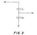
- FIG. 3 is a simplified schematic diagram of a conventional capacitive divider network.
- a typical floating gate memory device 10 programmable in accordance with this invention includes a gate 12 to which electrical potential can be applied via gate lead 14, a write or programming channel 30 connected between a programming source 32 and a programming drain 34, and a read channel 40 connected between a read source 42 and a read drain 44.
- Device 10 also includes floating gate 20 which is not an externally accessible electrode (i.e., potential cannot be directly applied to floating gate 20).
- a relatively high voltage such as 15 volts is applied to gate 12 via lead 14
- a somewhat lower voltage such as 8 volts is applied to programming drain 34
- programming source 32 is connected to ground (0 volts)
- read source 42 and drain 44 are not used and are customarily connected to ground.
- the inherent capacitive coupling between gate 12 and floating gate 20 initially raises the potential of floating gate 20 to a predetermined fraction of the gate 12 potential.
- the potential of floating gate 20 may initially be approximately 0.7 times the gate 12 potential (e.g., 10.5 volts).
- this negative charge is large enough, it makes it impossible for either 0 or 5 volts on gate 12 during normal logical operation of the device to raise the potential on floating gate 20 high enough for the floating poly transistor to turn on.
- the floating poly transistor has a threshold voltage of about 1 volt, so floating gate 20 would need to rise from -4 volts to 1 volt just to begin to allow the read channel to begin to conduct. This would require gate 12 to rise by 0 + (1 - (-4))/0.7 or 7.1 volts. Because 7.1 volts is outside of the 5 volt operating range of the circuit in end use, the transistor effectively cannot be turned on.
- read source 42 is connected to ground (0 volts)
- 5 volts is applied to read drain 44
- write channel 30 is not used (i.e., its source 32 and drain 34 are connected to ground)
- gate 12 is switched between 0 volts and 5 volts.
- a "programmed” device 10 therefore remains off at all times during normal logical operation. If device 10 is left “unprogrammed” (i.e., no charge is put on floating gate 20), then during normal logical operation, read channel 40 is off when gate 12 is at 0 volts and on (i.e., conducting) when gate 12 is at 5 volts.
- Device 10 must be at least a predetermined minimum size in order to be able to withstand the relatively high voltage (e.g., 15 volts) conventionally used during programming.
- These size limitations are both vertical dimensions (dielectric thicknesses) and planar dimensions such as channel length and spacings of electrodes.
- the dielectric thicknesses are limited by dielectric breakdown (units are volts/cm) when the voltage divided by the thickness exceeds about 10 7 volts/cm.
- the lateral dimensions are limited by the process technology limitations, but the larger the voltage difference between two diffusions, the larger the space required between them.
- floating gate 20 cannot be made to store sufficient charge to prevent read channel 40 from conducting when gate 12 is raised to 5 volts during normal logical operation.
- the need to program device 10 has therefore heretofore limited the device size reductions available.
- the present invention makes it possible to substantially lower the programming voltage which must be applied to gate 12 in order to raise floating gate 20 to the potential required to attract sufficient hot electrons to program the device. This is accomplished by applying a positive voltage to read source 42 and read drain 44 during programming.
- the inherent capacitive coupling between read channel 40 and floating gate 20 adds to the inherent capacitive coupling between gate 12 and floating gate 20. Accordingly, the programming potential applied to elements 42 and 44 allows the programming potential applied to gate 12 to be reduced, thereby allowing device 10 to be made smaller than would otherwise be possible.
- FIG. 2 is a table showing various illustrative values of V12 (the potential applied to gate 12), V4244 (the potential applied to read source 42 and read drain 44 in accordance with this invention), and the resulting V20 (the potential on floating gate 20) during programming, on the assumption that the inherent capacitive coupling between elements 12 and 20 is a factor of 0.7 and the inherent capacitive coupling between elements 20 and 40 is 0.3. (In all cases the conventional voltages described above are applied to write source 32 and write drain 34.) The first line in FIG. 2 shows the conventional strategy of applying 15 volts to gate 12 and not using read channel 40 during programming. The resulting initial potential on floating gate 20 is therefore 10.5 volts, which, as described above, produces satisfactory programming of device 10.
- the second line of FIG. 2 is an example of programming in accordance with this invention.
- the potential applied to gate 12 is reduced to 12.5 volts.
- the potential applied to read source 42 and read drain 44 is 5 volts.
- the third line of FIG. 2 shows another example of programming in accordance with this invention.
- 11 volts is applied to gate 12 and 8 volts is applied to read source 42 and read drain 44.
- the resulting initial potential on floating gate 20 is 10.1 volts, which will again produce satisfactory programming of device 10.
- Programming time may be reduced by a factor on the order of 5 (i.e., only one-fifth the programming time may be required) or 10 (i.e., only one-tenth the programming time may be required) in this way.
- Various combinations of reduced programming voltage and reduced programming time may also be employed.
- the fifth line of FIG. 2 shows the use of 14 volts applied to gate 12 with 5 volts applied to read source 42 and read drain 44 to produce an initial potential of 11.3 volts on floating gate 20. As compared to conventional programming (FIG. 2, line 1), this is a one-volt decrease in programming potential, combined with considerably faster programming (because V20 is initially substantially higher).
Landscapes
- Read Only Memory (AREA)
- Non-Volatile Memory (AREA)
Claims (13)
- Programmierungsverfahren für ein Speichergerät, das einen Gateanschluß (12), einen Programmierkanal (30), der zwischen einem Programmierquellenanschluß (32) und einem Programmiersenkenanschluß (34) geschaltet ist, einen Lesekanal (40), der zwischen einen Lesequellenanschluß (42) und einen Lesesenkenanschluß (44) geschaltet ist, und ein schwimmendes Gate (20), das kapazitiv an den Gateanschluß (12) und an den Lesekanal (40) gekoppelt ist, wobei das Verfahren die folgenden Schritte aufweist:Anlegen einer ersten Programmierspannung (VG) an den Gateanschluß (12);Anlegen einer zweiten Programmierspannung an den Programmierquellenanschluß (32);Anlegen einer dritten Programmierspannung an den Programmiersenkenanschluß (34);Anlegen einer vierten Programmierspannung an den Lesequellenanschluß (42),dadurch gekennzeichnet, daß
eine fünfte Programmierspannung (V42 44) an den Lesesenkenanschluß angelegt ist, wobei die erste, dritte, vierte und fünfte Programmierspannung eine vorbestimmte Polarität in bezug auf die zweite Programmierspannung aufweisen. - Verfahren nach Anspruch 1, wobei die zweite Programmierspannung auf Erdpotential liegt und jede der ersten, dritten, vierten und fünften Programmierspannung positiv ist.
- Verfahren nach Anspruch 1, wobei die vierte und fünfte Programmierspannung im wesentlichen gleich sind.
- Verfahren nach Anspruch 2, wobei die erste Programmierspannung größer als die dritte Programmierspannung ist und wobei die dritte Programmierspannung größer als die vierte und die fünfte Progammierspannung ist.
- Verfahren nach Anspruch 4, wobei die vierte und fünfte Programmierspannung im wesentlichen gleich sind.
- Verfahren nach Anspruch 1, wobei das Speichergerät ein MOS EPROM-Gerät ist, die erste, dritte, vierte und fünfte Programmierspannungen positiv sind und wobei die zweite Programmierspannung das Erdpotential ist.
- Verfahren nach Anspruch 6, wobei die erste Programmierspannung größer als die dritte Programmierspannung ist und wobei die vierte und fünfte Programmierspannung im wesentlichen gleich sind.
- Verfahren nach Anspruch 7, wobei die vierte und fünfte Programmierspannung kleiner als die dritte Programmierspannung sind.
- Verfahren nach Anspruch 8, wobei die erste Programmierspannung ungefähr 15 Volt beträgt, die dritte Programmierspannung ungefähr 8 Volt beträgt und wobei die vierte und fünfte Programmierspannung ungefähr 5 Volt beträgt.
- Verfahren nach Anspruch 8, wobei die erste Programmierspannung wesentlich kleiner als 15 Volt ist, die dritte Programmierspannung ungefähr 8 Volt ist und wobei die vierte und fünfte Programmierspannung ungefähr 5 Volt beträgt.
- Verfahren nach Anspruch 10, wobei die erste Programmierspannung mindestens 1 Volt geringer als 15 Volt ist.
- Verfahren nach Anspruch 1, wobei die Urspannung des schwimmenden Gates als Ergebnis der Durchführung der Verfahrensschritte ungefähr gleich der Urspannung des schwimmenden Gates ist, wenn in dem Speichergerät in herkömmlicher Art und Weise dieselbe Spannung an den Lesequellenanschluß und den Lesesenkenanschluß wie an den Programmierquellenanschluß angelegt ist.
- Verfahren nach Anspruch 1, wobei die Urspannung des schwimmenden Gates als Ergebnis der Durchführung der Verfahrensschritte größer als die Urspannung des schwimmenden Gates ist, wenn in dem Speichergerät in herkömmlicher Art und Weise dieselbe Spannung an den Lesequellenanschluß und den Lesesenkenanschluß wie an den Programmierquellenanschluß angelegt ist.
Applications Claiming Priority (2)
| Application Number | Priority Date | Filing Date | Title |
|---|---|---|---|
| US708241 | 1991-05-31 | ||
| US07/708,241 US5247477A (en) | 1991-05-31 | 1991-05-31 | Method of programming floating gate memory devices aided by potential applied to read channel |
Publications (3)
| Publication Number | Publication Date |
|---|---|
| EP0516296A2 EP0516296A2 (de) | 1992-12-02 |
| EP0516296A3 EP0516296A3 (en) | 1993-10-06 |
| EP0516296B1 true EP0516296B1 (de) | 1997-09-10 |
Family
ID=24844973
Family Applications (1)
| Application Number | Title | Priority Date | Filing Date |
|---|---|---|---|
| EP92304071A Expired - Lifetime EP0516296B1 (de) | 1991-05-31 | 1992-05-06 | Programmierungsverfahren für Speicheranordnungen mit schwebendem Gate. |
Country Status (4)
| Country | Link |
|---|---|
| US (1) | US5247477A (de) |
| EP (1) | EP0516296B1 (de) |
| JP (1) | JPH0652692A (de) |
| DE (1) | DE69222087D1 (de) |
Families Citing this family (6)
| Publication number | Priority date | Publication date | Assignee | Title |
|---|---|---|---|---|
| JP2829156B2 (ja) * | 1991-07-25 | 1998-11-25 | 株式会社東芝 | 不揮発性半導体記憶装置の冗長回路 |
| US5349220A (en) * | 1993-08-10 | 1994-09-20 | United Microelectronics Corporation | Flash memory cell and its operation |
| US5909049A (en) | 1997-02-11 | 1999-06-01 | Actel Corporation | Antifuse programmed PROM cell |
| US6125059A (en) * | 1999-05-14 | 2000-09-26 | Gatefield Corporation | Method for erasing nonvolatile memory cells in a field programmable gate array |
| JP2008257804A (ja) * | 2007-04-05 | 2008-10-23 | Renesas Technology Corp | 半導体装置 |
| US8384147B2 (en) * | 2011-04-29 | 2013-02-26 | Silicon Storage Technology, Inc. | High endurance non-volatile memory cell and array |
Family Cites Families (7)
| Publication number | Priority date | Publication date | Assignee | Title |
|---|---|---|---|---|
| US4412310A (en) * | 1980-10-14 | 1983-10-25 | Intel Corporation | EPROM Cell with reduced programming voltage and method of fabrication |
| US4663740A (en) * | 1985-07-01 | 1987-05-05 | Silicon Macrosystems Incorporated | High speed eprom cell and array |
| FR2622038B1 (fr) * | 1987-10-19 | 1990-01-19 | Thomson Semiconducteurs | Procede de programmation des cellules memoire d'une memoire et circuit pour la mise en oeuvre de ce procede |
| JP2580752B2 (ja) * | 1988-12-27 | 1997-02-12 | 日本電気株式会社 | 不揮発性半導体記憶装置 |
| US5132935A (en) * | 1990-04-16 | 1992-07-21 | Ashmore Jr Benjamin H | Erasure of eeprom memory arrays to prevent over-erased cells |
| US5122985A (en) * | 1990-04-16 | 1992-06-16 | Giovani Santin | Circuit and method for erasing eeprom memory arrays to prevent over-erased cells |
| US5150179A (en) * | 1990-07-05 | 1992-09-22 | Texas Instruments Incorporated | Diffusionless source/drain conductor electrically-erasable, electrically-programmable read-only memory and method for making and using the same |
-
1991
- 1991-05-31 US US07/708,241 patent/US5247477A/en not_active Expired - Lifetime
-
1992
- 1992-05-06 EP EP92304071A patent/EP0516296B1/de not_active Expired - Lifetime
- 1992-05-06 DE DE69222087T patent/DE69222087D1/de not_active Expired - Lifetime
- 1992-05-28 JP JP13678792A patent/JPH0652692A/ja active Pending
Also Published As
| Publication number | Publication date |
|---|---|
| JPH0652692A (ja) | 1994-02-25 |
| EP0516296A3 (en) | 1993-10-06 |
| EP0516296A2 (de) | 1992-12-02 |
| US5247477A (en) | 1993-09-21 |
| DE69222087D1 (de) | 1997-10-16 |
Similar Documents
| Publication | Publication Date | Title |
|---|---|---|
| US4096402A (en) | MOSFET buffer for TTL logic input and method of operation | |
| US4980859A (en) | NOVRAM cell using two differential decouplable nonvolatile memory elements | |
| US5677873A (en) | Methods of programming flash EEPROM integrated circuit memory devices to prevent inadvertent programming of nondesignated NAND memory cells therein | |
| DE69420591T2 (de) | Nichtflüchtige Halbleiterspeicher | |
| US5646901A (en) | CMOS memory cell with tunneling during program and erase through the NMOS and PMOS transistors and a pass gate separating the NMOS and PMOS transistors | |
| US7573749B2 (en) | Counteracting overtunneling in nonvolatile memory cells | |
| US6853583B2 (en) | Method and apparatus for preventing overtunneling in pFET-based nonvolatile memory cells | |
| EP0586473B1 (de) | Nicht-fluechtige loeschbare und programmierbare verbindungszelle | |
| US5396459A (en) | Single transistor flash electrically programmable memory cell in which a negative voltage is applied to the nonselected word line | |
| DE3850482T2 (de) | Elektrisch löschbarer und programmierbarer Festwertspeicher mit Stapelgatterzellen. | |
| EP0501289A2 (de) | Schwebendes Gatterspeicherprogrammierungsverfahren und Struktur | |
| US5905675A (en) | Biasing scheme for reducing stress and improving reliability in EEPROM cells | |
| DE102007007585B4 (de) | Schaltungsanordnung und Verfahren zum Betreiben einer Schaltungsanordnung | |
| US5231602A (en) | Apparatus and method for improving the endurance of floating gate devices | |
| EP0516296B1 (de) | Programmierungsverfahren für Speicheranordnungen mit schwebendem Gate. | |
| US4348745A (en) | Non-volatile random access memory having non-inverted storage | |
| US5043941A (en) | Non-volatile memory | |
| US5723985A (en) | Clocked high voltage switch | |
| US6961279B2 (en) | Floating gate nonvolatile memory circuits and methods | |
| KR19990036007A (ko) | 방해가 감소된 플래쉬 메모리 시스템 및 방법 | |
| US10446235B2 (en) | Method for writing in an EEPROM memory and corresponding device | |
| US5736891A (en) | Discharge circuit in a semiconductor memory | |
| US6459616B1 (en) | Split common source on EEPROM array | |
| US6278327B1 (en) | Negative voltage detector | |
| EP0430455A2 (de) | Nichtflüchtige Speicheranordnung und Betriebsverfahren |
Legal Events
| Date | Code | Title | Description |
|---|---|---|---|
| PUAI | Public reference made under article 153(3) epc to a published international application that has entered the european phase |
Free format text: ORIGINAL CODE: 0009012 |
|
| AK | Designated contracting states |
Kind code of ref document: A2 Designated state(s): BE DE DK ES FR GB GR IT LU NL PT |
|
| PUAL | Search report despatched |
Free format text: ORIGINAL CODE: 0009013 |
|
| AK | Designated contracting states |
Kind code of ref document: A3 Designated state(s): BE DE DK ES FR GB GR IT LU NL PT |
|
| 17P | Request for examination filed |
Effective date: 19940221 |
|
| GRAG | Despatch of communication of intention to grant |
Free format text: ORIGINAL CODE: EPIDOS AGRA |
|
| 17Q | First examination report despatched |
Effective date: 19960909 |
|
| GRAH | Despatch of communication of intention to grant a patent |
Free format text: ORIGINAL CODE: EPIDOS IGRA |
|
| GRAH | Despatch of communication of intention to grant a patent |
Free format text: ORIGINAL CODE: EPIDOS IGRA |
|
| GRAA | (expected) grant |
Free format text: ORIGINAL CODE: 0009210 |
|
| AK | Designated contracting states |
Kind code of ref document: B1 Designated state(s): BE DE DK ES FR GB GR IT LU NL PT |
|
| PG25 | Lapsed in a contracting state [announced via postgrant information from national office to epo] |
Ref country code: IT Free format text: LAPSE BECAUSE OF FAILURE TO SUBMIT A TRANSLATION OF THE DESCRIPTION OR TO PAY THE FEE WITHIN THE PRE;WARNING: LAPSES OF ITALIAN PATENTS WITH EFFECTIVE DATE BEFORE 2007 MAY HAVE OCCURRED AT ANY TIME BEFORE 2007. THE CORRECT EFFECTIVE DATE MAY BE DIFFERENT FROM THE ONE RECORDED.SCRIBED TIME-LIMIT Effective date: 19970910 Ref country code: FR Free format text: LAPSE BECAUSE OF FAILURE TO SUBMIT A TRANSLATION OF THE DESCRIPTION OR TO PAY THE FEE WITHIN THE PRESCRIBED TIME-LIMIT Effective date: 19970910 Ref country code: ES Free format text: THE PATENT HAS BEEN ANNULLED BY A DECISION OF A NATIONAL AUTHORITY Effective date: 19970910 Ref country code: BE Effective date: 19970910 Ref country code: GR Free format text: LAPSE BECAUSE OF FAILURE TO SUBMIT A TRANSLATION OF THE DESCRIPTION OR TO PAY THE FEE WITHIN THE PRESCRIBED TIME-LIMIT Effective date: 19970910 Ref country code: NL Free format text: LAPSE BECAUSE OF FAILURE TO SUBMIT A TRANSLATION OF THE DESCRIPTION OR TO PAY THE FEE WITHIN THE PRESCRIBED TIME-LIMIT Effective date: 19970910 Ref country code: DK Free format text: LAPSE BECAUSE OF NON-PAYMENT OF DUE FEES Effective date: 19970910 |
|
| REF | Corresponds to: |
Ref document number: 69222087 Country of ref document: DE Date of ref document: 19971016 |
|
| PG25 | Lapsed in a contracting state [announced via postgrant information from national office to epo] |
Ref country code: PT Effective date: 19971210 |
|
| PG25 | Lapsed in a contracting state [announced via postgrant information from national office to epo] |
Ref country code: DE Free format text: LAPSE BECAUSE OF FAILURE TO SUBMIT A TRANSLATION OF THE DESCRIPTION OR TO PAY THE FEE WITHIN THE PRESCRIBED TIME-LIMIT Effective date: 19971211 |
|
| REG | Reference to a national code |
Ref country code: GB Ref legal event code: 732E |
|
| EN | Fr: translation not filed | ||
| NLV1 | Nl: lapsed or annulled due to failure to fulfill the requirements of art. 29p and 29m of the patents act | ||
| PG25 | Lapsed in a contracting state [announced via postgrant information from national office to epo] |
Ref country code: LU Free format text: LAPSE BECAUSE OF NON-PAYMENT OF DUE FEES Effective date: 19980506 |
|
| PLBE | No opposition filed within time limit |
Free format text: ORIGINAL CODE: 0009261 |
|
| STAA | Information on the status of an ep patent application or granted ep patent |
Free format text: STATUS: NO OPPOSITION FILED WITHIN TIME LIMIT |
|
| 26N | No opposition filed | ||
| REG | Reference to a national code |
Ref country code: GB Ref legal event code: IF02 |
|
| PGFP | Annual fee paid to national office [announced via postgrant information from national office to epo] |
Ref country code: GB Payment date: 20050406 Year of fee payment: 14 |
|
| PG25 | Lapsed in a contracting state [announced via postgrant information from national office to epo] |
Ref country code: GB Free format text: LAPSE BECAUSE OF NON-PAYMENT OF DUE FEES Effective date: 20060506 |
|
| GBPC | Gb: european patent ceased through non-payment of renewal fee |
Effective date: 20060506 |